

查询APT12067JFLL供应商
APT12067JFLL
1200V 17A 0.670
POWER MOS 7 R FREDFET
®
Power MOS 7
enhancement mode power MOSFETS. Both conduction and switching
losses are addressed with Power MOS 7® by significantly lowering R
and Qg. Power MOS 7
along with exceptionally fast switching speeds inherent with APT's
is a new generation of low loss, high voltage, N-Channel
®
combines lower conduction and switching losses
DS(ON)
G
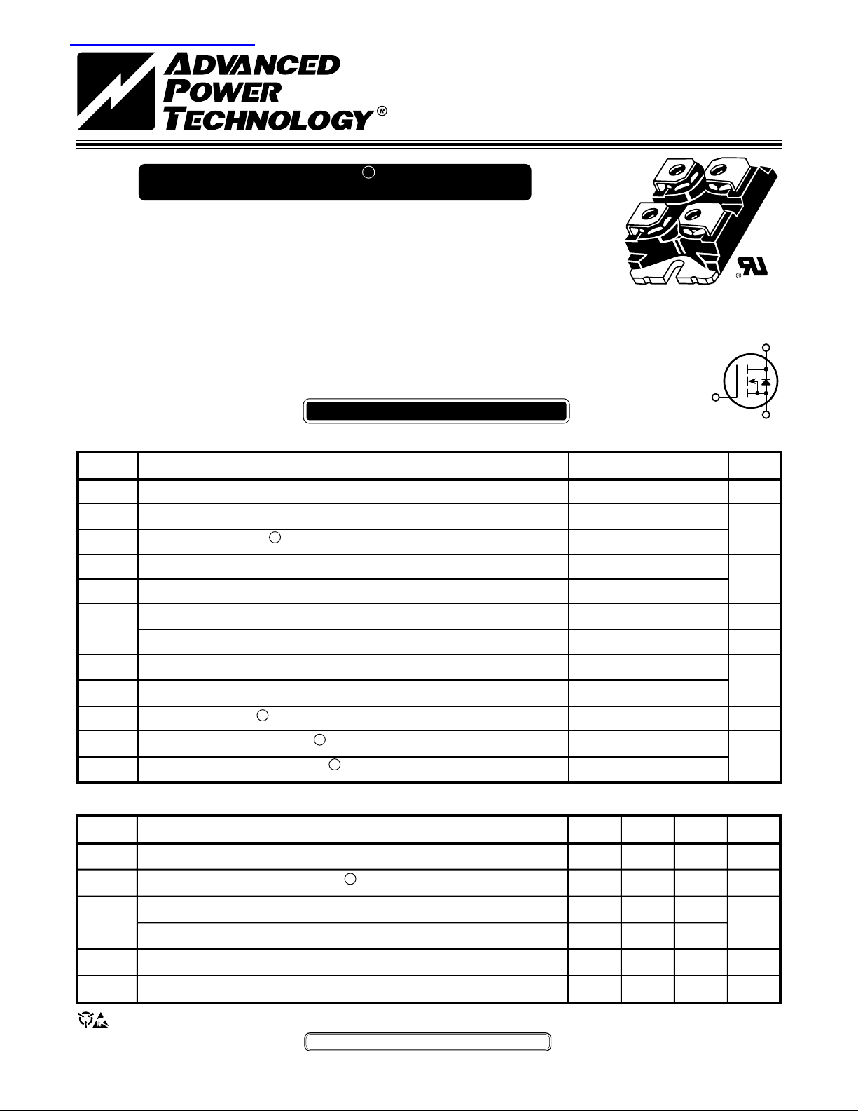
ISOTOP
S
D
"UL Recognized"
®
ΩΩ
Ω
ΩΩ
S
SOT-227
patented metal gate structure.
• Lower Input Capacitance •Increased Power Dissipation
• Lower Miller Capacitance • Easier To Drive
• Lower Gate Charge, Qg •Popular SOT-227 Package
•
FAST RECOVERY BODY DIODE
MAXIMUM RATINGS All Ratings: TC = 25°C unless otherwise specified.
Symbol
V
DSS
I
I
DM
V
V
GSM
P
TJ,T
T
I
AR
E
E
Parameter
Drain-Source Voltage
Continuous Drain Current @ T
D
Pulsed Drain Current
Gate-Source Voltage Continuous
GS
Gate-Source Voltage Transient
Total Power Dissipation @ TC = 25°C
D
Linear Derating Factor
Operating and Storage Junction Temperature Range
STG
Lead Temperature: 0.063" from Case for 10 Sec.
L
Avalanche Current
Repetitive Avalanche Energy
AR
Single Pulse Avalanche Energy
AS
1
1
(Repetitive and Non-Repetitive)
= 25°C
C
1
4
APT12067JFLL
1200
17
68
±30
±40
463
3.70
-55 to 150
300
17
50
2500
G
UNIT
Volts
Amps
Volts
Watts
W/°C
°C
Amps
mJ
D
S
STATIC ELECTRICAL CHARACTERISTICS
Symbol
BV
R
DS(on)
I
DSS
I
GSS
V
GS(th)
Characteristic / Test Conditions
Drain-Source Breakdown Voltage (V
DSS
Drain-Source On-State Resistance
Zero Gate Voltage Drain Current (V
Zero Gate Voltage Drain Current (VDS = 960V, VGS = 0V, TC = 125°C)
Gate-Source Leakage Current (VGS = ±30V, V
Gate Threshold Voltage (VDS = VGS, ID = 2.5mA)
CAUTION: These Devices are Sensitive to Electrostatic Discharge. Proper Handling Procedures Should Be Followed.
APT Website - http://www.advancedpower.com
= 0V, ID = 250µA)
GS
2
(VGS = 10V, ID = 8.5A)
= 1200V, VGS = 0V)
DS
= 0V)
DS
MIN TYP MAX
1200
35
0.670
250
1000
±100
UNIT
Volts
Ohms
µA
nA
Volts
050-7089 Rev B 2-2004
DYNAMIC CHARACTERISTICS
Note:
Duty Factor D =
t
1
/
t
2
Peak TJ = PDM x Z
θJC
+ T
C
t
1
t
2
P
DM
Symbol
C
C
oss
C
Q
Q
Q
t
d(on)
t
t
d(off)
t
E
E
E
E
Characteristic
Input Capacitance
iss
Output Capacitance
Reverse Transfer Capacitance
rss
Total Gate Charge
g
Gate-Source Charge
gs
Gate-Drain ("Miller ") Charge
gd
Turn-on Delay Time
Rise Time
r
Turn-off Delay Time
Fall Time
f
Turn-on Switching Energy
on
Turn-off Switching Energy
off
Turn-on Switching Energy
on
Turn-off Switching Energy
off
Test Conditions
V
= 0V
GS
= 25V
V
DS
f = 1 MHz
3
6
6
INDUCTIVE SWITCHING @ 25°C
INDUCTIVE SWITCHING @ 125°C
V
= 10V
GS
= 600V
V
DD
= 18A @ 25°C
I
D
RESISTIVE SWITCHING
= 15V
V
GS
= 600V
V
DD
= 18A @ 25°C
I
D
= 0.6Ω
R
G
V
= 800V, V
DD
= 18A, RG = 5Ω
I
D
V
= 800V, V
DD
= 18A, RG = 5Ω
I
D
GS
GS
= 15V
= 15V
SOURCE-DRAIN DIODE RATINGS AND CHARACTERISTICS
Symbol
I
I
SM
V
dv
t
Q
I
RRM
Characteristic / Test Conditions
Continuous Source Current (Body Diode)
S
1
Pulsed Source Current
Diode Forward Voltage
SD
/
Peak Diode Recovery dv/
dt
(Body Diode)
2
dt
Reverse Recovery Time
rr
= -ID 18A, di/dt = 100A/µs)
(I
S
Reverse Recovery Charge
rr
(IS = -ID 18A, di/dt = 100A/µs)
Peak Recovery Current
(IS = -ID 18A, di/dt = 100A/µs)
(VGS = 0V, IS = -ID 18A)
5
T
= 25°C 300
j
T
= 125°C 600
j
T
= 25°C 2.0
j
T
= 125°C 6.0
j
T
= 25°C 13
j
T
= 125°C 21
j
THERMAL CHARACTERISTICS
Symbol
R
R
1 Repetitive Rating: Pulse width limited by maximum junction
temperature
2 Pulse Test: Pulse width < 380 µs, Duty Cycle < 2%
3 See MIL-STD-750 Method 3471
APT Reserves the right to change, without notice, the specifications and information contained herein.
Characteristic
Junction to Case
θJC
Junction to Ambient
θJA
0.30
4 Starting T
dv
5
/
dt
device itself. I
6 Eon includes diode reverse recovery. See figures 18, 20.
+25°C, L = 17.30mH, R
j
=
numbers reflect the limitations of the test circuit rather than the
≤ -I
S
17A
D
MIN TYP MAX
4420
660
115
150
20
95
22
19
22
19
705
302
1239
402
MIN TYP MAX
MIN TYP MAX
25Ω, Peak IL = 17A
G
=
di
/
≤ 700A/µs V
dt
R
APT12067JFLL
17
68
1.3
18
0.27
40
≤ 1200 T
≤ 150°C
J
UNIT
pF
nC
ns
J
µ
UNIT
Amps
Volts
V/ns
ns
µC
Amps
UNIT
°C/W
050-7089 Rev B 2-2004
0.25
0.20
0.15
0.10
, THERMAL IMPEDANCE (°C/W)
JC
θ
0.05
Z
0
0.9
0.7
0.5
0.3
0.1
0.05
-5
10
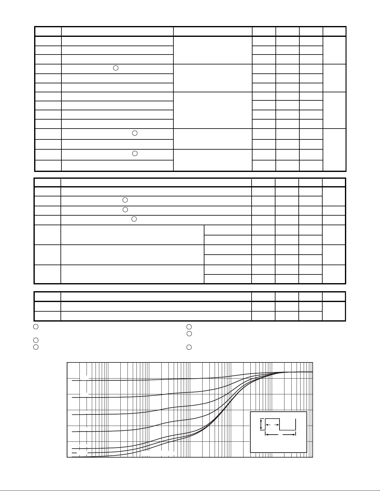
FIGURE 1, MAXIMUM EFFECTIVE TRANSIENT THERMAL IMPEDANCE, JUNCTION-TO-CASE vs PULSE DURATION
-4
10
SINGLE PULSE
-3
10
RECTANGULAR PULSE DURATION (SECONDS)
-2
10
-1
10
1.0 10

Typical Performance Curves
Junction
temp. (°C)
RC MODEL
0.0497
0.0256F
40
V
=15,10 & 8V
35
GS
APT12067JFLL
7V
6.5V
30
25
6V
Power
(watts)
Case temperature. (°C)
0.180
0.0393
0.419F
12.8F
20
15
10
, DRAIN CURRENT (AMPERES)
D
5
0
0 5 10 15 20 25 30
VDS, DRAIN-TO-SOURCE VOLTAGE (VOLTS)
FIGURE 2, TRANSIENT THERMAL IMPEDANCE MODEL FIGURE 3, LOW VOLTAGE OUTPUT CHARACTERISTICS
50
VDS> ID (ON) x R
250µSEC. PULSE TEST
45
@ <0.5 % DUTY CYCLE
DS(ON)
40
35
30
25
20
15
10
, DRAIN CURRENT (AMPERES)
D
MAX.
TJ = +125°C
TJ = +25°C
TJ = -55°C
1.40
NORMALIZED TO
V
= 10V @ ID = 8.5A
GS
1.30
1.20
VGS=10V
1.10
1.00
, DRAIN-TO-SOURCE ON RESISTANCE I
0.90
VGS=20V
05
0
0 1 2 3 4 5 6 7 0 5 10152025303540
VGS, GATE-TO-SOURCE VOLTAGE (VOLTS) ID, DRAIN CURRENT (AMPERES)
FIGURE 4, TRANSFER CHARACTERISTICS FIGURE 5, R
18
DS(ON)
0.80
1.15
vs DRAIN CURRENT
DS(ON)
16
14
12
10
8
6
4
, DRAIN CURRENT (AMPERES) I
D
2
0
25 50 7 5 100 125 150 -50 -25 0 25 50 75 100 125 150
FIGURE 6, MAXIMUM DRAIN CURRENT vs CASE TEMPERATURE FIGURE 7, BREAKDOWN VOLTAGE vs TEMPERATURE
, CASE TEMPERATURE (°C) TJ, JUNCTION TEMPERATURE (°C)
T
C
2.5
ID = 8.5A
VGS = 10V
2.0
1.10
1.05
1.00
0.95
, DRAIN-TO-SOURCE BREAKDOWN R
0.90
DSS
0.85
1.2
1.1
5.5V
5V
4.5V
1.5
1.0
0.9
1.0
(NORMALIZED)
0.5
, DRAIN-TO-SOURCE ON RESISTANCE I
DS(ON)
0.0
R
-50 -25 0 25 50 75 100 125 150 -50 -25 0 25 50 75 100 125 150
T
, JUNCTION TEMPERATURE (°C) TC, CASE TEMPERATURE (°C)
J
FIGURE 8, R
vs. TEMPERATURE FIGURE 9, THRESHOLD VOLTAGE vs TEMPERATURE
DS(ON)
(NORMALIZED) VOLTAGE (NORMALIZED)
0.8
, THRESHOLD VOLTAGE BV
GS(TH)
0.7
V
0.6
050-7089 Rev B 2-2004

68
OPERATION HERE
LIMITED BY R
20,000
(ON)
DS
100µS
10,000
5,000
APT12067JFLL
C
iss
10
500
C
oss
5
1,000
C
rss
, DRAIN CURRENT (AMPERES)
D
TC =+25°C
TJ =+150°C
SINGLE PULSE
1
1 10 100 1200 0 10 20 30 40 50
VDS, DRAIN-TO-SOURCE VOLTAGE (VOLTS) VDS, DRAIN-TO-SOURCE VOLTAGE (VOLTS)
1mS
10mS
100
10
FIGURE 10, MAXIMUM SAFE OPERATING AREA FIGURE 11,CAPACITANCE vs DRAIN-TO-SOURCE VOLTAGE
16
ID = 18A
200
100
12
T
=+150°C
VDS=240V
8
VDS=600V
VDS=960V
10
J
T
=+25°C
J
4
, GATE-TO-SOURCE VOLTAGE (VOLTS) I
GS
V
0
0 20 40 60 80 100 120 140 160 180200 0.3 0.5 0.7 0.9 1.1 1.3 1.5
Q
, TOTAL GATE CHARGE (nC) VSD, SOURCE-TO-DRAIN VOLTAGE (VOLTS)
g
, REVERSE DRAIN CURRENT (AMPERES) C, CAPACITANCE (pF)
DR
I
1
FIGURE 12, GATE CHARGE vs GATE-TO-SOURCE VOLTAGE FIGURE 13, SOURCE-DRAIN DIODE FORWARD VOLTAGE
(ns)
d(off)
and t
d(on)
160
140
t
d(off)
120
VDD = 800V
100
RG = 5Ω
TJ = 125°C
80
L = 100µH
60
40
20
0
0 10 20 30 0 5 1015202530
t
d(on)
ID (A) ID (A)
(ns)
f
and t
r
60
50
40
30
20
10
0
VDD = 800V
RG = 5Ω
TJ = 125°C
L = 100µH
t
f
t
r
FIGURE 14, DELAY TIMES vs CURRENT FIGURE 15, RISE AND FALL TIMES vs CURRENT
(µJ) t
off
and E
on
E
2000
VDD = 800V
RG = 5Ω
TJ = 125°C
L = 100µH
1500
EON includes
diode reverse recovery
1000
500
E
on
E
off
3000
VDD = 800V
ID = 18A
2500
TJ = 125°C
L = 100µH
EON includes
2000
diode reverse recovery
1500
E
on
1000
SWITCHING ENERGY (µJ) t
500
E
off
0
0 5 10 15 20 25 30 0 5 10 15 20 25 30 35 40 45 50
FIGURE 16, SWITCHING ENERGY vs CURRENT FIGURE 17, SWITCHING ENERGY VS. GATE RESISTANCE
050-7089 Rev B 2-2004
0
I
(A) RG, GATE RESISTANCE (Ohms)
D

APT12067JFLL
t
10%
d(on)
t
r
90%
5%
10%
Gate Voltage
Drain Current
5%
Drain Voltage
Switching Energy
Figure 18, Turn-on Switching Waveforms and Definitions
APT60D120B
V
V
CC
I
CE
C
G
TJ125°C
90%
t
d(off)
90%
t
f
Gate Voltage
Drain Voltage
TJ125°C
10%
Drain Current
0
Switching Energy
Figure 19, Turn-off Switching Waveforms and Definitions
D.U.T.
Figure 20, Inductive Switching Test Circuit
r = 4.0 (.157)
(2 places)
SOT-227 (ISOTOP®) Package Outline
11.8 (.463)
31.5 (1.240)
31.7 (1.248)
7.8 (.307)
8.2 (.322)
W=4.1 (.161)
W=4.3 (.169)
H=4.8 (.187)
H=4.9 (.193)
(4 places)
4.0 (.157)
4.2 (.165)
(2 places)
12.2 (.480)
8.9 (.350)
9.6 (.378)
0.75 (.030)
0.85 (.033)
Hex Nut M4
(4 places)
12.6 (.496)
12.8 (.504)
25.2 (0.992)
25.4 (1.000)
®
ISOTOP
is a Registered Trademark of SGS Thomson.
3.3 (.129)
14.9 (.587)
15.1 (.594)
30.1 (1.185)
30.3 (1.193)
38.0 (1.496)
38.2 (1.504)
3.6 (.143)
* Source Drain
* Source
Dimensions in Millimeters and (Inches)
APT’s products are covered by one or more of U.S.patents 4,895,810 5,045,903 5,089,434 5,182,234 5,019,522
1.95 (.077)
2.14 (.084)
*
Source terminals are shorted
internally. Current handling
capability is equal for either
Source terminal.
Gate
5,262,336 6,503,786 5,256,583 4,748,103 5,283,202 5,231,474 5,434,095 5,528,058 and foreign patents. US and Foreign patents pending. All Rights Reserved.
050-7089 Rev B 2-2004
 Loading...