

查询APT12040JVR供应商
APT12040JVR
1200V 26A 0.400W
POWER MOS V
®
Power MOS V® is a new generation of high voltage N-Channel enhancement
mode power MOSFETs. This new technology minimizes the JFET effect,
increases packing density and reduces the on-resistance. Power MOS V
also achieves faster switching speeds through optimized gate layout.
Faster Switching 100% Avalanche Tested
Lower Leakage Popular SOT-227 Package
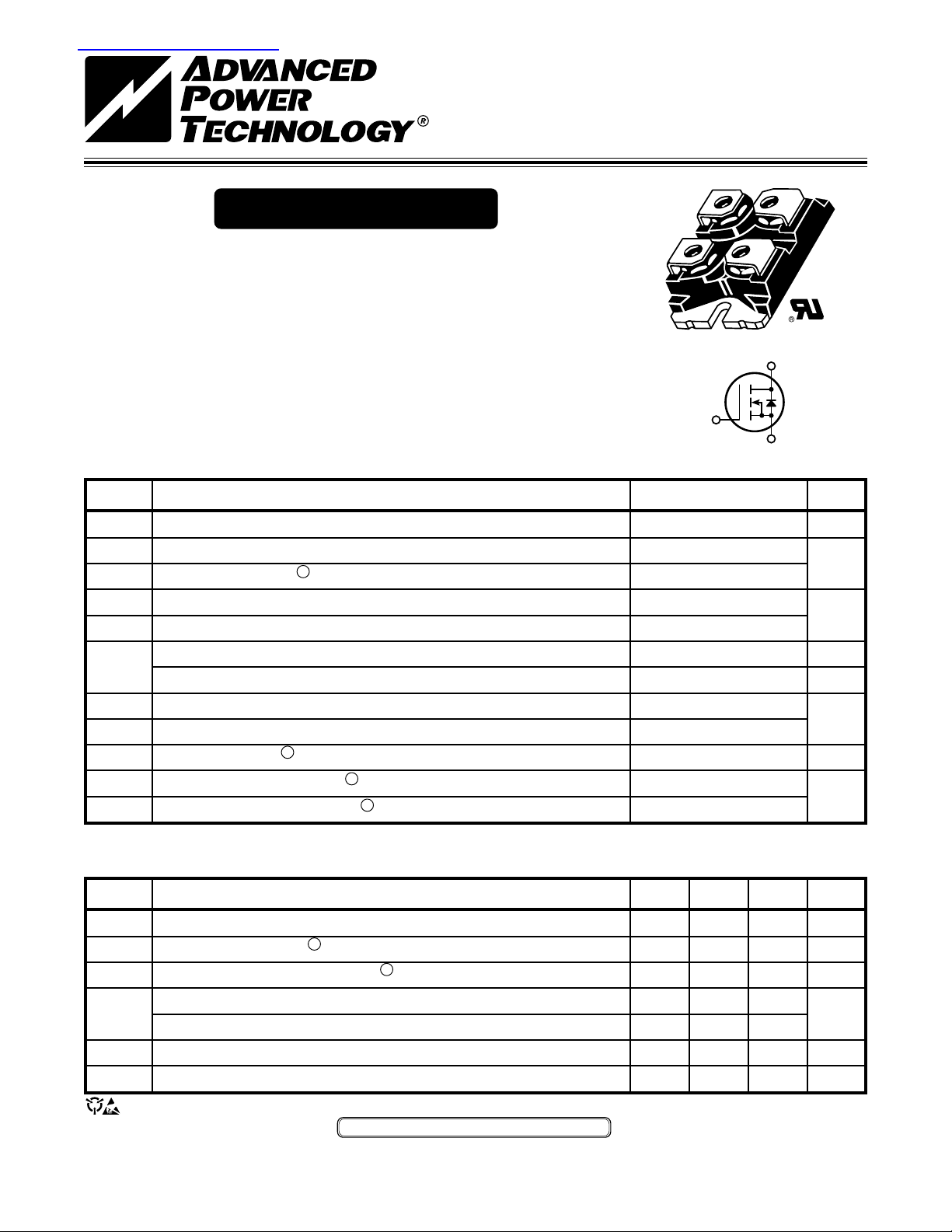
S
G
®
ISOTOP
G
D
®
S
SOT-227
"UL Recognized"
D
S
MAXIMUM RATINGS All Ratings: TC = 25°C unless otherwise specified.
Symbol
V
DSS
I
D
I
DM
V
GS
V
GSM
P
D
TJ,T
STG
T
L
I
AR
E
AR
E
AS
Parameter
Drain-Source Voltage
Continuous Drain Current @ T
Pulsed Drain Current
Gate-Source Voltage Continuous
Gate-Source Voltage Transient
Total Power Dissipation @ TC = 25°C
Linear Derating Factor
Operating and Storage Junction Temperature Range
Lead Temperature: 0.063" from Case for 10 Sec.
Avalanche Current
Repetitive Avalanche Energy
Single Pulse Avalanche Energy
1
1
(Repetitive and Non-Repetitive)
= 25°C
C
1
4
APT12040JVR
1200
26
104
±30
±40
700
5.6
-55 to 150
300
26
50
3600
UNIT
Volts
Amps
Volts
Watts
W/°C
°C
Amps
mJ
STATIC ELECTRICAL CHARACTERISTICS
Symbol
BV
I
D(on)
R
DS(on)
I
DSS
I
GSS
V
GS(th)
USA
405 S.W. Columbia Street Bend, Oregon 97702-1035 Phone: (541) 382-8028 FAX: (541) 388-0364
EUROPE
Chemin de Magret 33700 Merignac - France Phone: (33) 5 57 92 15 15 FAX: (33) 5 56 47 97 61
Characteristic / Test Conditions
Drain-Source Breakdown Voltage (V
DSS
On State Drain Current
Drain-Source On-State Resistance
Zero Gate Voltage Drain Current (VDS = V
Zero Gate Voltage Drain Current (V
Gate-Source Leakage Current (VGS = ±30V, V
Gate Threshold Voltage (VDS = VGS, ID = 5mA)
CAUTION: These Devices are Sensitive to Electrostatic Discharge. Proper Handling Procedures Should Be Followed.
2
(V
DS
APT Website - http://www.advancedpower.com
= 0V, ID = 250µA)
GS
> I
x R
D(on)
2
(VGS = 10V, 0.5 I
= 0.8 V
DS
Max, VGS = 10V)
DS(on)
D[Cont.]
, VGS = 0V)
DSS
, VGS = 0V, TC = 125°C)
DSS
= 0V)
DS
)
MIN TYP MAX
1200
26
24
0.400
100
500
±100
UNIT
Volts
Amps
Ohms
µA
nA
Volts
050-5588 Rev C
DYNAMIC CHARACTERISTICS APT12040JVR
Note:
Duty Factor D =
t
1
/
t
2
Peak TJ = PDM x Z
θJC
+ T
C
t
1
t
2
P
DM
Symbol
C
C
C
Q
Q
Q
t
d(on)
t
d(off)
Characteristic
Input Capacitance
iss
Output Capacitance
oss
Reverse Transfer Capacitance
rss
Total Gate Charge
g
Gate-Source Charge
gs
Gate-Drain ("Miller ") Charge
gd
Turn-on Delay Time
t
Rise Time
r
Turn-off Delay Time
t
Fall Time
f
Test Conditions
V
VDS = 25V
f = 1 MHz
3
V
GS
VDD = 0.5 V
ID = I
D[Cont.]
V
GS
V
= 0.5 V
DD
ID = I
D[Cont.]
R
G
SOURCE-DRAIN DIODE RATINGS AND CHARACTERISTICS
Symbol
I
I
SM
V
t
Q
Characteristic / Test Conditions
Continuous Source Current (Body Diode)
S
1
Pulsed Source Current
Diode Forward Voltage 2 (VGS = 0V, IS = -I
SD
Reverse Recovery Time (IS = -I
rr
Reverse Recovery Charge (I
rr
(Body Diode)
S
= -I
, dlS/dt = 100A/µs)
D[Cont.]
, dlS/dt = 100A/µs)
D[Cont.]
D[Cont.]
)
= 0V
GS
= 10V
@ 25°C
= 15V
@ 25°C
= 0.6W
DSS
DSS
MIN TYP MAX
15000 18000
1240 1730
640 960
800 1200
64 96
400 600
20 40
18 36
90 135
20 40
MIN TYP MAX
26
104
1.3
1400
38
UNIT
pF
nC
ns
UNIT
Amps
Volts
ns
µC
050-5588 Rev C
THERMAL/ PACKAGE CHARACTERISTICS
Symbol
R
R
V
Isolation
Torque
1
Repetitive Rating: Pulse width limited by maximum junction
temperature.
, Peak IL = 26A
2
Pulse Test: Pulse width < 380 µS, Duty Cycle < 2%
APT Reserves the right to change, without notice, the specifications and information contained herein.
Characteristic
Junction to Case
qJC
Junction to Ambient
qJA
RMS Voltage
(50-60 Hz Sinusoidal Waveform From Terminals to Mounting Base for 1 Min.)
Maximum Torque for Device Mounting Screws and Electrical Terminations.
3
See MIL-STD-750 Method 3471
4
Starting T
0.2
0.1
0.05
0.01
0.005
, THERMAL IMPEDANCE (°C/W)
JC
q
Z
0.001
0.0005
10
D=0.5
0.2
0.1
0.05
0.02
0.01
SINGLE PULSE
-5
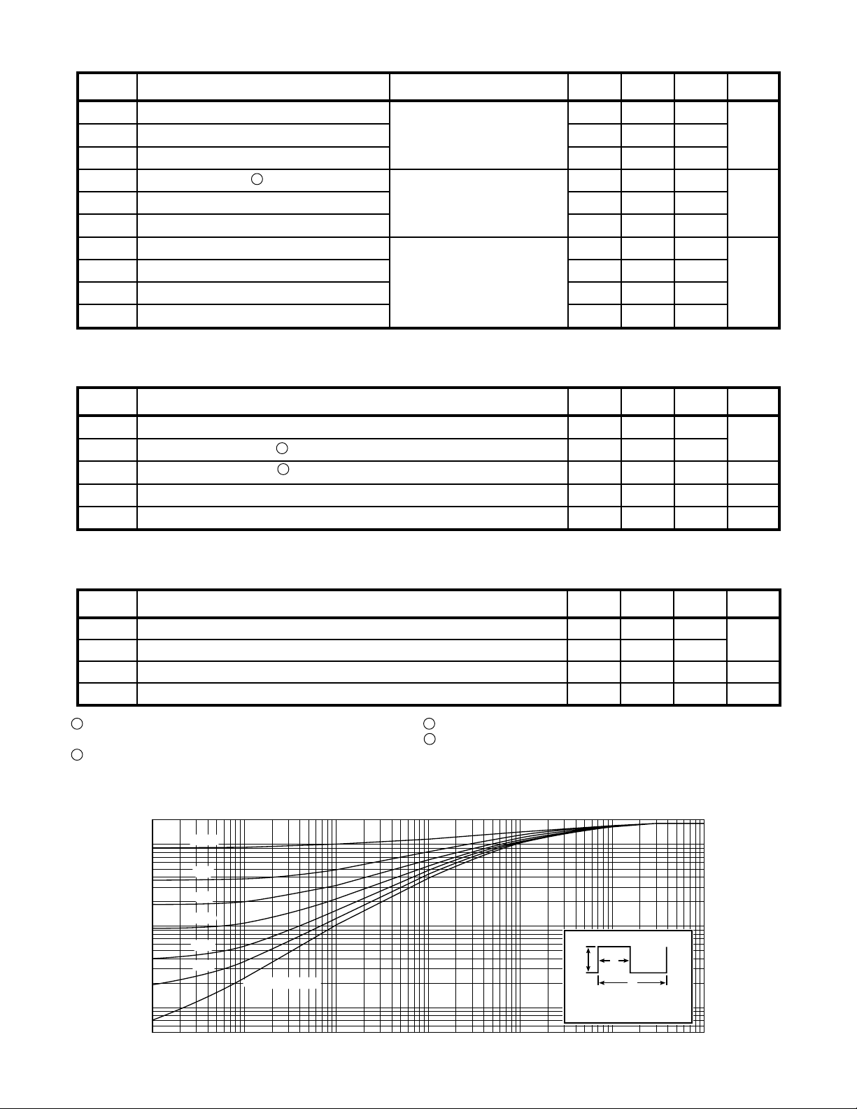
FIGURE 1, MAXIMUM EFFECTIVE TRANSIENT THERMAL IMPEDANCE, JUNCTION-TO-CASE vs PULSE DURATION
-4
10
-3
10
RECTANGULAR PULSE DURATION (SECONDS)
-2
10
+25°C, L = 10.65mH, R
j
=
10
MIN TYP MAX
0.18
40
2500
13
25W
G
=
-1
1.0 10
UNIT
°C/W
Volts
lbin

APT12040JVR
50
VGS=6V, 7V, 10V & 15V
40
5V
50
40
VGS=6V, 7V, 10V & 15V
5V
30
20
30
20
4.5V
10
, DRAIN CURRENT (AMPERES)
D
0
0 100 200 300 400 500 600 0 4 8 12 16 20
VDS, DRAIN-TO-SOURCE VOLTAGE (VOLTS) VDS, DRAIN-TO-SOURCE VOLTAGE (VOLTS)
4V
10
, DRAIN CURRENT (AMPERES)
D
0
FIGURE 2, TYPICAL OUTPUT CHARACTERISTICS FIGURE 3, TYPICAL OUTPUT CHARACTERISTICS
50
VDS> ID (ON) x RDS (ON)MAX.
250µSEC. PULSE TEST
@ <0.5 % DUTY CYCLE
40
30
20
TJ = +125°C
10
, DRAIN CURRENT (AMPERES) I
D
0
FIGURE 4, TYPICAL TRANSFER CHARACTERISTICS FIGURE 5, RDS(ON) vs DRAIN CURRENT
TJ = +25°C
02468 01530456075
V
, GATE-TO-SOURCE VOLTAGE (VOLTS) ID, DRAIN CURRENT (AMPERES)
GS
TJ = -55°C
30
1.20
NORMALIZED TO
V
= 10V @ 0.5 ID [Cont.]
GS
1.15
1.10
1.05
VGS=10V
VGS=20V
1.00
(ON), DRAIN-TO-SOURCE ON RESISTANCE I
0.95
DS
1.15
4.5V
4V
, DRAIN-TO-SOURCE BREAKDOWN R
1.10
1.05
1.00
0.95
0.90
DSS
0.85
1.2
1.1
25
20
15
10
, DRAIN CURRENT (AMPERES) I
5
D
0
25 50 75 100 125 150 -50 -25 0 25 50 75 100 125 150
FIGURE 6, MAXIMUM DRAIN CURRENT vs CASE TEMPERATURE FIGURE 7, BREAKDOWN VOLTAGE vs TEMPERATURE
2.5
, CASE TEMPERATURE (°C) TJ, JUNCTION TEMPERATURE (°C)
T
C
ID = 0.5 ID [Cont.]
VGS = 10V
2.0
1.0
1.5
0.9
1.0
(NORMALIZED)
0.5
(ON), DRAIN-TO-SOURCE ON RESISTANCE I
0.0
DS
-50 -25 0 25 50 75 100 125 150 -50 -25 0 25 50 75 100 125 150
R
T
, JUNCTION TEMPERATURE (°C) TC, CASE TEMPERATURE (°C)
J
FIGURE 8, ON-RESISTANCE vs. TEMPERATURE FIGURE 9, THRESHOLD VOLTAGE vs TEMPERATURE
0.8
(NORMALIZED) VOLTAGE (NORMALIZED)
(TH), THRESHOLD VOLTAGE BV
0.7
GS
V
0.6
050-5588 Rev C

200
100
50
OPERATION HERE
LIMITED BY R
10
5
1
TC =+25°C
.5
, DRAIN CURRENT (AMPERES)
D
TJ =+150°C
SINGLE PULSE
.1
1 5 10 50 100 500 1200 .01 .1 1 10 50
VDS, DRAIN-TO-SOURCE VOLTAGE (VOLTS) VDS, DRAIN-TO-SOURCE VOLTAGE (VOLTS)
FIGURE 10, MAXIMUM SAFE OPERATING AREA FIGURE 11, TYPICAL CAPACITANCE vs DRAIN-TO-SOURCE VOLTAGE
20
ID = ID [Cont.]
16
12
(ON)
DS
VDS=120V
VDS=240V
10µS
100µS
1mS
10mS
100mS
70,000
50,000
10,000
5,000
1,000
400
200
100
C
iss
C
oss
C
rss
50
T
=+150°C T
J
=+25°C
J
APT12040JVR
8
4
, GATE-TO-SOURCE VOLTAGE (VOLTS) I
GS
V
0
0 250 500 750 1000 1250 1500 0.2 0.4 0.6 0.8 1.0 1.2 1.4
Q
, TOTAL GATE CHARGE (nC) VSD, SOURCE-TO-DRAIN VOLTAGE (VOLTS)
FIGURE 12, GATE CHARGES vs GATE-TO-SOURCE VOLTAGE FIGURE 13, TYPICAL SOURCE-DRAIN DIODE FORWARD VOLTAGE
g
VDS=600V
10
5
, REVERSE DRAIN CURRENT (AMPERES) C, CAPACITANCE (pF)
DR
1
I
SOT-227 (ISOTOP®) Package Outline
11.8 (.463)
12.2 (.480)
8.9 (.350)
9.6 (.378)
Hex Nut M4
(4 places)
0.75 (.030)
0.85 (.033)
12.6 (.496)
12.8 (.504)
25.2 (0.992)
25.4 (1.000)
r = 4.0 (.157)
(2 places)
31.5 (1.240)
31.7 (1.248)
7.8 (.307)
8.2 (.322)
W=4.1 (.161)
W=4.3 (.169)
H=4.8 (.187)
H=4.9 (.193)
(4 places)
4.0 (.157)
4.2 (.165)
(2 places)
14.9 (.587)
15.1 (.594)
3.3 (.129)
3.6 (.143)
* Source Drain
1.95 (.077)
2.14 (.084)
30.1 (1.185)
30.3 (1.193)
38.0 (1.496)
38.2 (1.504)
* Source
Gate
Dimensions in Millimeters and (Inches)
®
ISOTOP
is a Registered Trademark of SGS Thomson.
APT's devices are covered by one or more of the following U.S.patents: 4,895,810 5,045,903 5,089,434 5,182,234 5,019,522 5,262,336
050-5588 Rev C
5,256,583 4,748,103 5,283,202 5,231,474 5,434,095 5,528,058
*
Source terminals are shorted
internally. Current handling
capability is equal for either
Source terminal.
"UL Recognized" File No. E145592
 Loading...