

查询APT10M07供应商
APT10M07JVR
100V 225A 0.007Ω
POWER MOS V
®
Power MOS V® is a new generation of high voltage N-Channel enhancement
mode power MOSFETs. This new technology minimizes the JFET effect,
increases packing density and reduces the on-resistance. Power MOS V
also achieves faster switching speeds through optimized gate layout.
• Faster Switching • 100% Avalanche Tested
• Lower Leakage • Popular SOT-227 Package
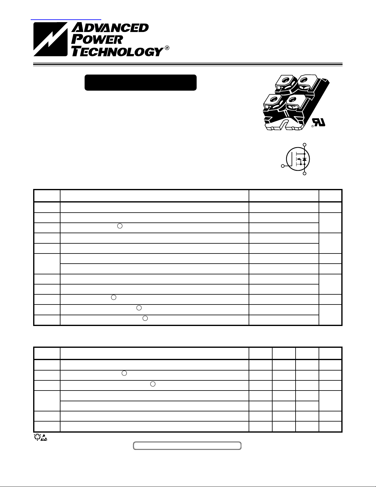
S
G
®
ISOTOP
G
D
®
S
SOT-227
"UL Recognized"
D
S
MAXIMUM RATINGS All Ratings: TC = 25°C unless otherwise specified.
Symbol
V
DSS
I
D
I
DM
V
GS
V
GSM
P
D
TJ,T
STG
T
L
I
AR
E
AR
E
AS
Parameter
Drain-Source Voltage
Continuous Drain Current @ T
Pulsed Drain Current
Gate-Source Voltage Continuous
Gate-Source Voltage Transient
Total Power Dissipation @ T
Linear Derating Factor
Operating and Storage Junction Temperature Range
Lead Temperature: 0.063" from Case for 10 Sec.
Avalanche Current
Repetitive Avalanche Energy
Single Pulse Avalanche Energy
1
1
(Repetitive and Non-Repetitive)
= 25°C
C
= 25°C
C
1
4
APT10M07JVR
100
225
900
±30
±40
700
5.6
-55 to 150
300
225
50
3600
UNIT
Volts
Amps
Volts
Watts
W/°C
°C
Amps
mJ
STATIC ELECTRICAL CHARACTERISTICS
Symbol
BV
I
D(on)
R
DS(on)
I
DSS
I
GSS
V
GS(th)
USA
405 S.W. Columbia Street Bend, Oregon 97702-1035 Phone: (541) 382-8028 FAX: (541) 388-0364
EUROPE
Avenue J.F. Kennedy Bât B4 Parc Cadéra Nord F-33700 Merignac - France Phone: (33) 5 5792 1515 FAX: (33) 556 4797 61
Characteristic / Test Conditions
Drain-Source Breakdown Voltage (V
DSS
On State Drain Current
Drain-Source On-State Resistance
Zero Gate Voltage Drain Current (VDS = V
Zero Gate Voltage Drain Current (V
Gate-Source Leakage Current (VGS = ±30V, V
Gate Threshold Voltage (VDS = VGS, ID = 5.0mA)
CAUTION: These Devices are Sensitive to Electrostatic Discharge. Proper Handling Procedures Should Be Followed.
2
(V
DS
APT Website - http://www.advancedpower.com
= 0V, ID = 250µA)
GS
> I
x R
D(on)
2
(VGS = 10V, 0.5 I
= 0.8 V
DS
Max, VGS = 10V)
DS(on)
D[Cont.]
, VGS = 0V)
DSS
, VGS = 0V, TC = 125°C)
DSS
= 0V)
DS
)
MIN TYP MAX
100
225
24
0.007
250
1000
±100
UNIT
Volts
Amps
Ohms
µA
nA
Volts
050-5584 Rev B
DYNAMIC CHARACTERISTICS
Note:
Duty Factor D =
t
1
/
t
2
Peak TJ = PDM x Z
θJC
+ T
C
t
1
t
2
P
DM
APT10M07JVR
Symbol
C
iss
C
oss
C
rss
Q
g
Q
gs
Q
gd
t
d(on)
t
r
t
d(off)
t
f
Characteristic
Input Capacitance
Output Capacitance
Reverse Transfer Capacitance
Total Gate Charge
3
Gate-Source Charge
Gate-Drain ("Miller") Charge
Turn-on Delay Time
Rise Time
Turn-off Delay Time
Fall Time
Test Conditions
V
VDS = 25V
f = 1 MHz
V
GS
VDD = 0.5 V
ID = 100A @ 25°C
VGS = 15V
VDD = 0.5 V
ID = I
D[Cont.]
RG = 0.6Ω
SOURCE-DRAIN DIODE RATINGS AND CHARACTERISTICS
Symbol
I
I
SM
V
t
Q
Characteristic / Test Conditions
Continuous Source Current (Body Diode)
S
1
Pulsed Source Current
Diode Forward Voltage 2 (VGS = 0V, IS = -I
SD
Reverse Recovery Time (IS = -I
rr
Reverse Recovery Charge (I
rr
(Body Diode)
S
= -I
, dlS/dt = 100A/µs)
D[Cont.]
, dlS/dt = 100A/µs)
D[Cont.]
D[Cont.]
)
= 0V
GS
= 10V
DSS
DSS
@ 25°C
MIN TYP MAX
18000 21600
6800 9500
2800 4200
700 1050
130 195
300 435
25 50
60 120
80 120
20 40
MIN TYP MAX
225
900
1.3
330
3
UNIT
pF
nC
ns
UNIT
Amps
Volts
ns
µC
050-5584 Rev B
THERMAL/PACKAGE CHARACTERISTICS
Symbol
R
R
V
Isolation
Torque
1
Repetitive Rating: Pulse width limited by maximum junction
temperature.
2
Pulse Test: Pulse width < 380 µS, Duty Cycle < 2%
APT Reserves the right to change, without notice, the specifications and information contained herein.
Characteristic
Junction to Case
θJC
Junction to Ambient
θJA
RMS Voltage
(50-60 Hz Sinusoidal Waveform From Terminals to Mounting Base for 1 Min.)
Maximum Torque for Device Mounting Screws and Electrical Terminations.
3
See MIL-STD-750 Method 3471
4
Starting T
0.2
D=0.5
0.2
0.1
0.05
0.02
0.01
SINGLE PULSE
-5
FIGURE 1, MAXIMUM EFFECTIVE TRANSIENT THERMAL IMPEDANCE, JUNCTION-TO-CASE vs PULSE DURATION
-4
10
-3
10
RECTANGULAR PULSE DURATION (SECONDS)
-2
10
, THERMAL IMPEDANCE (°C/W)
Z
0.005
JC
θ
0.001
0.0005
0.1
0.05
0.01
10
+25°C, L = 142µH, R
j
=
-1
10
MIN TYP MAX
0.18
40
2500
13
25Ω, Peak IL = 225A
G
=
1.0 10
UNIT
°C/W
Volts
lb•in

APT10M07JVR
360
300
240
180
120
VGS=7V, 8V, 9V, 10V & 15V
6.5V
6V
5.5V
360
300
240
180
120
VGS=15V
10V
9V
8V
7V
6.5V
6V
5.5V
, DRAIN CURRENT (AMPERES)
60
D
5V
, DRAIN CURRENT (AMPERES)
60
D
4.5V
0
0 10 20 30 40 50 0 0.5 1.0 1.5 2.0 2.5
VDS, DRAIN-TO-SOURCE VOLTAGE (VOLTS) VDS, DRAIN-TO-SOURCE VOLTAGE (VOLTS)
0
FIGURE 2, TYPICAL OUTPUT CHARACTERISTICS FIGURE 3, TYPICAL OUTPUT CHARACTERISTICS
360
300
240
VDS> ID (ON) x RDS (ON)MAX.
250µSEC. PULSE TEST
@ <0.5 % DUTY CYCLE
180
TJ = -55°C
TJ = +25°C
TJ = +125°C
120
, DRAIN CURRENT (AMPERES) I
60
D
0
02468 0100200300400
V
GS
FIGURE 4, TYPICAL TRANSFER CHARACTERISTICS FIGURE 5, RDS(ON) vs DRAIN CURRENT
TJ = +125°C
TJ = +25°C
TJ = -55°C
, GATE-TO-SOURCE VOLTAGE (VOLTS) ID, DRAIN CURRENT (AMPERES)
250
200
1.10
1.05
NORMALIZED TO
V
= 10V @ 0.5 ID [Cont.]
GS
VGS=10V
1.00
0.95
0.90
0.85
(ON), DRAIN-TO-SOURCE ON RESISTANCE I
0.80
DS
VGS=20V
1.15
1.10
5V
4.5V
150
100
50
, DRAIN CURRENT (AMPERES) I
D
0
25 50 75 100 125 150 -50 -25 0 25 50 75 100 125 150
T
, CASE TEMPERATURE (°C) TJ, JUNCTION TEMPERATURE (°C)
FIGURE 6, MAXIMUM DRAIN CURRENT vs CASE TEMPERATURE FIGURE 7, BREAKDOWN VOLTAGE vs TEMPERATURE
2.00
C
ID = 0.5 ID [Cont.]
VGS = 10V
1.75
1.50
1.25
1.00
(NORMALIZED)
0.75
(ON), DRAIN-TO-SOURCE ON RESISTANCE I
0.50
DS
-50 -25 0 25 50 75 100 125 150 -50 -25 0 25 50 75 100 125 150
R
T
, JUNCTION TEMPERATURE (°C) TC, CASE TEMPERATURE (°C)
J
FIGURE 8, ON-RESISTANCE vs. TEMPERATURE FIGURE 9, THRESHOLD VOLTAGE vs TEMPERATURE
1.05
1.00
0.95
, DRAIN-TO-SOURCE BREAKDOWN R
DSS
0.90
1.2
1.1
1.0
0.9
0.8
(NORMALIZED) VOLTAGE (NORMALIZED)
(TH), THRESHOLD VOLTAGE BV
0.7
GS
V
0.6
050-5584 Rev B

1,000
OPERATION HERE
LIMITED BY RDS (ON)
500
100
50
10
TC =+25°C
5
, DRAIN CURRENT (AMPERES)
D
TJ =+150°C
SINGLE PULSE
10µS
100µS
1mS
10mS
100mS
DC
50,000
10,000
5,000
APT10M07JVR
C
iss
C
oss
C
rss
1
1 5 10 50 100 .01 .1 1 10 50
VDS, DRAIN-TO-SOURCE VOLTAGE (VOLTS) VDS, DRAIN-TO-SOURCE VOLTAGE (VOLTS)
FIGURE 10, MAXIMUM SAFE OPERATING AREA FIGURE 11, TYPICAL CAPACITANCE vs DRAIN-TO-SOURCE VOLTAGE
20
ID = 100A
16
12
8
4
, GATE-TO-SOURCE VOLTAGE (VOLTS) I
GS
V
0
0 200 400 600 800 1000 1200 1400 0 0.4 0.8 1.2 1.6 2.0
Q
, TOTAL GATE CHARGE (nC) VSD, SOURCE-TO-DRAIN VOLTAGE (VOLTS)
FIGURE 12, GATE CHARGES vs GATE-TO-SOURCE VOLTAGE FIGURE 13, TYPICAL SOURCE-DRAIN DIODE FORWARD VOLTAGE
g
VDS=20V
VDS=50V
VDS=80V
1,000
500
T
=+150°C T
100
50
10
, REVERSE DRAIN CURRENT (AMPERES) C, CAPACITANCE (pF)
DR
I
J
5
1
=+25°C
J
SOT-227 (ISOTOP®) Package Outline
11.8 (.463)
31.5 (1.240)
31.7 (1.248)
7.8 (.307)
8.2 (.322)
W=4.1 (.161)
W=4.3 (.169)
H=4.8 (.187)
H=4.9 (.193)
(4 places)
12.2 (.480)
8.9 (.350)
9.6 (.378)
Hex Nut M4
(4 places)
r = 4.0 (.157)
(2 places)
14.9 (.587)
15.1 (.594)
4.0 (.157)
4.2 (.165)
(2 places)
3.3 (.129)
3.6 (.143)
* Source Drain
0.75 (.030)
0.85 (.033)
1.95 (.077)
2.14 (.084)
30.1 (1.185)
30.3 (1.193)
38.0 (1.496)
38.2 (1.504)
* Source
Gate
Dimensions in Millimeters and (Inches)
®
ISOTOP
is a Registered Trademark of SGS Thomson.
APT's devices are covered by one or more of the following U.S.patents: 4,895,810 5,045,903 5,089,434 5,182,234 5,019,522 5,262,336
050-5584 Rev B
5,256,583 4,748,103 5,283,202 5,231,474 5,434,095 5,528,058
25.2 (0.992)
12.6 (.496)
25.4 (1.000)
12.8 (.504)
*
Source terminals are shorted
internally. Current handling
capability is equal for either
Source terminal.
"UL Recognized" File No. E145592
 Loading...