

查询APT100GF60JU3供应商
APT100GF60JU3
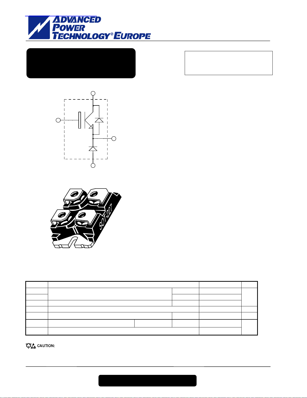
ISOTOP® Buck chopper
NPT IGBT
G
E
G
ISOTOP
C
A
A
C
Ò
Application
· AC and DC motor control
· Switched Mode Power Supplies
Features
E
· Non Punch Through (NPT) THUNDERBOLT IGBT®
- Low voltage drop
- Low tail current
- Switching frequency up to 100 kHz
- Soft recovery parallel diodes
- Low diode VF
- Low leakage current
- Avalanche energy rated
- RBSOA and SCSOA rated
· ISOTOP
· Very low stray inductance
· High level of integration
Benefits
· Outstanding performance at high frequency operation
· Stable temperature behavior
· Very rugged
· Direct mounting to heatsink (isolated package)
· Low junction to case thermal resistance
· Easy paralleling due to positive TC of VCEsat
V
I
®
Package (SOT-227)
Absolute maximum ratings
Symbol Parameter Max ratings Unit
Collector - Emitter Breakdown Voltage 600 V
V
CES
IC1
IC2
ICM Pulsed Collector Current TC = 25°C 320
VGE Gate – Emitter Voltage ±20 V
PD Maximum Power Dissipation TC = 25°C 416 W
IFAV Maximum Average Forward Current Duty cycle=0.5 TC = 80°C 30
IF
RMS
Continuous Collector Current
RMS Forward Current (Square wave, 50% duty) 39
T
= 25°C
C
TC = 80°C 100
These Devices are sensitive to Electrostatic Discharge. Proper Handing Procedures Should Be Followed.
= 600V
CES
= 100A @ Tc = 80°C
C
120
A
A
APT website –http://www.advancedpower.com
1-9
APT100GF60JU3– Rev 0 April, 2004

APT100GF60JU3
All ratings @ Tj = 25°C unless otherwise specified
Electrical Characteristics
Symbol Characteristic Test Conditions Min Typ Max Unit
BV
Collector - Emitter Breakdown Voltage VGE = 0V, IC = 100µA
CES
= 0V
V
I
Zero Gate Voltage Collector Current
CES
V
Collector Emitter on Voltage
CE(on)
V
Gate Threshold Voltage VGE = VCE, IC = 1mA 3 5 V
GE(th)
I
Gate – Emitter Leakage Current VGE = ±20V, VCE = 0V ±150 nA
GES
GE
= 600V
V
CE
=15V
V
GE
= 100A
I
C
Tj = 25°C
T
= 125°C
j
Tj = 25°C
T
= 125°C
j
Dynamic Characteristics
Symbol Characteristic Test Conditions Min Typ Max Unit
C
Input Capacitance 4300
ies
C
Output Capacitance 470
oes
C
Reverse Transfer Capacitance
res
Qg Total gate Charge 330
Qge Gate – Emitter Charge 290
Qgc Gate – Collector Charge
T
Turn-on Delay Time 26
d(on)
T
Rise Time 25
r
T
Turn-off Delay Time 150
d(off)
T
Fall Time 30
f
Eon Turn-on Switching Energy 3.35
E
Turn off Switching Energy
off
T
Turn-on Delay Time 26
d(on)
T
Rise Time 25
r
T
Turn-off Delay Time 170
d(off)
T
Fall Time 40
f
Eon Turn-on Switching Energy 4.3
E
Turn-off Switching Energy
off
= 0V
V
GE
V
= 25V
CE
f = 1MHz
V
= 15V
GS
= 300V
V
Bus
= 100A
I
C
Resistive Switching (25°C)
= 15V
V
GE
= 400V
V
Bus
= 100A
I
C
= 5W
R
G
Inductive Switching (125°C)
= 15V
V
GE
= 400V
V
Bus
= 100A
I
C
= 5W
R
G
600
V
100
1000
2.0 2.5
2.2
400
200
2.85
3.5
µA
V
pF
nC
ns
mJ
ns
mJ
APT website –http://www.advancedpower.com
2-9
APT100GF60JU3– Rev 0 April, 2004

APT100GF60JU3
Diode ratings and characteristics
Symbol Characteristic Test Conditions Min Typ Max Unit
= 30A 1.6 1.8
I
VF Diode Forward Voltage
IRM Maximum Reverse Leakage Current
F
IF = 60A 1.9
= 30A Tj = 125°C 1.4
I
F
VR = 600V Tj = 25°C 250
V
= 600V Tj = 125°C 500
R
CT Junction Capacitance VR = 200V 44 pF
=1A,VR=30V
I
Reverse Recovery Time
trr
Reverse Recovery Time
I
Maximum Reverse Recovery Current
RRM
Qrr Reverse Recovery Charge
trr Reverse Recovery Time 70 ns
Qrr Reverse Recovery Charge 1300 nC
I
Maximum Reverse Recovery Current
RRM
F
di/dt =100A/µs
I
= 30A
F
= 400V
V
R
di/dt =200A/µs
= 30A
I
F
= 400V
V
R
di/dt =1000A/µs
= 25°C 23
T
j
Tj = 25°C 85
= 125°C 160
T
j
Tj = 25°C 4
T
= 125°C 8
j
Tj = 25°C 130
= 125°C 700
T
j
Tj = 125°C
30 A
Thermal and package characteristics
Symbol Characteristic Min Typ Max Unit
R
Junction to Case
thJC
R
Junction to Ambient (IGBT & Diode) 20
thJA
V
TJ,T
RMS Isolation Voltage, any terminal to case t =1 min, I isol<1mA, 50/60Hz
ISOL
Storage Temperature Range -55 150
STG
TL Max Lead Temp for Soldering:0.063” from case for 10 sec 300
Torque Mounting torque (Mounting = 8-32 or 4mm Machine and terminals = 4mm Machine) 1.5 N.m
Wt Package Weight 29.2 g
IGBT 0.3
Diode 1.21
2500 V
V
µA
ns
A
nC
°C/W
°C
APT website –http://www.advancedpower.com
3-9
APT100GF60JU3– Rev 0 April, 2004
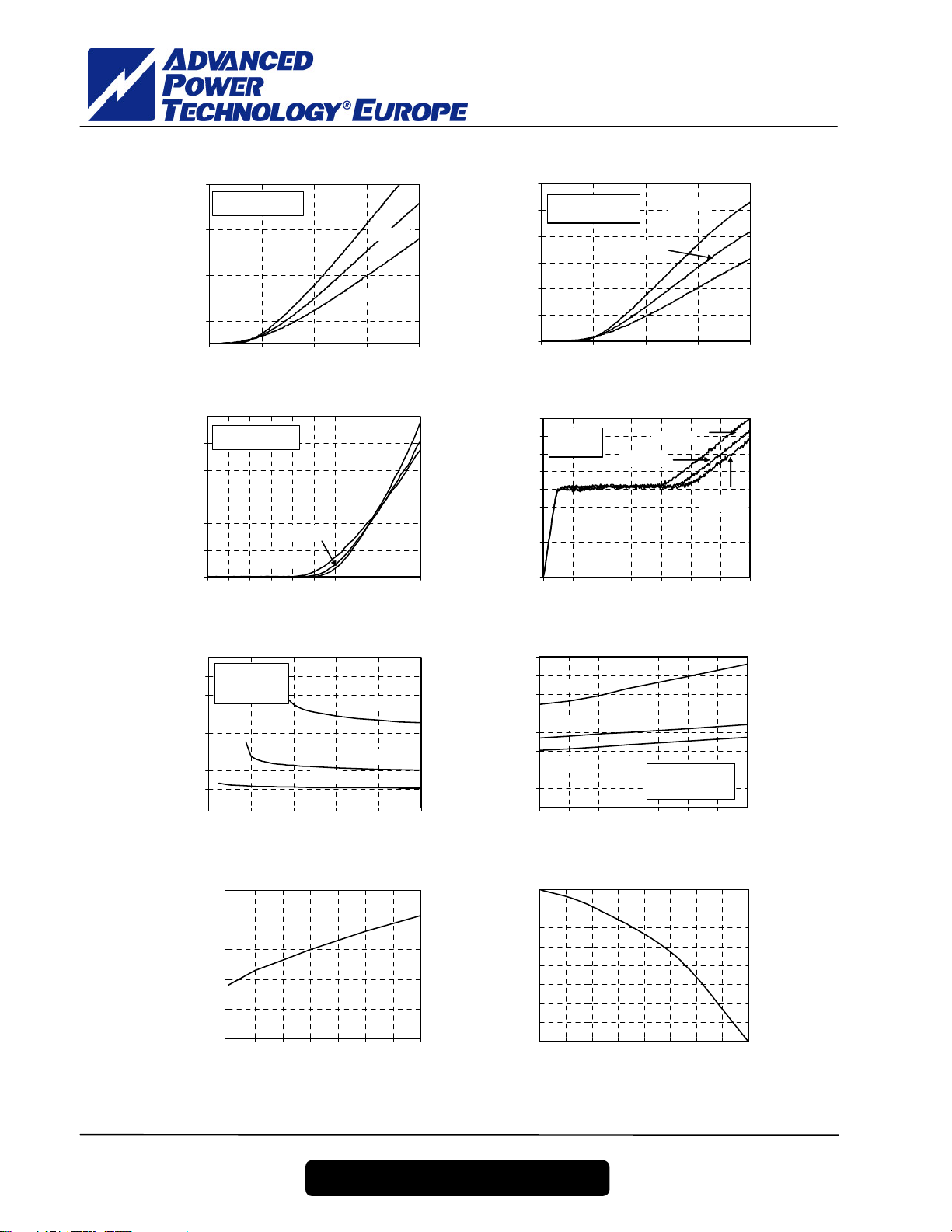
Typical IGBT Performance Curve
V
Output characteristics (VGE=15V)
350
250µs Pulse Test
300
< 0.5% Duty cycle
250
200
150
100
50
Ic, Collector Current (A)
0
01234
VCE, Collector to Emitter Voltage (V)
Tc=-55°C
Tc=25°C
Tc=12 5°C
APT100GF60JU3
Output Characteristics (VGE=10V)
300
250µs Pulse Test
250
< 0.5% Duty cycle
200
150
100
50
Ic, Collector Current (A)
0
01234
VCE, Collector to Emitter Voltage (V)
Tc=25°C
Tc=-55°C
Tc=125°C
300
250
200
150
100
50
Ic, Collector Current (A)
0
012345678910
On state Voltage vs Gate to Emitter Volt.
8
7
6
5
4
3
2
1
, Collector to Emitter Voltage (V)
CE
0
V
6 8 10 12 14 16
Transfer Characteristi cs
250µs Pulse Test
< 0.5% Duty cycle
TJ=25°C
TJ=125°C
VGE, Gate to Emitter Voltage (V)
TJ = 25°C
250µs Pulse T est
< 0.5% Duty cycle
Ic=50A
, Gate to Emitter Voltage (V)
V
GE
TJ=-55°C
Ic=200A
Ic=100A
18
IC = 100A
16
T
= 25°C
J
14
12
10
8
6
4
2
, Gate to Emitter Voltage (V)
GE
0
0 50 100 150 2 00 250 300 350
On state Voltage vs Junction Temperature
4
3.5
Ic=200A
3
2.5
Ic=100A
2
1.5
Ic=50A
1
, Collector to Emitter Voltage (V)
0.5
CE
V
0
-50 -25 0 25 50 75 100 125
T
Gate Charge
VCE=120V
VCE=300V
Gate Charge (nC)
250µs Pulse Test
< 0.5% Duty cycle
= 15V
V
GE
, Junction Temperature (°C)
J
VCE=480V
Breakdown Voltage vs Junction Temp.
1.20
1.10
1.00
0.90
Voltage (Norma lized)
0.80
Collector to Emitter Breakdown
0.70
-50 -25 0 25 50 75 100 125
T
, Junction Temperature (°C)
J
DC Collector Current vs Case Temperature
160
140
120
100
80
60
40
20
Ic, DC Collector Current (A)
0
-50 - 25 0 25 50 75 100 12 5 15 0
TC, Case Temperature (°C)
APT website –http://www.advancedpower.com
4-9
APT100GF60JU3– Rev 0 April, 2004
APT100GF60JU3
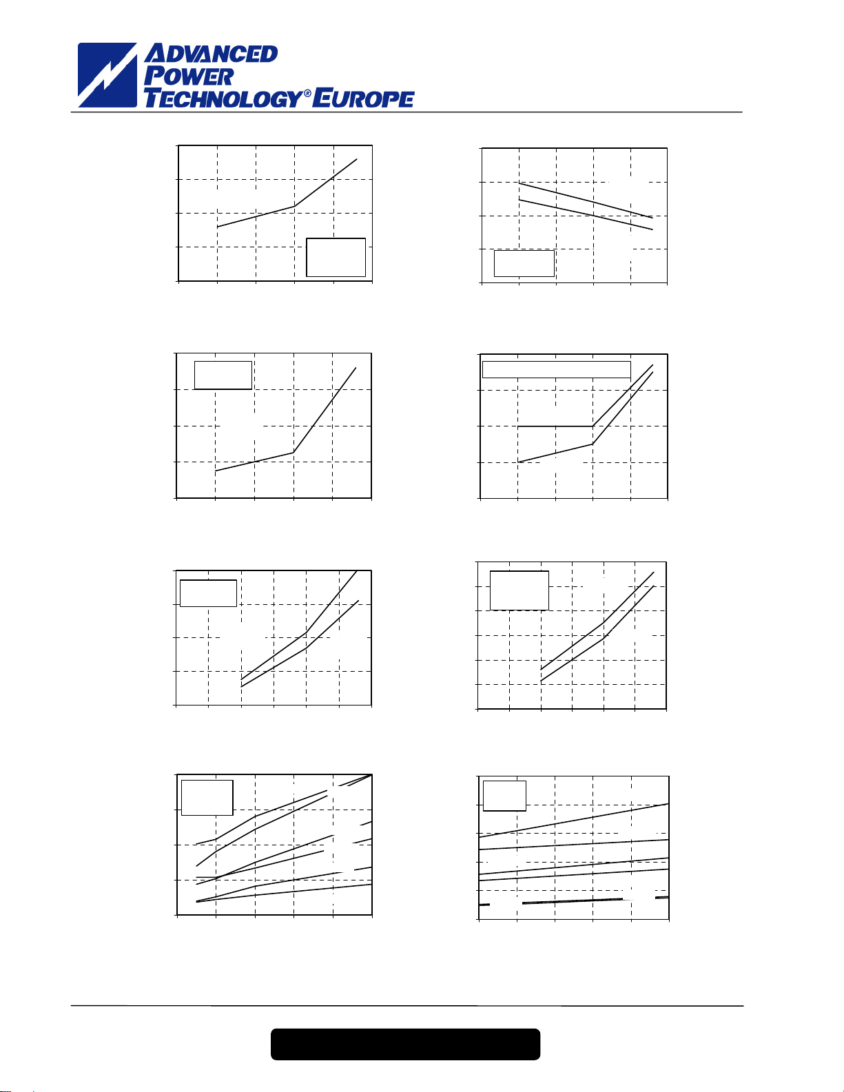
Turn-On Delay Time vs Collector Current
35
30
VGE = 15V
25
20
td(on), Turn-On Delay Time (ns)
15
Tj = 25°C
V
= 400V
CE
= 5Ω
R
G
25 50 75 100 125 150
, Collector to Emitter Current (A)
I
CE
Current Rise Time vs Collector Current
80
VCE = 400V
= 5Ω
R
60
40
tr, Rise Time (ns)
20
G
VGE=15V,
=125°C
T
J
0
25 50 75 100 125 150
I
, Collector to E mitter Current (A)
CE
Turn-Off Delay Time vs Collector Current
250
200
VGE=15V,
=125°C
T
J
150
100
VCE = 400V
= 5Ω
R
G
50
td(off), Turn-Off Delay Time (ns)
25 50 75 100 125 150
VGE=15V,
=25°C
T
J
ICE, Collector to E mitter Current (A)
Current Fall Time vs Collector Current
80
VCE = 400V, VGE = 15V, RG = 5Ω
60
TJ = 125°C
40
tf, Fall Time (ns)
20
TJ = 25°C
0
25 50 75 100 125 150
ICE, Collector to Emitter Current (A)
Turn-On Energy Loss vs Collector Current
8
VCE = 400V
= 5Ω
R
G
6
4
TJ=125°C,
=15V
V
GE
TJ=25°C,
=15V
V
GE
2
, Turn-On Energy Loss (mJ)
on
0
E
0 25 50 75 100 125 15 0
, Collector to Emitter Current (A)
I
CE
Switching Energy Losses vs Gate Resistance
16
12
8
VCE = 400V
= 15V
V
GE
= 125°C
T
J
Eon, 200A
Eoff, 200A
Eoff, 100A
Eon, 100A
Eoff, 50A
4
Eon, 50A
Switching Energy Losses (mJ)
0
0 1020304050
Gate Resistance (Ohms)
Turn-Off Energy Loss vs Collector Current
6
5
4
3
VCE = 400V
= 15V
V
GE
= 5Ω
R
G
TJ = 125°C
TJ = 25°C
2
1
, Turn-off Energy Loss (mJ)
off
E
0
0 255075100125150
, Collector to E mitter Current (A)
I
CE
Switching Energy Losses vs Junction Temp.
10
VCE = 400V
= 15V
V
GE
8
R
= 5Ω
G
6
Eon, 10 0A
4
2
Eoff, 50A
Switching Energy Losses (mJ)
0
0 255075100125
T
, Junction Temperature (°C)
J
Eon, 200A
Eoff, 20 0A
Eoff, 100A
Eon, 50A
APT website –http://www.advancedpower.com
5-9
APT100GF60JU3– Rev 0 April, 2004

APT100GF60JU3
Capacitanc e vs Collector to Emi tter Vol tage
10000
Cies
1000
Coes
C, Capacitance (pF)
100
0 1020304050
V
, Collector to Emitter Voltage (V)
CE
Maximum Effecti ve Transient Thermal Impedance, Junc tion to Cas e vs Pulse Duration
0.35
0.3
0.9
0.25
0.7
0.2
0.5
0.15
0.3
0.1
0.05
Thermal Impedance (°C/W)
0.1
0.05
0
0.00001 0. 0001 0.001 0.01 0.1 1 10
Cres
Single Pulse
Rectangular Pulse Duration (Seconds)
Minimum Switching Safe Operating Area
350
300
250
200
150
100
, Collector Current (A)
C
I
50
0
0 200 400 6 00 800
V
, Collector to Emitter Voltage (V)
CE
Operating Frequency vs Collector Current
120
100
80
60
40
20
0
Fmax, Operating Frequency (kHz)
20 40 60 80 100 120
I
, Collector Current (A)
C
VCE = 400V
D = 50%
R
G
T
J
= 5Ω
= 125°C
APT website –http://www.advancedpower.com
6-9
APT100GF60JU3– Rev 0 April, 2004

APT100GF60JU3
Typical Diode Performance Curve
APT website –http://www.advancedpower.com
7-9
APT100GF60JU3– Rev 0 April, 2004

APT100GF60JU3
APT website –http://www.advancedpower.com
8-9
APT100GF60JU3– Rev 0 April, 2004

APT100GF60JU3
SOT-227 (ISOTOP®) Package Outline
11.8 (.463)
31.5 (1.240)
31.7 (1.248)
W=4.1 (.161)
W=4.3 (.169)
H=4.8 (.187)
H=4.9 (.193)
(4 places)
4.0 (.157)
4.2 (.165)
(2 places)
3.3 (.129)
3.6 (.143)
Anode
r = 4.0 (.157)
(2 places)
7.8 (.307)
8.2 (.322)
14.9 (.587)
15.1 (.594)
30.1 (1.185)
30.3 (1.193)
38.0 (1.496)
38.2 (1.504)
Emitter
Dimensions in Millimeters and (Inches)
12.2 (.480)
8.9 (.350)
9.6 (.378)
0.75 (.030)
0.85 (.033)
1.95 (.077)
2.14 (.084)
Hex Nut M4
(4 places)
25.2 (0.992)
12.6 (.496)
12.8 (.504)
25.4 (1.000)
Collector
*
Emitter terminals are shorted
internally. Current handling
capability is equal for either
Emitter terminal.
Gate
ISOTOP® is a Registered Trademark of SGS Thomson
APT reserves the right to change, without notice, the specifications and information contained herein
APT's products are covere d by one or more of U.S patents 4,895, 810 5,045,903 5,0 89,434 5,182, 234 5,019, 522
5,262,3 36 6, 503,786 5,256,5 83 4,7 48,103 5,283,20 2 5,23 1,474 5,434,095 5,528 ,058 and f oreign patents. U .S and Forei gn patents pe ndin g. All Rights Reserved.
APT website –http://www.advancedpower.com
9-9
APT100GF60JU3– Rev 0 April, 2004
 Loading...