

查询APT10050B2LC供应商
APT10050B2LC
APT10050LLC
1000V 21A 0.500W
POWER MOS VI
TM
Power MOS VITM is a new generation of low gate charge, high voltage
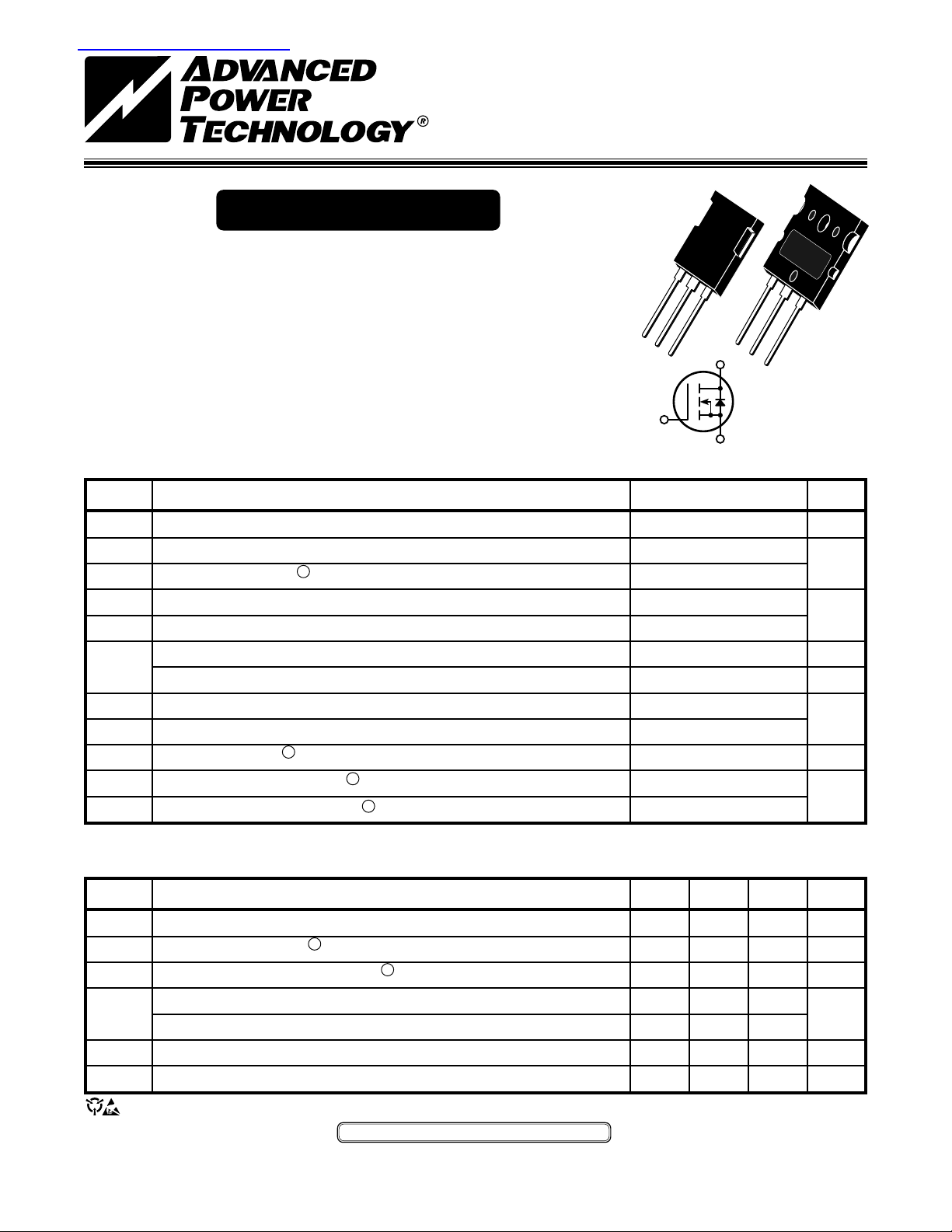
B2LC
T-MAX™
TO-264
N-Channel enhancement mode power MOSFETs. Lower gate charge is
achieved by optimizing the manufacturing process to minimize C
TM
Lower gate charge coupled with Power MOS VI
optimized gate layout,
delivers exceptionally fast switching speeds.
• Identical Specifications: T-MAX™ or TO-264 Package
• Lower Gate Charge & Capacitance • Easier To Drive
and C
iss
rss
.
LLC
D
G
• 100% Avalanche Tested • Faster switching
S
MAXIMUM RATINGS All Ratings: TC = 25°C unless otherwise specified.
Symbol
V
DSS
I
D
I
DM
V
GS
V
GSM
P
D
TJ,T
STG
T
L
I
AR
E
AR
E
AS
Parameter
Drain-Source Voltage
Continuous Drain Current @ T
Pulsed Drain Current
Gate-Source Voltage Continuous
Gate-Source Voltage Transient
Total Power Dissipation @ T
Linear Derating Factor
Operating and Storage Junction Temperature Range
Lead Temperature: 0.063" from Case for 10 Sec.
Avalanche Current
Repetitive Avalanche Energy
Single Pulse Avalanche Energy
ADVANCED TECHNICAL
1
1
(Repetitive and Non-Repetitive)
= 25°C
C
= 25°C
C
1
4
INFORMATION
APT10050
1000
21
84
±30
±40
520
4.16
-55 to 150
300
21
50
2500
UNIT
Volts
Amps
Volts
Watts
W/°C
°C
Amps
mJ
STATIC ELECTRICAL CHARACTERISTICS
Symbol
BV
I
D(on)
R
DS(on)
I
DSS
I
GSS
V
GS(th)
USA 405 S.W. Columbia Street Bend, Oregon 97702-1035 Phone: (541) 382-8028 FAX: (541) 388-0364
EUROPE Chemin de Magret F-33700 Merignac - France Phone: (33)5 579215 15 FAX: (33)5 56 47 9761
Characteristic / Test Conditions
Drain-Source Breakdown Voltage (V
DSS
On State Drain Current
Drain-Source On-State Resistance
Zero Gate Voltage Drain Current (VDS = V
Zero Gate Voltage Drain Current (V
Gate-Source Leakage Current (VGS = ±30V, V
Gate Threshold Voltage (VDS = VGS, ID = 2.5mA)
CAUTION: These Devices are Sensitive to Electrostatic Discharge. Proper Handling Procedures Should Be Followed.
2
(V
DS
APT Website - http://www.advancedpower.com
= 0V, ID = 250µA)
GS
> I
x R
D(on)
2
(VGS = 10V, 0.5 I
DSS
= 0.8 V
DS
Max, VGS = 10V)
DS(on)
D[Cont.]
, VGS = 0V)
, VGS = 0V, TC = 125°C)
DSS
= 0V)
DS
)
MIN TYP MAX
1000
21
35
0.500
25
250
±100
UNIT
Volts
Amps
Ohms
µA
nA
Volts
050-5929 rev A 8-2000
DYNAMIC CHARACTERISTICS APT10050 B2LC - LLC
Symbol
C
C
C
Q
Q
Q
t
d(on)
t
d(off)
Characteristic
Input Capacitance
iss
Output Capacitance
oss
Reverse Transfer Capacitance
rss
Total Gate Charge
g
Gate-Source Charge
gs
Gate-Drain ("Miller") Charge
gd
Turn-on Delay Time
t
Rise Time
r
Turn-off Delay Time
t
Fall Time
f
Test Conditions
V
VDS = 25V
f = 1 MHz
3
V
GS
VDD = 0.5 V
ID = 0.5 I
VGS = 15V
VDD = 0.5 V
ID = I
D[Cont.]
RG = 0.6W
SOURCE-DRAIN DIODE RATINGS AND CHARACTERISTICS
Symbol
I
I
SM
V
t
Q
Characteristic / Test Conditions
Continuous Source Current (Body Diode)
S
1
Pulsed Source Current
Diode Forward Voltage 2 (VGS = 0V, IS = -I
SD
rr
rr
ADVANCED TECHNICAL
Reverse Recovery Time (IS = -I
Reverse Recovery Charge (I
(Body Diode)
INFORMATION
S
= -I
, dlS/dt = 100A/µs)
D[Cont.]
, dlS/dt = 100A/µs)
D[Cont.]
D[Cont.]
)
= 0V
GS
= 10V
D[Cont.]
DSS
@ 25°C
DSS
@ 25°C
MIN TYP MAX
5000
600
190
170
30
95
18
13
43
8.5
MIN TYP MAX
21
84
1.3
960
22.0
UNIT
pF
nC
ns
UNIT
Amps
Volts
ns
µC
THERMAL CHARACTERISTICS
Symbol
R
qJC
R
qJA
1
Repetitive Rating: Pulse width limited by maximum junction
temperature.
2
Pulse Test: Pulse width < 380 µS, Duty Cycle < 2%
APT Reserves the right to change, without notice, the specifications and information contained herein.
APT's devices are covered by one or more of the following U.S.patents: 4,895,810 5,045,903 5,089,434 5,182,234 5,019,522 5,262,336
050-5929 rev A 8-2000
Characteristic
Junction to Case
Junction to Ambient
T-MAXTM (B2) Package Outline
4.69 (.185)
5.31 (.209)
1.49 (.059)
2.49 (.098)
20.80 (.819)
Drain
0.40 (.016)
0.79 (.031)
2.21 (.087)
2.59 (.102)
These dimensions are equal to the TO-247 without the mounting hole.
21.46 (.845)
4.50 (.177) Max.
19.81 (.780)
20.32 (.800)
1.01 (.040)
1.40 (.055)
5.45 (.215) BSC
Dimensions in Millimeters and (Inches)
15.49 (.610)
16.26 (.640)
2-Plcs.
5,256,583 4,748,103 5,283,202 5,231,474 5,434,095 5,528,058
3
See MIL-STD-750 Method 3471
4
Starting T
+25°C, L = 41.32mH, R
j
=
TO-264 (L) Package Outline
4.60 (.181)
5.21 (.205)
1.80 (.071)
5.38 (.212)
6.20 (.244)
2.87 (.113)
3.12 (.123)
1.65 (.065)
2.13 (.084)
Gate
Drain
Source
Drain
2.01 (.079)
0.48 (.019)
0.84 (.033)
2.59 (.102)
3.00 (.118)
Dimensions in Millimeters and (Inches)
5.79 (.228)
6.20 (.244)
25.48 (1.003)
26.49 (1.043)
2.29 (.090)
2.69 (.106)
19.81 (.780)
21.39 (.842)
0.76 (.030)
1.30 (.051)
5.45 (.215) BSC
MIN TYP MAX
0.24
40
25W, Peak IL = 21A
G
=
19.51 (.768)
2.79 (.110)
3.18 (.125)
2-Plcs.
20.50 (.807)
3.10 (.122)
3.48 (.137)
2.29 (.090)
2.69 (.106)
Gate
Drain
Source
UNIT
°C/W
 Loading...