

D
G
S
TO-247
APT1001R1BN 1000V 10.5A 1.10Ω
APT1001R3BN 1000V 10.0A 1.30Ω
POWER MOS IV
N-CHANNEL ENHANCEMENT MODE HIGH VOLTAGE POWER MOSF ETS
MAXIMUM RATINGS All Ratings: T
Symbol
V
I
V
P
TJ,T
DSS
I
D
DM
GS
D
STG
T
L
Parameter
Drain-Source Voltage
Continuous Drain Current @ T
Pulsed Drain Current
Gate-Source Voltage
Total Power Dissipation @ T
Linear Derating Factor
Operating and Storage Junction Temperature Range
Lead Temperature: 0.063" from Case for 10 Sec.
®
= 25°C unless otherwise specified.
C
APT APT
1001RBN 1001R3BN
1000 1000
= 25°C
C
1
10.5 10
42 40
±30
= 25°C
C
310
2.48
-55 to 150
300
UNIT
Volts
Amps
Volts
Watts
W/°C
°C
STATIC ELECTRICAL CHARACTERISTICS
Symbol
BV
ID(ON)
R
DS
I
DSS
I
GSS
VGS(TH)
Characteristic / Test Conditions / Part Number
Drain-Source Breakdown Voltage
DSS
(V
= 0V, ID = 250 µA)
GS
On State Drain Current
(V
> ID(ON) x RDS(ON) Max, VGS = 10V)
DS
Drain-Source On-State Resistance
(ON)
(VGS = 10V, 0.5 ID [Cont.])
2
Zero Gate Voltage Drain Current (V
Zero Gate Voltage Drain Current (V
Gate-Source Leakage Current (V
Gate Threshold Voltage (V
= VGS, ID = 1.0mA)
DS
2
= V
DS
= 0.8 V
DS
= ±30V, V
GS
, VGS = 0V)
DSS
, VGS = 0V, TC = 125°C)
DSS
= 0V)
DS
MIN TYP MAX
APT1001R1BN
1000
APT1001R3BN 1000
APT1001R1BN 10.5
APT1001R3BN 10
APT1001R1BN 1.10
APT1001R3BN 1.30
250
1000
±100
24
UNIT
Volts
Amps
Ohms
µA
nA
Volts
THERMAL CHARACTERISTICS
Symbol
R
R
USA
405 S.W. Columbia Street Bend, Oregon 97702-1035 Phone: (541) 382-8028 FAX: (541) 388-0364
EUROPE
Avenue J.F. Kennedy Bât B4 Parc Cadéra Nord F-33700 Merignac - France Phone: (33)5 57 92 15 15 FAX: (33) 5 56 47 97 61
Characteristic
Junction to Case
θJC
Junction to Ambient
θJA
CAUTION: These Devices are Sensitive to Electrostatic Discharge. Proper Handling Procedures Should Be Followed.
MIN TYP MAX
UNIT
0.40
°C/W
40
050-0007 Rev C
DYNAMIC CHARACTERISTICS
APT1001R1/1001R3BN
Symbol
C
iss
C
oss
C
rss
Q
g
Q
gs
Q
gd
td(on)
t
r
td(off)
t
f
Characteristic
Input Capacitance
Output Capacitance
Reverse Transfer Capacitance
Total Gate Charge
3
Gate-Source Charge
Gate-Drain ("Miller") Charge
Turn-on Delay Time
Rise Time
Turn-off Delay Time
Fall Time
Test Conditions
V
VDS = 25V
f = 1 MHz
V
GS
VDD = 0.5 V
ID = ID [Cont.] @ 25°C
V
GS
VDD = 0.5 V
ID = ID [Cont.] @ 25°C
RG = 1.8Ω
SOURCE-DRAIN DIODE RATINGS AND CHARACTERISTICS
I
SM
t
Characteristic / Test Conditions / Part Number
Continuous Source Current
S
(Body Diode)
Pulsed Source Current
1
(Body Diode)
2
Diode Forward Voltage
SD
Reverse Recovery Time (I
rr
Reverse Recovery Charge (I
rr
(VGS = 0V, IS = -ID [Cont.])
= -ID [Cont.], dlS/dt = 100A/µs)
S
= -ID [Cont.], dlS/dt = 100A/µs)
S
Symbol
I
V
Q
MIN TYP MAX
GS
= 0V
2460 2950
360 500
105 160
= 10V
DSS
90 130
9.3 14
47 70
= 15V
DSS
15 30
16 32
64 95
24 48
MIN TYP MAX
APT1001R1BN
APT1001R3BN 10
APT1001R1BN 42
APT1001R3BN 40
636 1200
4.5 11
10.5
1.3
UNIT
pF
nC
ns
UNIT
Amps
Volts
ns
µC
SAFE OPERATING AREA CHARACTERISTICS
Symbol
SOA1
SOA2
I
1
Repetitive Rating: Pulse width limited by maximum junction temperature. See Transient Thermal Impedance Curve. (Fig.1)
2
Pulse Test: Pulse width < 380 µS, Duty Cycle < 2%
3
See MIL-STD-750 Method 3471
APT Reserves the right to change, without notice, the specifications and information contained herein.
050-0007 Rev C
Characteristic
Safe Operating Area
Safe Operating Area
Inductive Current Clamped
LM
1.0
0.5
D=0.5
0.2
0.1
0.05
0.02
0.01
-5
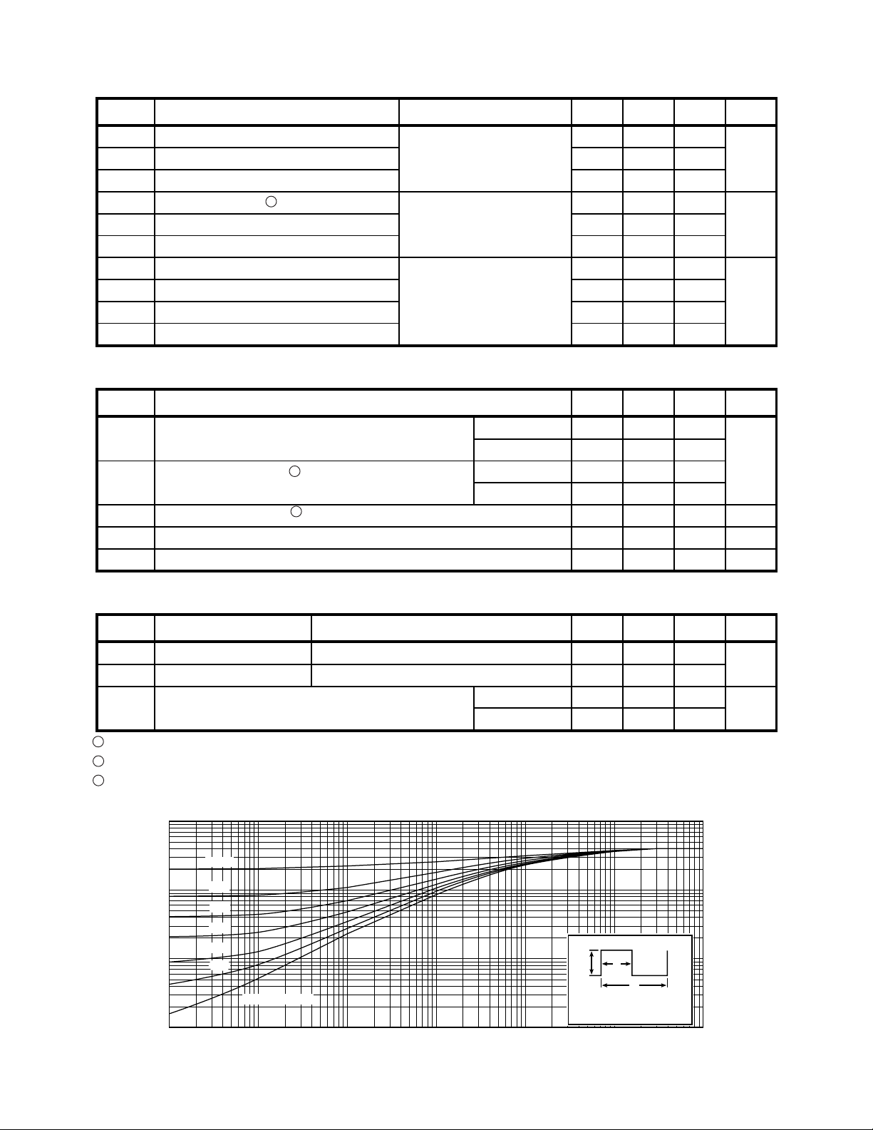
FIGURE 1, MAXIMUM EFFECTIVE TRANSIENT THERMAL IMPEDANCE, JUNCTION-TO-CASE vs PULSE DURATION
, THERMAL IMPEDANCE (°C/W)
JC
θ
Z
0.1
0.05
0.01
0.005
0.001
10
SINGLE PULSE
-4
10
Test Conditions / Part Number
V
= 0.4 V
DS
= ID [Cont.], VDS = PD / ID [Cont.], t = 1 Sec.
I
DS
, IDS = PD / 0.4 V
DSS
, t = 1 Sec.
DSS
APT1001R1BN 42
APT1001R3BN 40
-3
10
RECTANGULAR PULSE DURATION (SECONDS)
-2
10
10
MIN TYP MAX
310
310
Note:
DM
P
Duty Factor D =
Peak TJ = PDM x Z
-1
1.0 10
UNIT
Watts
Amps
t
1
t
2
t
1
/
t
2
+ T
θJC
C

APT1001R1/1001R3BN
16
VGS=10V
12
6V
5.5V
16
VGS=10V
12
6V
5.5V
8
8
5V
4
, DRAIN CURRENT (AMPERES)
D
0
0 100 200 300 400 500
VDS, DRAIN-TO-SOURCE VOLTAGE (VOLTS) VDS, DRAIN-TO-SOURCE VOLTAGE (VOLTS)
4.5V
4V
4
, DRAIN CURRENT (AMPERES)
D
0
0 4 8 12 16 20
FIGURE 2, TYPICAL OUTPUT CHARACTERISTICS FIGURE 3, TYPICAL OUTPUT CHARACTERISTICS
20
16
V > I (ON) x R (ON)MAX.
DS D DS
230µ SEC. PULSE TEST
TJ = -55°C
TJ = +25°C
TJ = +125°C
12
8
4
, DRAIN CURRENT (AMPERES) I
D
0
FIGURE 4, TYPICAL TRANSFER CHARACTERISTICS FIGURE 5, R
TJ = +125°C
TJ = +25°C
0 2 4 6 8
V
, GATE-TO-SOURCE VOLTAGE (VOLTS) ID, DRAIN CURRENT (AMPERES)
GS
TJ = -55°C
12
2.5
2.0
1.5
TJ = 25°C
2µ SEC. PULSE TEST
NORMALIZED TO
= 10V @ 0.5 ID [Cont.]
V
GS
VGS=10V
1.0
0.5
(ON), DRAIN-TO-SOURCE ON RESISTANCE I
0.0
DS
0 6 12 18 24 30
(ON) vs DRAIN CURRENT
DS
1.2
VGS=20V
5V
4.5V
4V
10
8
APT1001R1BN
1.1
1.0
APT1001R3BN
6
0.9
4
, DRAIN CURRENT (AMPERES) I
2
D
0
25 50 75 100 125 150
T
, CASE TEMPERATURE (°C) TJ, JUNCTION TEMPERATURE (°C)
FIGURE 6, MAXIMUM DRAIN CURRENT vs CASE TEMPERATURE FIGURE 7, BREAKDOWN VOLTAGE vs TEMPERATURE
2.5
C
ID = 0.5 ID [Cont.]
VGS = 10V
2.0
1.5
1.0
(NORMALIZED)
0.5
(ON), DRAIN-TO-SOURCE ON RESISTANCE I
0.0
DS
-50 -25 0 25 50 75 100 125 150
R
T
, JUNCTION TEMPERATURE (°C) TC, CASE TEMPERATURE (°C)
J
FIGURE 8, ON-RESISTANCE vs. TEMPERATURE FIGURE 9, THRESHOLD VOLTAGE vs TEMPERATURE
0.8
(ON), DRAIN-TO-SOURCE BREAKDOWN R
DSS
0.7
-50 -25 0 25 50 75 100 125 150
1.4
1.2
1.0
0.8
(NORMALIZED) VOLTAGE (NORMALIZED)
(TH), THRESHOLD VOLTAGE BV
0.6
GS
V
0.4
-50 -25 0 25 50 75 100 125 150
050-0007 Rev C

60
10
APT1001R1BN
APT1001R3BN
OPERATION HERE
LIMITED BY R
APT1001R1BN
APT1001R3BN
(ON)
DS
10µS
100µS
1mS
10mS
1
, DRAIN CURRENT (AMPERES)
D
TC =+25°C
TJ =+150°C
SINGLE PULSE
100mS
DC
APT1001R1/1001R3BN
.1
1 5 10 50 100 1000
VDS, DRAIN-TO-SOURCE VOLTAGE (VOLTS) VDS, DRAIN-TO-SOURCE VOLTAGE (VOLTS)
FIGURE 10, MAXIMUM SAFE OPERATING AREA FIGURE 11, TYPICAL CAPACITANCE vs DRAIN-TO-SOURCE VOLTAGE
20
ID = ID [Cont.]
16
12
VDS=100V
VDS=200V
VDS=500V
8
10,000
C
iss
1,000
C
oss
C
100
10
0 10 20 30 40 50
rss
100
50
20
TJ = +150°C TJ = +25°C
10
5
APT1001R1/1001R3BN
4
, GATE-TO-SOURCE VOLTAGE (VOLTS) I
GS
V
0
0 40 80 120 160 200
Q
, TOTAL GATE CHARGE (nC) VSD, SOURCE-TO-DRAIN VOLTAGE (VOLTS)
FIGURE 12, GATE CHARGES vs GATE-TO-SOURCE VOLTAGE FIGURE 13, TYPICAL SOURCE-DRAIN DIODE FORWARD VOLTAGE
g
2
, REVERSE DRAIN CURRENT (AMPERES) C, CAPACITANCE (pF)
DR
1
I
0 .5 1.0 1.5 2.0
TO-247AD Package Outline
4.69 (.185)
Drain
5.31 (.209)
1.49 (.059)
2.49 (.098)
0.40 (.016)
0.79 (.031)
6.15 (.242) BSC
20.80 (.819)
21.46 (.845)
4.50 (.177) Max.
19.81 (.780)
20.32 (.800)
1.01 (.040)
1.40 (.055)
15.49 (.610)
16.26 (.640)
5.38 (.212)
6.20 (.244)
3.55 (.140)
3.81 (.150)
2.87 (.113)
3.12 (.123)
1.65 (.065)
2.13 (.084)
Gate
Drain
Source
050-0007 Rev C
2.21 (.087)
2.59 (.102)
5.45 (.215) BSC
2-Plcs.
Dimensions in Millimeters and (Inches)
 Loading...