

http://www.BDTIC.com/AMS
Advanced AMS5105
Monolithic 500mA CMOS LOW DROPOUT VOLTAGE REGULATOR
Systems
RoHS compliant
FEATURES APPLICATIONS
• Fixed and Adjustable Versions Available • Cellular Telephones
• Output Current up to 500mA • Portable Consumer Equipment
• Very Low Quiescent Current • Portable (Notebook) Computers
• Input-output Differential less than 0.5V • Battery Powered Systems
• Short Circuit Protection • Portable Instrumentation
• Internal Thermal Overload Protection • Radio Control Systems
• ENABLE Pin available in selected packages • CD/DVD drives
GENERAL DESCRIPTION
The AMS5105 series consists of positive fixed and adjustable voltage regulators ideally suited for use in battery-powered
systems. These devices feature very low quiescent current (500uA or less) when supplying loads up to 500mA, and a standby
current less than 500nA when disabled using the ENABLE pin (available in selected packages). These unique characteristics
and the low input-output differential required for proper regulation (0.5V for output currents of 500mA) make the AMS5105
ideal for use in standby power systems. Internal current limiting and thermal shutdown features provide protection for all
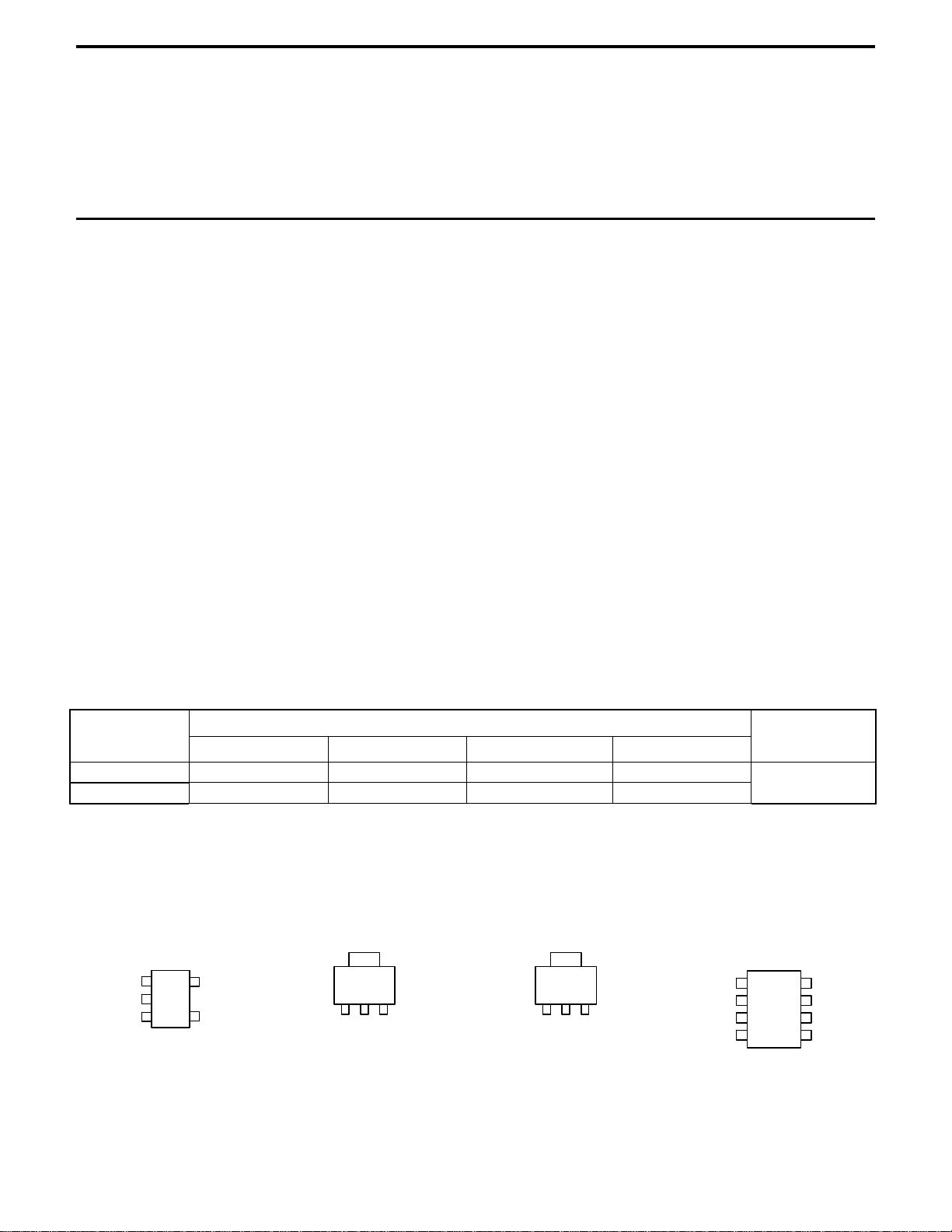
AMS5105 series devices regardless of package type. The AMS5105 is offered as fixed voltage regulators in the 5 lead SOT-23,
SOT-89, SOT-223, and 8 lead SOIC packages, and as adjustable voltage regulators in the 5 lead SOT-23 and 8 lead SOIC
packages. All devices in the 5 lead SOT-23 and 8 lead SOIC packages are provided with ENABLE pin.
ORDERING INFORMATION
OUTPUT PACKAGE TYPE TEMP.
VOLTAGE
5L SOT-23 SOT-89 SOT-223 SO-8
FIXED AMS5105M1-X AMS5105L-X AMS5105-X AMS5105S-X -25C to 125C
ADJUSTABLE AMS5105M1 AMS5105S -25C to 125C
X = 1.5V, 1.8V, 2.5V, 2.8V, 3.3V.
PIN CONNECTIONS
5 Lead SOT-23
(M1)
V
GROUND
ENABLE
1
IN
2
3
5
V
OUT
FB
4
N/C
Top View Top View Top View Top View
V
OUT
SOT-89
(L)
123
GND
V
IN
V
OUT
SOT-223
123
GND
V
RANGE
8 Lead SOIC
(S)
V
1
OUT
2
GROUND
3
IN
GROUND
FB
N/C
4
V
8
7
GROUND
GROUND
6
ENABLE
5
IN
N/C
Advanced Monolithic Systems, Inc.
http://www.BDTIC.com/AMS
AMS5105
ABSOLUTE MAXIMUM RATINGS
Input Supply Voltage -0.3 to +6.5V Maximum Junction Temperature
Internal Power Dissipation (Note 4) Internally Limited Storage Temperature
ESD 2000V Lead Temperature (Soldering 25 sec)
ELECTRICAL CHARACTERISTICS
Electrical Characteristics at V
PARAMETER
Fixed Output Voltage Versions
Output Voltage Tolerance -1.5 +1.5 %
Line Regulation
Load Regulation
Dropout Voltage
Quiescent Current
Maximum Operational Input
Voltage
ENABLE Threshold Voltage
Enabled
Disabled
ENABLE Threshold Current V
Wake-Up Response Time
(from disabled state)
IN =VOUT
(V
+1V) ≤ VIN ≤6V, I
OUT
-25°C ≤T
(V
+1V) ≤VIN ≤ 6V
IN
1mA ≤I
5mA ≤ I
= 10 mA
I
OUT
I
= 100 mA
OUT
= 500 mA
I
OUT
= 10 mA
I
OUT
= 100 mA
I
OUT
I
= 500 mA
OUT
R
= 500Ω, In disabled state, V
L
6 V
VIN = 3V to 6V (Note 6)
ENABLE
(Note 7) - 20 30
(Note 1)
+125°C
-65°C to +150°C
+1V, I
CONDITIONS
≤125°C
J
≤ 100 mA
OUT
≤ 500 mA
OUT
= 0.6 x VIN, VIN = 3V to 6V 0.01 1 nA
=1mA, TJ=25°C, C
OUT
=100 mA
OUT
ENABLE
= 0
= 2.2µF unless otherwise specified.
OUT
AMS5105-X
Min. Typ. Max.
- 3.0
30
60
5
8
50
20
100
400
450
450
450
100
-
-
+ 3.0
10
30
50
70
25
125
500
550
550
550
500
15
Units
%
mV/V
mV/V
mV
mV
mV
mV
mV
µA
µA
µA
nA
% V
% V
µs
265°C
IN
IN
Advanced Monolithic Systems, Inc.
http://www.BDTIC.com/AMS
AMS5105
ELECTRICAL CHARACTERISTICS
Electrical Characteristics at V
PARAMETER
Adjustable Version
Reference Voltage
Output Voltage Range 1.25 - 5 V
Line Regulation
Load Regulation
Dropout Voltage
Quiescent Current
Maximum Operational Input
Voltage
ENABLE Threshold Voltage
Enabled
Disabled
ENABLE Threshold Current V
Wake-Up Response Time
(from disabled state)
Note 1: Absolute Maximum Ratings are limits beyond which damage to the device may occur. For guaranteed performance limits and associated test
conditions, see the Electrical Characteristics tables.
Note 2: To ensure constant junction temperature, low duty cycle pulse testing is used.
Note 3: Limits appearing in boldface type apply over the entire junction temperature range for operation. Limits appearing in normal type apply for
T
= TJ = 25°C.
A
Note 4: The maximum allowable power dissipation is a function of the maximum junction temperature T
and the ambient temperature TA. The maximum allowable power dissipation at any ambient temperature is calculated using:
P(MAX)
Where the values of the junction-to-ambient thermal resistances are as follows: 220°C/W for 5 lead SOT-23 (M1) and 160°C/W for the molded plastic SO-8 (S).
Note 5: Dropout Voltage is defined as the input to output differential at which the output voltage drops 100mV below its nominal value measured at 1V
differential.
Note 6:
ENABLE Threshold Voltage levels are specified as a percentage of input voltage V
equal to V
Note 7: Time required for V
.
IN
OUT
IN
=6V, V
OUT
=3V, I
=1mA, TJ=25°C, C
OUT
CONDITIONS
(Note 2)
= 2.2µF unless otherwise specified.
OUT
Min.
AMS5105
Typ.
Max.
Units
1.231 1.250 1.269 V
≤ 100 mA, -25°C ≤T
I
OUT
Measured from FB pin to
+ 1V ≤VIN ≤ 6V
V
OUT
1mA ≤I
5mA ≤I
I
I
I
I
I
I
R
≤ 100 mA
O
≤ 500 mA
O
≤ 10 mA
OUT
= 100 mA
OUT
= 500 mA (Note 5)
OUT
= 10 mA
OUT
= 100 mA
OUT
= 500 mA
OUT
= 500Ω, In disabled state, V
L
V
= 3V to 6V (Note 6)
IN
= 0.6 x VIN, VIN = 3V to 6V 0.01 1 nA
ENABLE
(Note 7) - 20 30
≤ 125°C
J
GROUND
ENABLE
= 0
1.218 1.250 1.282
V
- 1.5 %
0.3 1 1
20
100
400
350
350
350
100
25
125
500
450
450
450
500
2
%
%
mV
mV
mV
µA
µA
µA
nA
6 V
60
-
-
-
-
15
% V
% V
IN
IN
µs
(MAX), the junction-to ambient thermal resistance θ
J
AJ
=
θ
to reach 95% of output voltage setting after V
T-(MAX)T
Aθ-J
. Quiescent current can be minimized by choosing V
IN
is switched from 0V to V
ENABLE
.
IN
ENABLE
HIGH
J-A
Advanced Monolithic Systems, Inc.

http://www.BDTIC.com/AMS
TYPICAL PERFORMANCE CHARACTERISTICS
AMS5105
Advanced Monolithic Systems, Inc.

http://www.BDTIC.com/AMS
AMS5105
AMS5105/-X Pin Description 5-Lead SOT-23
PIN NAME DESCRIPTION
1 VIN Unregulated input voltage
Connect C
2 GND Ground connection for VIN
and V
3 ENABLE Logical high enables regulator
Logical low disables regulator
4 FB Feedback from resistor divider
Used to set output voltage
Adjustable versions only
(See Figures 3 and 4)
5 V
Regulated output voltage
OUT
Connect C
GND
from VIN to GND
IN
OUT
from V
OUT
OUT
to
Advanced Monolithic Systems, Inc.

http://www.BDTIC.com/AMS
APPLICATION NOTES
Definition of Terms
Dropout Voltage
the circuit stops to regulate against further reduction in input
voltage. Measured when the output voltage has dropped 100mV
from the nominal voltage obtained at 1V input, dropout voltage is
dependent upon load current and junction temperature.
Input Voltage: The DC voltage applied to the input terminal with
respect to ground.
Input-Output Differential: The voltage difference between the
unregulated input voltage and the regulated output voltage for
which the regulator will regulate.
Line Regulation: The change in output voltage for a change in
the input voltage. The line regulation is measured under conditions
of low dissipation or by using low duty cycle pulse testing such
that the average chip temperature is not significantly affected.
Load Regulation: The change in output voltage for a change in
load current at constant chip temperature.
Long term stability: Output voltage stability under accelerated
life-test conditions after 1000 hours with maximum rated voltage
and junction temperature.
Quiescent Current: That part of the positive input current that
does not contribute to the positive load current. The regulator
ground lead current.
Temperature Stability of V
voltage for a thermal variation from room temperature to either
temperature extreme.
External capacitor
The AMS5105 series requires an output capacitor of 2.2µF or
greater to ensure device stability, as shown in Figures 1 through 4.
Without the capacitor the device may oscillate. Most types of
tantalum or electrolytic capacitor can be used in the applications.
The value of this capacitor can be increased without limits. For
: The input-output voltage differential at which
: The percentage change in output
O
AMS5105
higher loads, the value of the capacitor should be increased,
especially when the output voltage is set for 2.5V or less. The
AMS5105 lowest fixed output voltage value is 1.5V.
Programming the Output Voltage
The AMS5105 may be programmed for any output voltage
between its 1.25V reference and its 6V maximum rating, allowing
for dropout and power dissipation. As shown in Figure 3, an
external pair of resistors is required.
The equation for the output voltage is:
VOUT = VREF ⋅ (1 + R1/ R2)
where V
Typical application circuit (adjustable output)
REF is the nominal 1.25 reference voltage.
TYPICAL APPLICATION
+V
IN
+
2.2 F
C
IN
3
+V
IN
V
AMS5105-X
GND
2
OUT
V
OUT
1
2.2 F
+
C
OUT
Figure 1
Advanced Monolithic Systems, Inc.
+
2.2 F
C
IN
3
ENABLE
GND
Figure 2
+V
IN
1
+V
IN
V
AMS5105-X
2
OUT
+V
IN
2.2 F
V
5
OUT
2.2
F
+
C
OUT
+
C
IN
3
Figure 3
1
+V
IN
AMS5105
ENABLE
GND FB
V
+
OUT
2.2 F
C
OUT
5
V
OUT
R
1
42
1.25V
R
V
REF
2

http://www.BDTIC.com/AMS
PACKAGE DIMENSIONS inches (millimeters) unless otherwise noted.
5 LEAD SOT-23 PLASTIC PACKAGE (M1)
0.110-0.120
(2.794-3.048)
0.102-0.118
(2.60-3.00)
0.059-0.070
(1.50-1.75)
AMS5105
0.155-0.167
(3.94-4.25)
0.090-0.102
(2.29-2.60)
0.018-0.024
(0.457-0.610)
0.036-0.051
(0.090-1.30)
0.003
(0.150)
MAX
0.037
(0.95)
TYP
0.173-0.181
(4.40-4.60)
0.064-0.072
(1.62-1.83)
0.014-0.020
(0.350-0.50)
10°
NOM
0.075
(1.90)
TYP
10°
NOM
SOT-89 PLASTIC PACKAGE (L)
0.055-0.063
(1.40-1.60)
0.084-0.090
(2.13-2.29)
0.018-0.024
(0.457-0.610)
0.014-0.017
(0.35-0.44)
0.0035-0.0080
(0.090-0.20)
(SOT-23-5 ) AMS DRW# 051001
0.059
(1.50)
BSC
0.118
(3.00)
BSC
Advanced Monolithic Systems, Inc.
0.017-0.022
(0.44-0.56)
0.035-0.047
(0.89-1.20)
0.014-0.019
(0.36-0.48)
L (SOT-89 ) AMS DRW# 042392

http://www.BDTIC.com/AMS
AMS5105
3 LEAD SOT-223 PLASTIC PACKAGE
8 LEAD SOIC PLASTIC PACKAGE (S)
0.189-0.197*
(4.801-5.004)
87 65
0.050
(1.270)
TYP
0.150-0.157**
(3.810-3.988)
0.004-0.010
(0.101-0.254)
0.008-0.010
(0.203-0.254)
0.010-0.020
(0.254-0.508)
0.016-0.050
(0.406-1.270)
x 45°
0°-8° TYP
S (SO-8 ) AMS DRW# 042293
0.228-0.244
(5.791-6.197)
12 34
0.053-0.069
(1.346-1.752)
0.014-0.019
(0.355-0.483)
*DIMENSION DOES NOT INCLUDE MOLD FLASH. MOLD FLASH
SHALL NOT EXCEED 0.006" (0.152mm) PER SIDE
**DIMENSION DOES NOT INCLUDE INTERLEAD FLASH. INTERLEAD
FLASH SHALL NOT EXCEED 0.010" (0.254mm) PER SIDE
Advanced Monolithic Systems, Inc.
 Loading...