

http://www.BDTIC.com/AMS
Advanced AMS3107
Monolithic 500mA LOW DROPOUT VOLTAGE REGULATOR
Systems
RoHS compliant
FEATURES APPLICATIONS
•••• Fixed and Adjustable Versions Available •••• Cellular Telephones
•••• Output Current up to 500mA •••• Portable Consumer Equipment
•••• Very Low Quiescent Current •••• Portable (Notebook) Computers
•••• Reverse Battery Protection •••• Battery Powered Systems
•••• Input-output Differential less than 0.6V •••• Portable Instrumentation
•••• Short Circuit Protection •••• Radio Control Systems
•••• Internal Thermal Overload Protection •••• CD/DVD drives
•••• Load Dump Protection •••• Automotive
•••• Overvoltage Protection
•••• Mirror Image Insertion Protection
•••• ON/OFF Pin
GENERAL DESCRIPTION
AMS3107 series consists of positive fixed and adjustable voltage regulators ideally suited for use in battery-powered systems.
The
These devices feature very low quiescent current of 0.8mA or less when supplying 50mA loads. This unique characteristic and the
extremely low input-output differential required for proper regulation (0.2V for output currents of 100mA) make the AMS3107
ideal to use for standby power systems.
Internal circuitry of AMS3107 is protected from input fault conditions caused by reverse battery installation or input voltages that
exceed maximum rated input voltage. During line transients, such as load dump (40V) when the input voltage to the regulator can
momentarily exceed the specified maximum operating voltage, the regulator will automatically shut down to protect both internal
circuits and the load. The AMS3107 series also includes internal current limiting, thermal shutdown, and is able to withstand
temporary power-up with mirror-image insertion.
The AMS3107 is offered in 3 lead TO-92, 8 lead SOIC, SOT-89, SOT-223 and TO-252 packages.
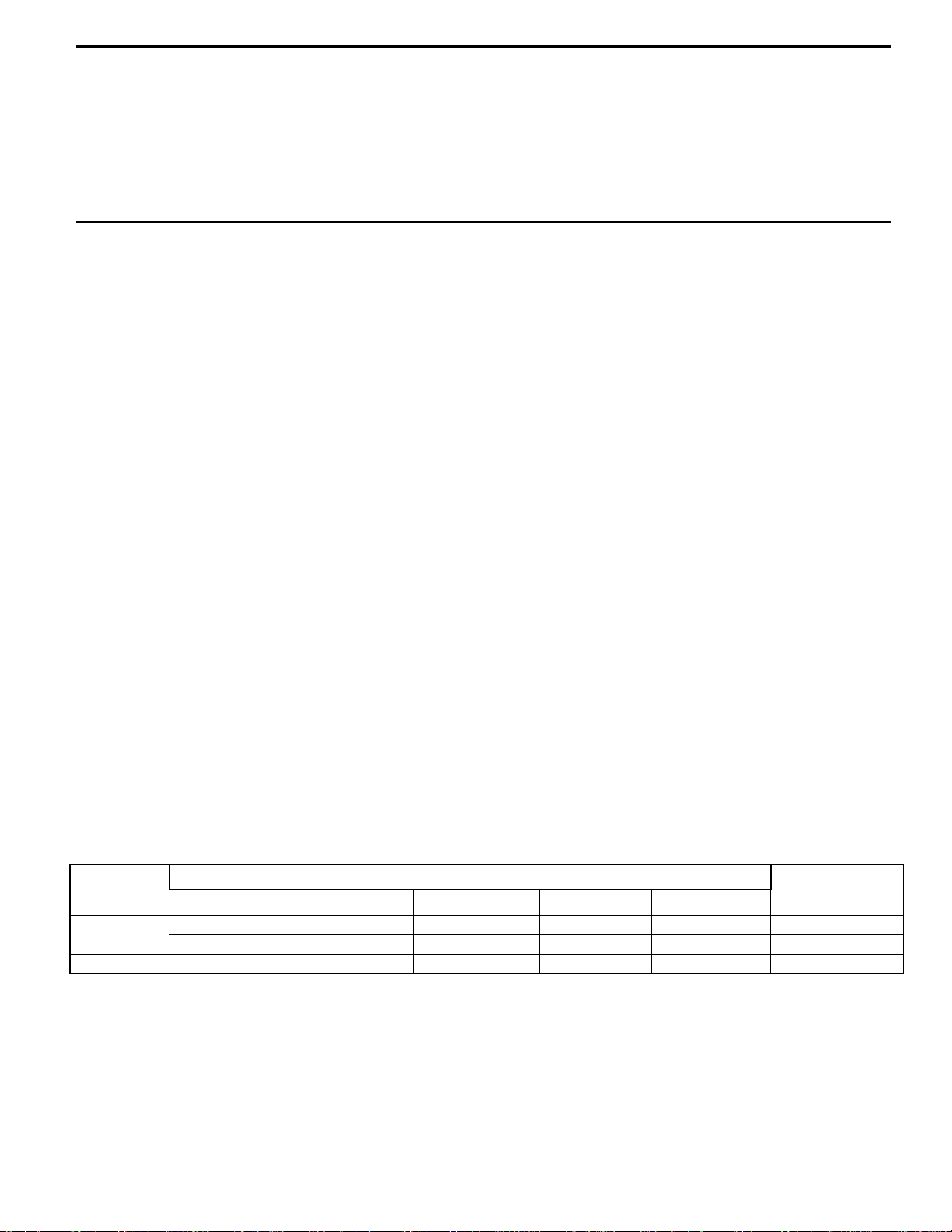
ORDERING INFORMATION
PUT PACKAGE TYPE TEMP.
OUT
VOLTAGE
FIXED AMS3107CN-X AMS3107CL-X AMS3107CD-X AMS3107C-X AMS3107CS-X -40ºC to +85 ºC
AMS3107N-X AMS3107L-X AMS3107D-X AMS3107-X AMS3107S-X -40ºC to +85 ºC
ADJ. AMS3107S -40ºC to +85 ºC
X = 2.0V, 2.5V, 3.0V, 3.3V, 3.5V, 4.0V, 5.0V.
3L TO-92 SOT-89 TO-252 SOT-223 SO-8
RANGE
updated April 24, 2009
http://www.BDTIC.com/AMS
AMS3107
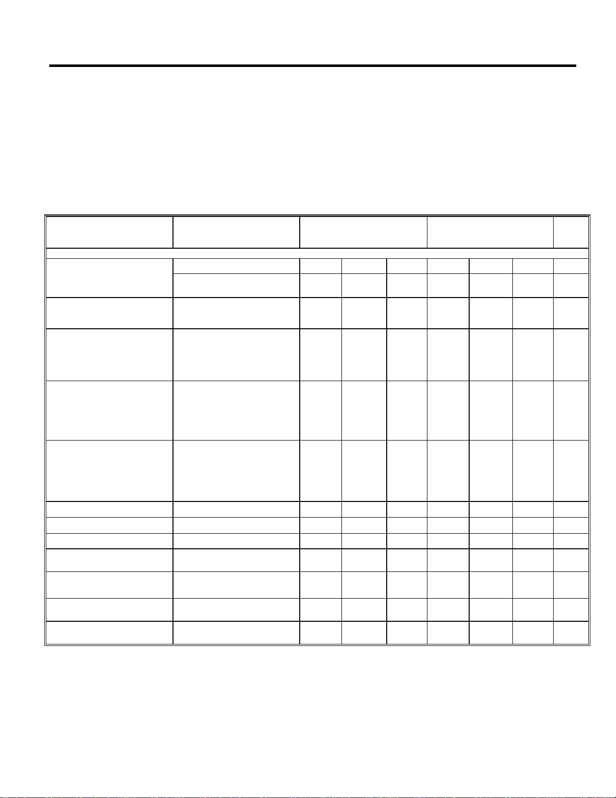
ABSOLUTE MAXIMUM RATINGS (Note 1)
Input Voltage Maximum Junction Temperature
Operating 25V Storage Temperature
-65°C to +150°C
Overvoltage Protection 26V to 40V Lead Temperature (Soldering 25 sec)
Internal Power Dissipation (Note 4) Internally Limited ESD 2000V
ELECTRICAL CHARACTERISTICS
Electrical Characteristics at V
PARAMETER
Fixed Output Voltage Versions
Output Voltage Tolerance -1.0 +1.0 -3.0 +3.0 %
=6.3V, IO =5mA, TJ=25°C, C2 = 22µF unless otherwise specified.
N
I
CONDITIONS
6.3V ≤VIN ≤25V, IO=100 mA
AMS3107C-X
Min. Typ. Max.
- 3.0
+ 3.0
AMS3107-X
Min. Typ. Max.
±±±± 5.0
+125°C
265°C
Units
%
Line Regulation
Load Regulation
Dropout Voltage
Quiescent Current
Output Noise Voltage
Output Bypass Capacitor
Ripple Rejection fO =120Hz 55 80 80 dB
Maximum Operational Input
Voltage
Maximum Line Transient
Reverse Polarity Input Voltage,
D/C
Reverse Polarity Input Voltage,
Transient
6V ≤VIN ≤ 15V
15V ≤VIN ≤ 25V
5mA ≤I
5mA ≤10 ≤ 200 mA
5mA ≤10 ≤ 350 mA
5mA ≤10 ≤ 500 mA
I
O
I
O
I
O
I
O
I
O
I
O
I
O
I
O
10Hz-100kHz, C
ESR=0.1 to 10Ω
25 28 25 28 V
RL = 500Ω, VO ≤ 5.5V
T = 1ms, τ ≤100ms
RL = 500Ω, T = 1ms, τ ≤100ms
≤ 100 mA
O
= 100 mA
= 200 mA
= 350 mA
= 500 mA
≤ 10 mA,
= 100 mA
≤ 200 mA
= 350 mA
= 100µF
OUT
5
50 50
10 10
35 40 35 40 V
-35 -40 -35 -40 V
-35 -40 -35 -40 V
3
5
10
15
20
150
300
400
550
0.18
2
5
12
10
10
10
15
20
30
200
400
450
700
0.25
2.5
8
5
5
5
15
20
20
0.2
250
400
450
550
2
5
12
10
15
15
20
25
30
300
500
550
700
0.3
3
8
mV
mV
mV
mV
mV
mV
mV
mV
mV
mV
mA
mA
mA
mA
µV rms
µF
updated April 24, 2009
http://www.BDTIC.com/AMS
AMS3107
ELECTRICAL CHARACTERISTICS
Electrical Characteristics at V
PARAMETER
Adjustable Version
Reference Voltage
Output Voltage Range 2 24 V
Line Regulation
Load Regulation
Dropout Voltage
Quiescent Current
Output Noise Voltage 10Hz-100kHz 100
Output Bypass Capacitor
Long Term Stability T =1000hr 0.4 %/1000hr
Ripple Rejection fO = 120Hz 0.02 dB
Maximum Operational Input
Voltage
Maximum Line Transient
Reverse Polarity Input Voltage,
D/C
Reverse Polarity Input Voltage,
Transient
On/Off Threshold Voltage
On
Off
On/Off Threshold Current V
Note 1: Absolute Maximum Ratings are limits beyond which damage to the device may occur. For guaranteed performance limits and associated test conditions,
see the Electrical Characteristics tables.
Note 2: To ensure constant junction temperature, low duty cycle pulse testing is used.
Note 3: Limits appearing in boldface type apply over the entire junction temperature range for operation. Limits appearing in normal type apply for TA = TJ =
25°C.
Note 4: The maximum allowable power dissipation is a function of the maximum junction temperature TJ(MAX), the junction-to ambient thermal resistance θ
and the ambient temperature TA. The maximum allowable power dissipation at any ambient temperature is calculated using:
Where the value of the junction-to-ambient thermal resistance are as follows: 195°C/W for TO-92 (N), 160°C/W for the SO-8 (S), 110°C/W for SOT-89 (L),
90°C/W for SOT-223 and 80°C/W for TO-252.
P(MAX)θ=
=6V, V
IN
1.210 1.235 1.26 V
IO ≤ 100 mA, -40°C ≤T
R1=27k, Measured from V
6V ≤VIN ≤ 25V
5mA ≤I
5mA ≤10 ≤ 200 mA
5mA ≤10 ≤ 350 mA
5mA ≤10 ≤ 500 mA
I
= 100 mA
O
I
= 200 mA
O
I
= 350 mA
O
I
= 500 mA
O
I
= 0 mA,
O
I
= 100 mA
O
I
= 200 mA
O
I
= 350 mA
O
ESR=0.1 to 10Ω
IO = 10mA, Reference Voltage ≤ 1.5V
T = 1ms, τ ≤100ms
RL = 500Ω, VO ≥ -0.3V
RL = 500Ω, T = 1ms, τ ≤100ms
VO = 3V
OFF
=3V IO =5mA, TJ=25°C, R1 =27k, C2 = 2µF unless otherwise specified.
OUT
CONDITIONS
(Note 2)
≤ 125°C,
J
to Adj. Pin
OUT
≤ 100 mA
O
= 2.4V 35 60
AJ
T-(MAX)T
A-J
Min.
1.20 1.235 1.270
.02 1.5 mV/V
0.3
0.18
10
21 22 V
35 40 V
-35 -40 V
-35 -40 V
2.5
AMS3107
Typ.
0.5
1.0
1.0
50
300
500
500
2.0
5.0
12
1.8
2.0
Max.
0.5
1
1.5
2.0
200
400
600
700
0.3
2.5
8.0
1.5
Units
V
%
%
%
%
mV
mV
mV
mV
mA
mA
mA
mA
µV
rms
µF
V
V
µA
/V
J-A
updated April 24, 2009

http://www.BDTIC.com/AMS
PIN CONNECTIONS
TO-92
Plastic Package (N)
OUTPUT
INPUT
SOT-89
(L)
AMS3107
SOT-223
GND
1 2 3
Bottom View Top View Top View
TAB IS
GND
TO-252
(D)
3
2
1
OUTPUT
INPUT
OUTPUT
GROUND12
GROUND GROUND
ADJ/ N/C
8L SOIC
SO-Package (S)
3
4
Top View Top View
TYPICAL PERFORMANCE CHARACTERISTICS
OUTPUTGNDINPUT
8
7
6
5
INPUT
GROUND
ON/OFF
1 2 3
OUTPUTGNDINPUT
Dropout Voltage
0.6
0.5
0.4
0.3
0.2
0.1
INPUT OUTPUT DIFFERENTIAL (V)
0
0 40
JUNCTION TEMPERATURE (° C)
IO = 350mA
IO = 200mA
IO = 150mA
IO = 100mA
80
updated April 24, 2009
120
Dropout Voltage
0.6
0.5
0.4
0.3
0.2
0.1
INPUT OUTPUT DIFFERENTIAL (V)
0
0 300
OUTPUT CURRENT (mA)
400 500200100
600
Low Voltage Behavior
OUTPUT VOLTAGE (V)
6.0
5.0
4.0
3.0
2.0
AMS3107-3.3
IO = 500mA
0
2.0 3.0 4.0 5.0 6.0
INPUT VOLTAGE (V)

http://www.BDTIC.com/AMS
TYPICAL PERFORMANCE CHARACTERISTICS (Continued)
AMS3107
Low Voltage Behavior
6.0
5.0
4.0
3.0
2.0
OUTPUT VOLTAGE (V)
0
2.0 3.0 4.0 5.0 6.0
Output Impedance
10
)
Ω
OUTPUT IMPEDANCE (
1
0.1
0.01
1 100
IO = 10mA
AMS3107-5.0
IO = 500mA
INPUT VOLTAGE (V)
1k10 100k
FREQUENCY (Hz)
10k
1M
Output at Voltage Extremes
6
AMS3107-3.3
RL=500m
5
4
3
2
1
OUTPUT VOLTAGE (V)
0
-1
-20 -10 0 10 20 30 40 50 60
Peak Output Current
1200
1000
800
600
400
200
OUTPUT CURRENT (mA)
0
0 10
Ω
INPUT VOLTAGE (V)
TJ= 25°C
20
INPUT VOLTAGE (V)
30
Output at Voltage Extremes
6
AMS3107-5.0
RL=500m
5
4
3
2
1
OUTPUT VOLTAGE (V)
0
-1
-20 -10 0 10 20 30 40 50 60
85
80
75
70
65
60
55
RIPPLE REJECTION (dB)
50
45
1 10 100 1k 10k 100k 1M
Ω
INPUT VOLTAGE (V)
Ripple Rejection
C2 = 100µF
ALUM
IO= 10mA
FREQUENCY (Hz)
C2 = 22µF
TANTALUM
Quiescent Current
17.5
IO= 10mA
15
A)
µ
12.5
10
7.5
5.0
2.5
0
QUIESCENT CURRENT (
-2.5
0 1 2 4 5 6 7 8 10
3 9
INPUT VOLTAGE (V)
updated April 24, 2009
QUIESCENT CURRENT (mA)
10
8
6
4
2
0
0 100
Quiescent Current
VIN = 6V
200
50
150
OUTPUT CURRENT (mA)
250
300
350
Quiescent Current
25
20
15
10
~
~
3
2
1
QUIESCENT CURRENT (mA)
0
-40 40 80 120
0
TEMPERATURE (° C)
IO = 200mA
IO = 100mA
IO = 50mA
IO = 0mA
~
~

http://www.BDTIC.com/AMS
TYPICAL PERFORMANCE CHARACTERISTICS (Continued)
AMS3107
Operation During Load Dump
70
60
50
40
INPUT
OUTPUT
30
20
VOLTAGE (V)
10
0
~
~
5
4
3
2
1
VOLTAGE (V)
0
-100 0
100
TIME (ms)
τ =150
ms
~
CO= 100µF
RL= 500
Ω
200 300 400 500
~
APPLICATION NOTES
Definition of Terms
Dropout Voltage: The input-output voltage differential at which
the circuit stops to regulate against further reduction in input
voltage. Measured when the output voltage has dropped 100mV
from the nominal voltage obtained at 1V input, dropout voltage is
dependent upon load current and junction temperature.
Input Voltage: The DC voltage applied to the input terminal with
respect to ground. Input-Output Differential: The voltage
difference between the unregulated input voltage and the regulated
output voltage for which the regulator will regulate.
Line Regulation: The change in output voltage for a change in
input voltage. The line regulation is measured under conditions
the
of low dissipation or by using low duty cycle pulse testing such
that the average chip temperature is not significantly affected.
Load Regulation: The change in output voltage for a change in
load current at constant chip temperature.
Long term stability: Output voltage stability under accelerated
life-test conditions after 1000 hours with maximum rated voltage
and junction temperature.
Output Noise Voltage: The rms AC voltage at the output, with
constant load and no input ripple, measured over a specified
frequency range.
Quiescent Current: That part of the positive input current that
does not contribute to the positive load current. The regulator
ground lead current.
Ripple Rejection: The ratio of the peak-to –peak input ripple
voltage to the peak-to-peak output ripple voltage at specified
frequency.
Temperature Stability of V
voltage for a thermal variation from room temperature to either
temperature extreme.
External capacitor
The AMS3107 series require an output capacitor of 10µF or
greater to ensure device stability. Without the capacitor the device
may oscillate.
: The percentage change in output
O
Reference Voltage
1.30
AMS3107 ADJUSTABLE
1.28
1.26
1.24
1.22
1.20
1.18
1.16
1.14
REFERENCE VOLTAGE (V)
1.12
1.10
3 6 9 12 15 18 21 240
OUTPUT VOLTAGE (V)
Most type of tantalum or electrolytic capacitor can be used in the
applications. A critical characteristic of the capacitors is an ESR
value of 5Ω or less and a resonant frequency above 500kHz. The
value of this capacitor can be increased without limits.
For higher loads, the value of the capacitor should be increased,
specialy when the output voltage is set for 2.5V or less. The
AMS3107 lowest fixed output voltage value is 2.0V.
Typical application circuit (adjustable output)
V
IN
100k
OFF
10µ
F
ON/OFF
ON
AMS3107
ADJUSTABLE
GND
Minimum Load
In circuits using the fixed output voltage versions, minimum load
is not required. For circuits using the adjustable device, the value
of R1 and R2 should be chosen such, that a current of
approximately 40µA flows through the network. The reference
voltage (1.235V) is measured between the adjust pin and V
The output voltage can be set by the two resistors R1 and R2
using the following equation:
+
R2R1
=
VV REFO
R1
The value of R1 is recommended to be between 25kΩ to 30 kΩ,
and the value of R2 will set the output voltage.
OUT
ADJ
R
28k
R
1
+
2
C1
22µF
V
OUT
.
OUT
updated April 24, 2009

http://www.BDTIC.com/AMS
PACKAGE DIMENSIONS inches (millimeters) unless otherwise noted.
3L TO-92 PLASTIC PACKAGE (N)
0.060±0.005
(1.524±0.127)
DIA
0.180±0.005
(4.572±0.127)
0.180±0.005
(4.572±0.127)
0.90
(2.286)
NOM
0.060±0.010
(1.524±0.254)
AMS3107
0.140±0.010
(3.556±0.127)
10°
NOM
N (TO-92 ) AMS DRW# 042391
0.500
(12.70)
MIN
0.050±0.005
(1.270±0.127)
UNCONTROLLED
0.050
(1.270)
LEAD DIMENSIONS
MAX
0.016±0.003
(0.406±0.076)
5° NOM
0.015±0.002
(0.381±0.051)
8 LEAD SOIC PLASTIC PACKAGE (S)
0.189-0.197*
(4.801-5.004)
8 7 6 5
0.228-0.244
(5.791-6.197)
0.150-0.157**
(3.810-3.988)
1 2 3 4
0.053-0.069
(1.346-1.752)
0.014-0.019
(0.355-0.483)
*DIMENSION DOES NOT INCLUDE MOLD FLASH. MOLD FLASH
SHALL NOT EXCEED 0.006" (0.152mm) PER SIDE
**DIMENSION DOES NOT INCLUDE INT ERLEAD FLASH. INTERLEAD
FLASH SHALL NOT EXCEED 0.010" (0.254mm) PER SIDE
updated April 24, 2009
0.050
(1.270)
TYP
0.004-0.010
(0.101-0.254)
0.008-0.010
(0.203-0.254)
0.010-0.020
(0.254-0.508)
0.016-0.050
(0.406-1.270)
x 45°
0°-8° TYP
S (SO-8 ) AMS DRW# 042293

http://www.BDTIC.com/AMS
PACKAGE DIMENSIONS inches (millimeters) unless otherwise noted (Continued).
SOT-89 PLASTIC PACKAGE (L)
0.173-0.181
0.155-0.167
(3.94-4.25)
0.090-0.102
(2.29-2.60)
(4.40-4.60)
0.064-0.072
(1.62-1.83)
0.035-0.047
(0.89-1.20)
0.055-0.063
(1.40-1.60)
0.084-0.090
(2.13-2.29)
AMS3107
0.014-0.017
(0.35-0.44)
0.264-0.287
(6.71-7.29)
0.130-0.146
(3.30-3.71)
0.059
(1.50)
BSC
0.090
(2.29)
NOM
0.014-0.019
(0.36-0.48)
0.118
(3.00)
BSC
0.017-0.022
(0.44-0.56)
3 LEAD SOT-223 PLASTIC PACKAGE
0.248-0.264
(6.30-6.71)
0.116-0.124
(2.95-3.15)
0.033-0.041
(0.84-1.04)
L (SOT-89 ) AMS DRW# 042392
0.071
(1.80)
MAX
updated April 24, 2009
0.025-0.033
(0.64-0.84)
0.181
(4.60)
NOM
0.012
(0.31)
MIN
10°
MAX
10°-16°
0.025-0.033
(0.64-0.84)
0.010-0.014
(0.25-0.36)
10°-16°
(SOT-223 ) AMS DRW# 042292

http://www.BDTIC.com/AMS
PACKAGE DIMENSIONS inches (millimeters) unless otherwise noted (Continued).
TO-252 PLASTIC PACKAGE (D)
0.258-0.262
(0.508-0.762)
0.023-0.027
(0.584-0.685)
0.020-0.030
0.175-0.180
(4.191-4.445)
(6.553-6.654)
0.208-0.212
(5.283-5.384)
0.020-0.030
(0.508-0.762)
0.033-0.037
(0.838-0.939)
45.0°
0.057-0.067
(0.144-0.170)
DIA
0.085-0.095
(2.159-2.413)
7.0°
0.030-0.034
(0.762-0.863)
0.038-0.042
(0.965-1.066)
0.235-0.245
(5.969-6.223)
AMS3107
0.025
(0.635)
TYP
0.088-0.092
(2.235-2.336)
0.099-0.103
(2.514-2.615)
0.030
(0.762)
TYP
0.038
(0.965)
TYP
0.018-0.022
(0.451-0.558)
0.038-0.042
(0.965-1.066)
0.024±0.002
(0.610±0.0508)
D (D3) AMS DRW# 042891
updated April 24, 2009
 Loading...