

http://www.BDTIC.com/AMS
Advanced AMS2942
Monolithic HIGH VOLTAGE LOW DROPOUT REGULATOR
Systems
RoHS compliant
FEATURES APPLICATIONS
• Adjustable from 1.23V to 42V • Telephone Systems
• High Accuracy Output Voltage • High Voltage Power Supply
• Extremely Low Quiescent Current • Cordless Telephones
• Low Dropout Voltage • Laboratory Instrumentation
• Tight Load and Line Regulation • Radio Control Systems
• Low Temperature Coefficient • Automotive Electronics
• Current and Thermal Protection • Avionics
• Unregulated DC Positive Transients 60V
• Error Flag Warning of Voltage Output Dropout
• Logic Controlled Electronic Shutdown
GENERAL DESCRIPTION
The AMS2942 are micropower voltage regulators ideally suited for use with high voltage powered systems. This device
feature very low quiescent current (typ.130µA), and very low dropout voltage (typ.45mV at light loads and 380mV at
100mA). The quiescent current increases only slightly in dropout. The AMS2942 has positive transient protection up to 60V
and can survive unregulated input transient up to 20V below ground.
AMS2942 is designed with a tight initial voltage reference tolerance, excellent load and line regulation (typ. 0.05%), and a
very low output voltage temperature coefficient, making these devices useful as a low-power voltage regulator in telephone
applications, using the telephone line as a power source.
The AMS2942 is available in a special 8-pin plastic SOIC in which pin 2 and 3 are fused together with the package paddle
serving also as heat sink. An error flag output warns of a low output voltage, often due to failing voltage on input line. A
logic-compatible shutdown input is available, which enables the regulator to be switched on and off. The output voltage can be
programmed from 1.23V to 42V with an external pair of resistors.
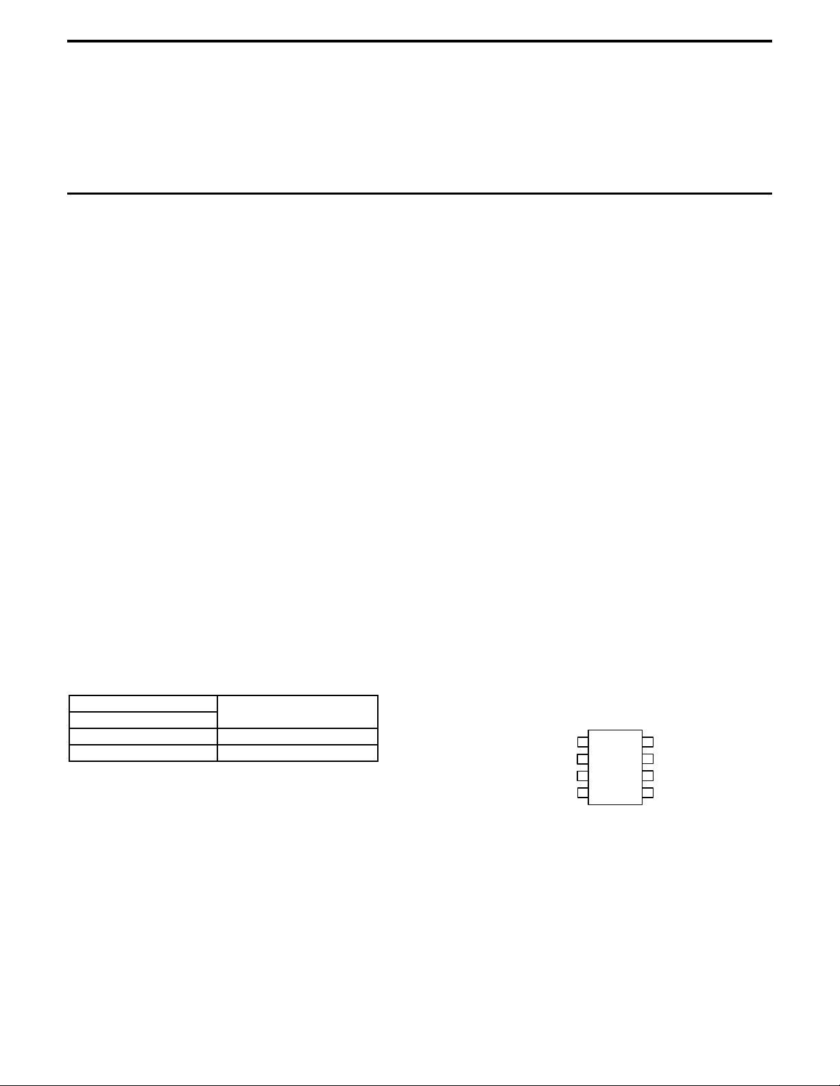
ORDERING INFORMATION PIN CONNECTION
PACKAGE TYPE OPERATING
8 LEAD SOIC
AMS2942AS IND
AMS2942BS IND
TEMP. RANGE
8L SOIC
1
OUTPUT INPUT
ON/OFF
2
3
4
Top View
GROUND
GROUND
8
7
FEEDBACK
6 N/C
5
ERROR
Advanced Monolithic Systems, Inc.
AMS2942
http://www.BDTIC.com/AMS
ABSOLUTE MAXIMUM RATINGS (Note 1)
Input Supply Voltage -0.3 to +50V ESD 2000V
Power Dissipation Internally Limited
Junction Temperature
Storage Temperature
Soldering (25 Sec.)
-65°C to +150°C
+150°C
265°C
(T
OPERATING RATINGS (Note 1)
Max. Input Supply Voltage 45V
Junction Temperature Range
) (Note 8)
J
-40°C to +125°C
ELECTRICAL CHARACTERISTICS at V
Parameter Conditions
Reference Voltage 1.22 1.235 1.25 1.21 1.235 1.26 V
Reference Voltage Over Temperature (Note 7)
Output Voltage
Temperature Coefficient
Line Regulation (Note 12)
Load Regulation (Note 12)
Dropout Voltage
(Note 5)
Ground Current
Current Limit V
Thermal Regulation (Note 11) 0.05 0.2 0.05 0.2 %/W
Output Noise,
10Hz to 100KHz
Feedback Pin Bias Current 40 80 40 80 nA
Reference Voltage Temperature
Coefficient
Feedback Pin Bias Current
Temperature Coefficient
Error Comparator
Output Leakage Current V
Output Low Voltage
Upper Threshold Voltage (Note 6) 40 60 40 60 mV
Lower Threshold Voltage (Note 6) 75 95 75 95 mV
Hysteresis (Note 6) 15 15 mV
Shutdown Input
Input logic Voltage
Shutdown Pin Input Current
(Note 3)
Regulator Output Current in
Shutdown (Note 3)
(Note 10) (Note 4)
6V ≤ V
100 µA ≤I
I
= 100µ A
L
I
= 100 mA
L
= 100 µA
I
L
I
= 100 mA
L
OUT
= 1µF
C
L
C
= 200 µF
L
C
= 13.3 µF
L
(Bypass = 0.01 µF pins 7 to 1)
( Note 10) 20 50 ppm/° C
OH
V
IN
Low (Regulator ON)
High (Regulator OFF)
V
= 2.5V
S
V
= 42V
S
(Note 9) 15 50 15 50
(Note 2)
≤ 45V (Note 13)
IN
≤ 100 mA
L
= 0 160 200 160 200 mA
= 42V
= 4.5V, IOL = 400µA
=V
+1V, TA=25°C, unless otherwise specified.
OUT
S
AMS2942A
Min. Typ. Max.
1.19 1.27 1.185 1.285
0.05 0.2 0.1 0.4 %
0.05 0.2 0.1 0.4 %
150 250 150 250 mV
2.5
20 50
50
380
120
8
430
160
100
0.1 0.1 nA/°C
0.05 2 0.05 2
1.3
30
600
AMS2942B
Min. Typ. Max.
80
450
180
12
430
0.7
60
850
120 8 180
2.5
30
50
380
160
100
1.3
600
ppm/°C
80
450
12
0.7
60
850
Units
V
mV
mV
µA
mA
µV rms
µV rms
µV rms
µA
V
V
µA
µA
µA
Advanced Monolithic Systems, Inc.
http://www.BDTIC.com/AMS
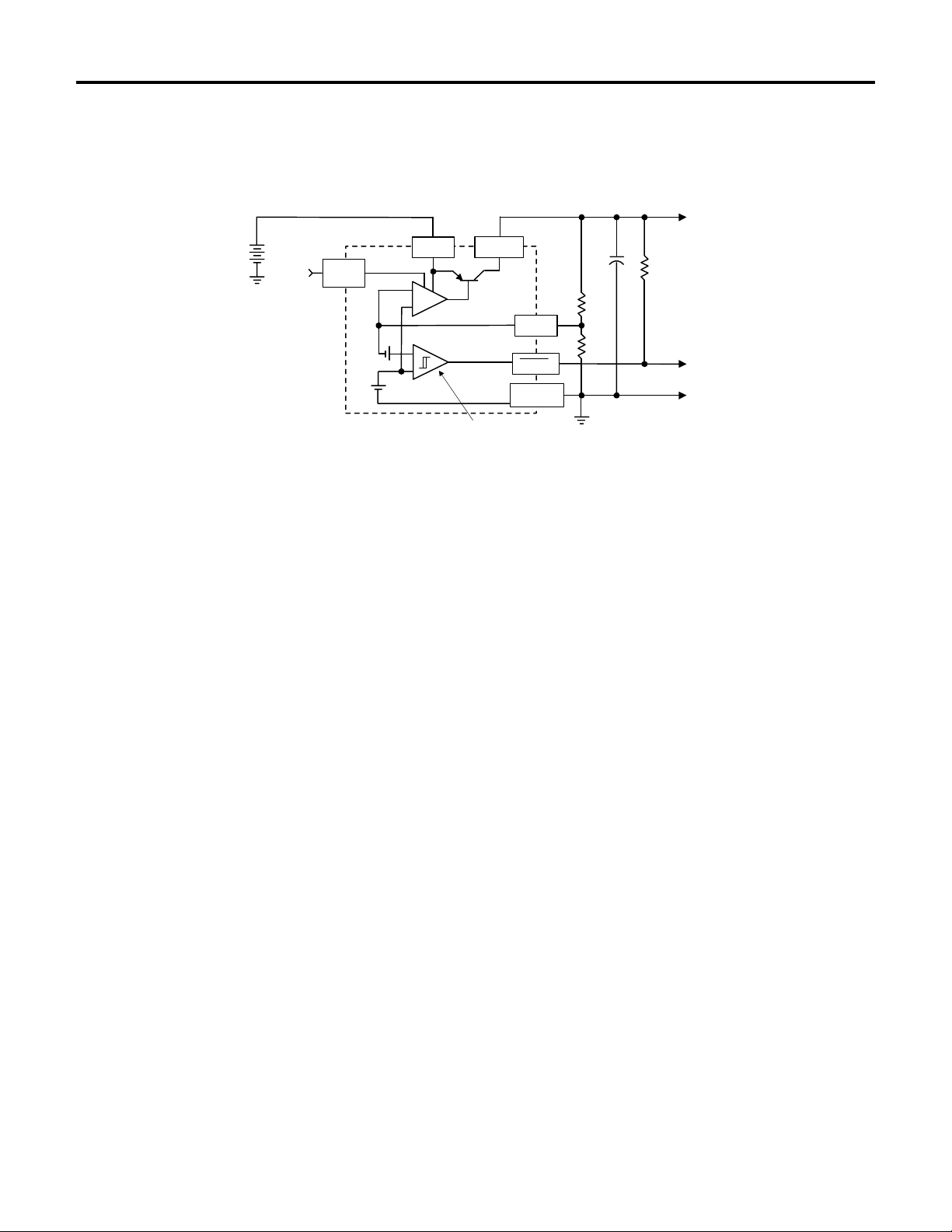
BLOCK DIAGRAM AND TYPICAL APPLICATIONS
AMS2942
AMS2942
39V to 45V UNREGULATED DC
+
FROM
CMOS
OR TTL
SHUTDOWN
ERROR DETECTION COMPARATOR
50mV
+
INPUT OUTPUT
+
ERROR
AMPLIFIER
+
+
-
1.23V
REFERENCE
FEEDBACK
ERROR
GROUND
10µF
298k
10k
+
330k
Ω
Ω
V
Ω
TO CMOS
OR TTL
= 38V
O
Note 1: Absolute Maximum Ratings are limits beyond which damage to the device may occur. Operating Ratings are conditions under which operation of the
device is guaranteed. Operating Ratings do not imply guaranteed performance limits. For guaranteed performance limits and associated test conditions, see the
Electrical Characteristics tables.
Note 2: Unless otherwise specified all limits guaranteed for V
IN
= ( V
entire junction temperature range for operation. Limits appearing in normal type apply for T
+1)V, IL = 100 µA and CL = 1 µF. Limits appearing in boldface type apply over the
ONOM
= TJ = 25°C, V
A
SHUTDOWN
≤ 0.8V.
Note 3: Guaranteed and 100% production tested.
Note 4: Guaranteed but not 100% production tested. These limits are not used to calculate outgoing AQL levels.
Note 5: Dropout voltage is defined as the input to output differential at which the output voltage drops 100 mV below its nominal value measured at 1V
differential. At very low values of programmed output voltage, the minimum input supply voltage of 2V ( 2.3V over temperature) must be taken into account.
Note 6: Comparator thresholds are expressed in terms of a voltage differential at the feedback terminal below the nominal reference voltage measured at
= ( V
V
IN
+1)V. To express these thresholds in terms of output voltage change, multiply by the error amplifier gain = Vout/Vref = (R1 + R2)/R2. For
ONOM
example, at a programmed output voltage of 5V, the error output is guaranteed to go low when the output drops by 95 mV x 5V/1.235 = 384 mV. Thresholds
as V
remain constant as a percent of V
Note 7: V
≤ (Vin - 1V), 2.3 ≤Vin≤42V, 100µA≤IL≤ 100 mA, TJ ≤ T
ref ≤Vout
is varied, with the dropout warning occurring at typically 5% below nominal, 7.5% guaranteed.
out
out
JMAX
.
Note 8: The junction-to-ambient thermal resistance is 120°C/W for the molded plastic SO-8 (S), when the package is soldered directly to the PCB.
Note 9: V
≥ 2.5V, VIN ≤ 42V, V
SHUTDOWN
OUT
=0.
Note 10: Output or reference voltage temperature coefficients defined as the worst case voltage change divided by the total temperature range.
Note 11: Thermal regulation is defined as the change in output voltage at a time T after a change in power dissipation is applied, excluding load or line
regulation effects. Specifications are for a 50mA load pulse at V
=42V (1.25W pulse) for T =10 ms.
IN
Note 12: Regulation is measured at constant junction temperature, using pulse testing with a low duty cycle. Changes in output voltage due to heating effects
are covered under the specification for thermal regulation.
Note 13: Line regulation is tested at 150°C for I
performance characteristics for line regulation versus temperature and load current.
= 1 mA. For IL = 100 µA and TJ = 125°C, line regulation is guaranteed by design to 0.2%. See typical
L
Advanced Monolithic Systems, Inc.

http://www.BDTIC.com/AMS
TYPICAL PERFORMANCE CHARACTERISTICS
Quiescent Current
10
1
0.1
GROUND CURRENT (mA)
0.01
0.1 1 10 100
LOAD CURRENT (mA)
Quiescent Current
160
140
A)
µ
120
100
80
60
40
20
QUIESCENT CURRENT (
0
012345678
INPUT VOLTAGE (V)
IL= 1 mA
IL= 0
AMS2942
Quiescent Current
9
8
QUIESCENT CURRENT (mA)
7
-75
-50 -25
0 25 50 75 100 12510150
TEMPERATURE (° C)
VIN= V
OUT
IL= 100mA
+1V
Short Circuit Current
170
160
150
140
130
120
110
SHORT CIRCUIT CURRENT ( mA)
100
-50 -25
-75 0 25 50 75 100 125
2.2
2.1
2.0
1.9
1.8
1.7
1.6
MINIMUM OPERATING VOLTAGE (V)
-75 0
TEMPERATURE (° C)
Minimum Operating Voltage
-50 -25
25 50 75
TEMPERATURE (° C)
100
125
150
150
Dropout Voltage
600
500
400
300
~
~
100
50
DROPOUT VOLTAGE (mV)
0
-50 -25
-75 0 25 50 75 100 125
20
10
0
-10
-20
BIAS CURRENT (nA)
-30
-75 0 25 50 75 100
TEMPERATURE (° C)
Feedback Bias Current
-50 -25
TEMPERATURE (° C)
IL= 100mA
IL= 100µA
125
150
150
Dropout Voltage
500
400
300
200
TJ = 25°C
100
DROPOUT VOLTAGE (mV)
0
100µA 1mA 10mA 100mA
50
A)
0
µ
-50
-100
-150
-200
FEEDBACK CURRENT (
-250
-2.0 -1.5 -1.0 -0.5
OUTPUT CURRENT
Feedback Pin Current
PIN 7 DRVEN BY EXTERNAL
SOURCE (REGULATOR RUN
OPEN LOOP)
TA = 125°C
TA = 25°C
TA = -55°C
FEEDBACK VOLTAGE (V)
0 0.5
1.0
Advanced Monolithic Systems, Inc.

http://www.BDTIC.com/AMS
TYPICAL PERFORMANCE CHARACTERISTICS (Continued)
OUTPUT VOLTAGE
LOAD
Load Transient Response
250
200
150
100
50
0
CHANGE (mV)
-50
-100
~
~
100
mA
100
µ
A
CURRENT
01 23 4 5
TIME (ms)
CL= 1 µF
OUTPUT VOLTAGE
LOAD
Load Transient Response
80
60
40
20
0
-20
CHANGE (mV)
-40
-60
~
~
100
mA
100
µ
A
CURRENT
04 8121620
TIME (ms)
CL= 10 µF
7
6
5
4
3
OUTPUT
VOLTAGE (V)
2
1
0
2
0
-2
VOLTAGE (V)
SHUTDOWN PIN
AMS2942
Enable Transient
CL= 1 µF
CL= 10 µF
~
~
0 100 200 300 400 500 600 700-100
TIME (
IL= 10 mA
V
= 8V
IN
µ
s)
Output Impedance
10
5
)
Ω
2
1
IO= 100µA
IO= 1 mA
0.5
0.2
0.1
0.05
OUPUT IMPEDANCE (
0.02
0.01
10 100 1K 100K
FREQUENCY (Hz)
Error Comparator Output
9
V
= 5V
OUT
8
7
6
50k RESISTOR TO
EXTERNAL 5V SUPPLY
5
4
3
ERROR OUTPUT (V)
2
1
0
0 345678
50k
RESISTOR
TO V
12
INPUT VOLTAGE (V)
IO= 100mA
V
CL= 1 µF
10K 1M
HYSTERESIS
OUT
OUT
= 5V
Ripple Rejection
90
80
70
60
50
40
CL= 1 µF
RIPPLE REJECTION (dB)
VIN= 6V
30
V
= 5V
OUT
20
10
2
1
10
3
10
FREQUENCY (Hz)
Error Comparator Sink Current
2.5
2.0
1.5
1.0
SINK CURRENT (mA)
0.5
0.0
0.0 0.3 0.4 0.5 0.6 0.7 0.8
0.1 0.2
OUTPUT LOW VOLTAGE (V)
10
IL= 0
4
IL= 100µA
5
10
TA = 125°C
TA = 25°C
TA = -55°C
10
0.9
Ripple Rejection
90
80
70
IL= 1mA
CL= 1 µF
VIN= V
OUT
+1V
60
50
40
RIPPLE REJECTION (dB)
30
6
20
1
10
10
IL= 10mA
5
2
10
4
3
10
10
6
10
FREQUENCY (Hz)
Line Transient Response
100
mV
50
mV
0
CHANGE
mV
OUTPUT VOLTAGE
INPUT
VOLTAGE
-50
8V
6V
4V
~
~
200 400 600
0
CL= 1µF
IL= 1mA
V
OUT
= 5V
800
TIME (µs)
Advanced Monolithic Systems, Inc.

http://www.BDTIC.com/AMS
APPLICATION HINTS
External Capacitors
A 1.0 µF or greater capacitor is required between output and
ground for stability at output voltages of 5V or more. At lower
output voltages, more capacitance is required. Without this
capacitor the part will oscillate. Most types of tantalum or
aluminum electrolytic works fine here; even film types work but
are not recommended for reasons of cost. Many aluminum types
have electrolytes that freeze at about -30°C, so solid tantalums are
recommended for operation below -25°C. The important
parameters of the capacitor are an ESR of about 5 Ω or less and
resonant frequency above 500 kHz parameters in the value of the
capacitor. The value of this capacitor may be increased without
limit.
At lower values of output current, less output capacitance is
required for stability. The capacitor can be reduced to 0.33 µF for
currents below 10 mA or 0.1 µF for currents below 1 mA. At
voltages below 5V the error amplifier operates at lower gains so
that more output capacitance is needed. For the worst-case
situation of a 100mA load at 1.23V output (Output shorted to
Feedback) a 3.3µF (or greater) capacitor should be used.
A 1µF tantalum or aluminum electrolytic capacitor should be
placed between input to ground if there is more than 10 inches of
wire between the input and the AC filter capacitor or if a battery is
used as the input.
Stray capacitance to Feedback terminal can cause instability. This
may especially be a problem when using a higher value of external
resistors to set the output voltage. Adding a 100 pF capacitor
between Output and Feedback and increasing the output capacitor
to at least 3.3 µF will fix this problem.
Error Detection Comparator Output
The comparator produces a logic low output whenever the output
falls out of regulation by more than approximately 5%. This figure
is the comparator’s built-in offset of about 60 mV divided by the
1.235 reference voltage. This trip level remains “5% below
normal” regardless of the programmed output voltage. For
example, the error flag trip level is typically 4.75V for a 5V output
or 11.4V for a 12V output. The out of regulation condition may be
due either to low input voltage, current limiting, or thermal
limiting.
Figure 1 gives a timing diagram depicting the ERROR signal and
the regulator output voltage as the AMS2942 input is ramped up
and down.
Since the dropout voltage is load dependent the input voltage trip
point will vary with the load current. The output voltage trip point
does not vary with load. The error comparator has an opencollector output which requires an external pullup resistor. This
resistor may be returned to the output or some other supply
voltage depending on system requirements. In determining a
value for this resistor, note that the output is rated to sink 400µA.
Suggested values range from 100K to 1MΩ. The resistor is not
required if error flag terminal is unused.
AMS2942
Setting the Output Voltage
The AMS2942 it may be programmed for any output voltage
between its 1.235V reference and its 42V maximum rating. As
seen in Figure 2, an external pair of resistors is required.
The complete equation for the output voltage is:
V
where V
feedback pin bias current, nominally -20 nA. The minimum
recommended load current of 1 µA forces an upper limit of 1.2
MΩ on value of R
condition often found in CMOS in standby) I
typical error in V
temperature by trimming R
100k reduces this error to 0.17%.
Reducing Output Noise
In reference applications it may be an advantageous to reduce the
AC noise present at the output. One method is to reduce the
regulator bandwidth by increasing the size of the output capacitor.
Noise could be reduced fourfold by a bypass capacitor across R
since it reduces the high frequency gain from 4 to unity. Pick
C
or about 0.01 µF. When doing this, the output capacitor must be
increased to 3.3 µF to maintain stability. These changes reduce
the output noise from 430 µV to 100 µV rms for a 100 kHz
bandwidth at 5V output. With the bypass capacitor added, noise
no longer scales with output voltage so that improvements are
more dramatic at higher output voltages.
= V
out
REF
BYPASS
× (1 + R1/ R2)+ IFBR
REF
1
is the nominal 1.235 reference voltage and IFB is the
, if the regulator must work with no load (a
2
which may be eliminated at room
OUT
. For better accuracy, choosing R2 =
1
will produce a 2%
FB
≅ 1 / 2πR1 × 200 Hz
,
1
Advanced Monolithic Systems, Inc.

http://www.BDTIC.com/AMS
APPLICATION HINTS (Continued)
OUTPUT
VOLTAGE
ERROR*
INPUT
VOLTAGE
4.75V
1.3V
5V
FIGURE 1. ERROR Output Timing FIGURE 2. Adjustable Regulator
*When V
and the error flag voltage rises to its pull-up voltage. Using V
as the pull-up voltage (see Figure 2), rather than an external 5V
source, will keep the error flag voltage under 1.2V (typ.) in this
condition. The user may wish to drive down the error flag
voltage using equal value resistors (10 kΩ suggested), to ensure a
low-level logic signal during any fault condition, while still
allowing a valid high logic level during normal operation.
≤1.3V the error flag pin becomes a high impedance,
IN
*See Application Hints.
out
= V
V
out
REF
**Drive with TTL- high to shut down. Ground or leave if shutdown
feature is not used.
Note: Pins 2 and 6 are left open.
PACKAGE DIMENSIONS inches (millimeters) unless otherwise noted.
8 LEAD SOIC PLASTIC PACKAGE (S)
100k
ERROR
OUPUT
**SHUTDOWN
INPUT
× (1 + R1/ R2)
ERROR*
4
SD
+V
+V
AMS2942
GND
3
AMS2942
IN
8
IN
15
V
OUT
R
1
FB
1.23
7
2
V
R
V
2
REF
V
OUT
1.2 30V
+*
.01µ
F
3.3
µ
F
0.189-0.197*
(4.801-5.004)
87 65
0.228-0.244
(5.791-6.197)
12 34
0.053-0.069
(1.346-1.752)
0.014-0.019
(0.355-0.483)
*DIMENSION DOES NOT INCLUDE MOLD FLASH. MOLD FLASH
SHALL NOT EXCEED 0.006" (0.152mm) PER SIDE
**DIMENSION DOES NOT INCLUDE INTERLEAD FLASH. INTERLEAD
FLASH SHALL NOT EXCEED 0.010" (0.254mm) PER SIDE
Advanced Monolithic Systems, Inc.
0.050
(1.270)
TYP
0.150-0.157**
(3.810-3.988)
0.004-0.010
(0.101-0.254)
0.008-0.010
(0.203-0.254)
0.010-0.020
(0.254-0.508)
0.016-0.050
(0.406-1.270)
x 45°
0°-8° TYP
S (SO-8 ) AMS DRW# 042293
 Loading...