

http://www.BDTIC.com/AMS
Advanced AMS2930
Monolithic 150mA LOW DROPOUT VOLTAGE REGULATOR
Systems
RoHS compliant
FEATURES APPLICATIONS
•••• Fixed and Adjustable Versions Available •
•••• Output Current in excess of 150mA •••• Portable Consumer Equipment
•••• Very Low Quiescent Current •••• Cordless Telephones
•••• Reverse Battery Protection •••• Portable (Notebook) Computers
•••• Input-output Differential less than 0.6V •••• Portable Instrumentation
•••• Short Circuit protection •••• Radio Control Systems
•••• Internal Thermal Overload Protection •••• Automotive Electronics
•••• 60V Load Dump Protection
•••• -50V Reverse Transient Protection
•••• Mirror Image Insertion Protection
PRODUCT DESCRIPTION
The AMS2930 series consists of positive fixed and adjustable voltage regulators ideally suited for use in battery-powered
systems. These devices feature very low quiescent current of 1mA or less when supplying 10mA loads. This unique
characteristic and the extremely low input -output differential required for proper regulation (0.2V for output currents of 10mA)
make the AMS2930 ideal to use for standby power systems.
Originally designed for automotive applications, the AMS2930 and all regulated circuitry are protected from input fault
conditions caused by reverse battery installation or two battery jump starts. During line transients, such as load dump (60V)
when the input voltage to the regulator can momentarily exceed the specified maximum operating voltage, the regulator will
automatically shut down to protect both internal circuits and the load. The AMS2930 series also includes internal current
limiting, thermal shutdown, and is able to withstand temporary power-up with mirror-image insertion.
The AMS2930 is offered in the 3-pin TO-92 package, 8-pin plastic SOIC, TO-220 and TO-263 packages.
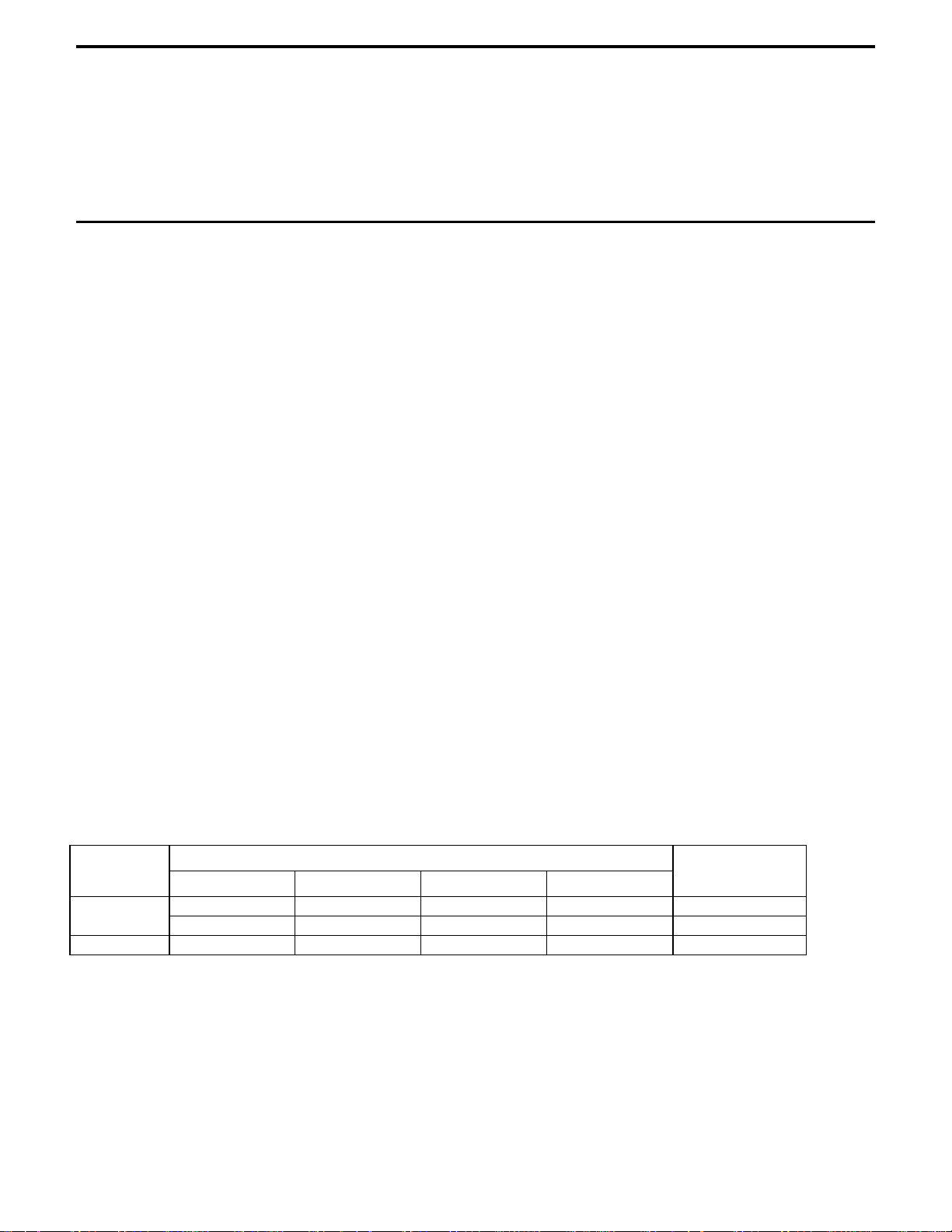
ORDERING INFORMATION
PUT PACKAGE TYPE OPER. TEMP
OUT
VOLTAGE
FIXED* AMS2930AN-X AMS2930AS-X AMS2930AT-X AMS2930AM-X -40ºC to +85ºC
AMS2930N-X AMS2930S-X AMS2930T-X AMS2930M-X -40ºC to +85ºC
ADJ. AMS2930CS -40ºC to +85ºC
X = 2.0V, 2.5V, 3.0V, 3.3V, 3.5V, 4.0V, 5.0V
*For additional available fixed voltages contact factory
TO-92 8 LEAD SOIC TO-220 TO-263
• Battery Powered Systems
•
•
RANGE
updated April 24, 2009
http://www.BDTIC.com/AMS
AMS2930
ABSOLUTE MAXIMUM RATINGS (Note 1)
Overvoltage Protection
OPERATING CONDITIONS (Note 1)
AMS2930A-X, AMS2930C 60V Input voltage range 4V to 22V
AMS2930-X 50V Junction Temperature
+125°C
Maximum Input Voltage 22V Lead Temperature (Sold. 25 sec)
Internal Power Dissipation (Note 4) Internally Limited ESD 2000V
Reverse Voltage (100ms) -12V
Storage Temperature
-65°C to +150°C
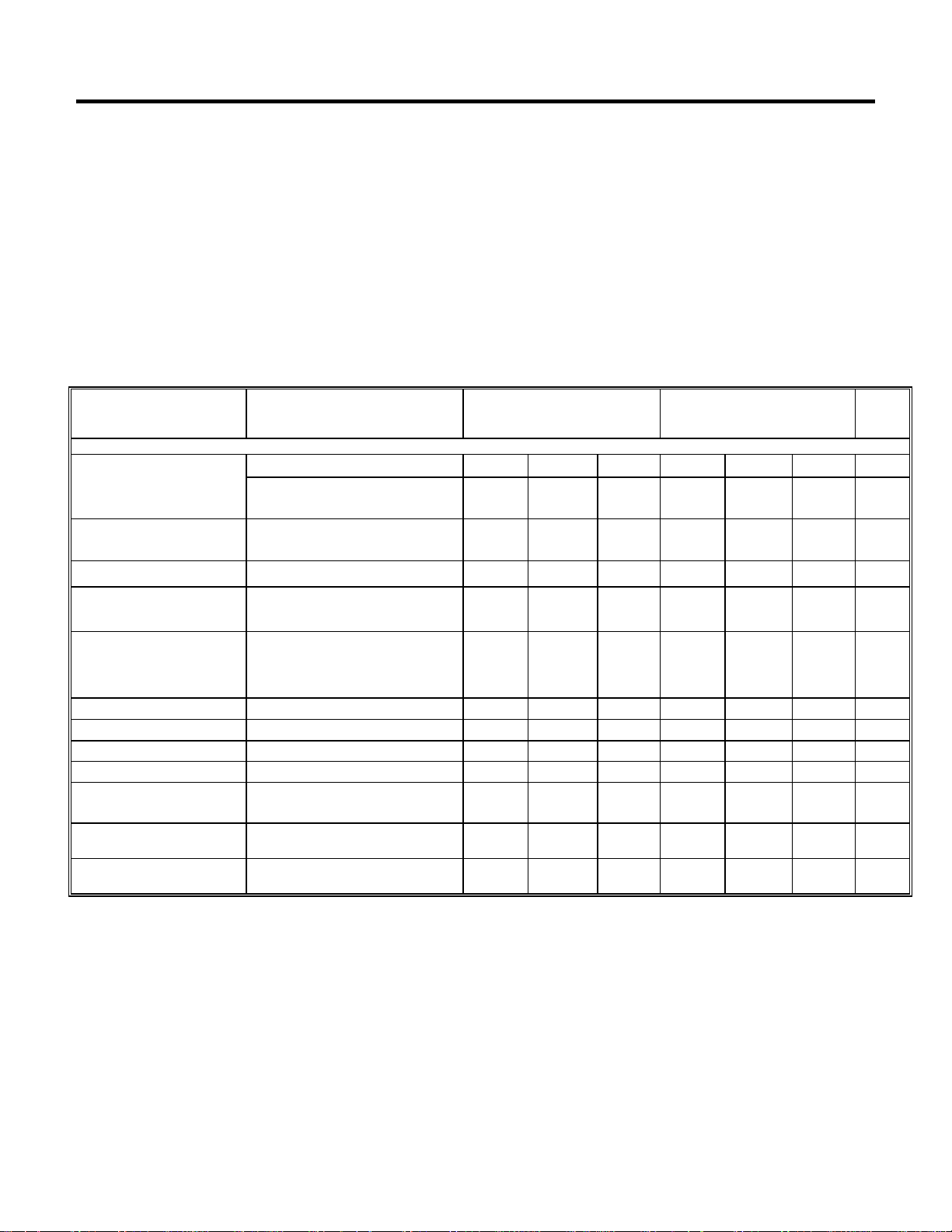
ELECTRICAL CHARACTERISTICS
Electrical Characteristics at V
PARAMETER
Fixed Output Voltage Versions
Output Voltage Tolerance -1.0 +1.0 -3.0 +3.0 %
Line Regulation
Load Regulation
Dropout Voltage
Quiescent Current
Output Noise Voltage
Output Impedance 100mADC and 10mA
Long Term Stability T =1000hr 20 20 mV
Ripple Rejection fO =120Hz
Maximum Line Transient
Reverse Polarity Input Voltage,
D/C
Reverse Polarity Input Voltage,
Transient
=14V, TJ=25°C, C2 = 100µF unless otherwise specified.
N
I
CONDITIONS
6V ≤VIN ≤26V, IO=100 mA
-40°C ≤T
9V ≤VIN ≤ 16V
6V ≤VIN ≤ 26V
5mA ≤I
I
O
I
O
I
O
-40°C ≤T
I
O
10Hz-100kHz, C
RL = 500Ω, VO ≤ 5.5V
T = 1ms, τ ≤100ms
RL = 500Ω, T = 1ms, τ ≤100ms
≤125°C
J
≤ 150 mA
O
= 10 mA
= 150 mA
≤ 10 mA, 6V ≤ VIN ≤ 26V
≤ 125°C
J
= 150 mA, V
= 14V, TJ = 25°C
IN
= 100µA
OUT
,100Hz=10kHz 160 200 160 200
rms
AMS2930A-X
Min. Typ. Max.
- 3.0
14 50 14 50 mV
5
500 500
55
60 70 50 70 V
-15 -30 -15 -30 V
-50 -80 -50 -80 V
2
4
50
300
0.4
15
80 80 dB
+ 3.0
10
30
200
600
1.0
30
AMS2930-X
Min. Typ. Max.
2
0.4
±±±± 5.0
4
50
300
15
%
10
30
200
600
1.0
265°C
Units
µV rms
mV
mV
mV
mV
mA
mA
mΩ
updated April 24, 2009
http://www.BDTIC.com/AMS
AMS2930
Electrical Characteristics
Electrical Characteristics at VIN=14V, V
PARAMETER
Adjustable Version
Reference Voltage
Output Voltage Range 3 24 V
Line Regulation
Load Regulation
Dropout Voltage
Quiescent Current
Output Noise Voltage 10Hz-100kHz 100
Output Impedance 100mADC and 10mA
Long Term Stability T =1000hr 0.4 %/1000hr
Ripple Rejection fO = 120Hz 0.02 %/V
Maximum Operating Input
Voltage
Maximum Line Transient
Reverse Polarity Input Voltage,
D/C
Reverse Polarity Input Voltage,
Transient
On/Off Threshold Voltage
On
Off
On/Off Threshold Current 20 50
Note 1: Absolute Maximum Ratings are limits beyond which damage to the device may occur. For guaranteed performance limits and associated test
conditions, see the Electrical Characteristics tables.
Note 2: See Circuit in Typical Applications. To ensure constant junction temperature, low duty cycle pulse testing is used.
Note 3: Limits appearing in boldface type apply over the entire junction temperature range for operation. Limits appearing in normal type apply for
TA = TJ = 25°C.
Note 4: The junction-to-ambient thermal resistance are as follows: 195°C/W for the TO-92 (N) package, 160°C/W for the molded plastic SO-8 (S), 50°C/W
for the TO-220 package and 73°C/W for the TO-263 package. If the TO-220 package is used with a heat sink, θJA is the sum of the package thermal resistance
junction-to-case of 3°C/W and the thermal resistance added by the heat sink and the thermal interface. The thermal resistance of the TO-263 package can be
reduced by increasing the PCB copper area thermally connected to the package: using 0.5 square inches of copper area, ϕ JA is 50°C/W; with 1 square inch of
copper area ϕ JA is 37°C/W; and with 1.6 or more square inches of copper area ϕ JA is 32°C/W.
1.14 1.20 1.26 V
IO ≤ 150 mA, -40°C ≤T
Measured from V
V
+ 0.6V ≤VIN ≤ 26V
OUT
5mA ≤IO ≤ 150 mA
I
≤10 mA
O
I
= 150 mA
O
I
= 10 mA
O
I
= 150 mA
O
During Shutdown RL = 500Ω
IO = 10mA, Reference Voltage ≤ 1.5V
T = 1ms, τ ≤100ms
RL = 500Ω, VO ≥ -0.3V
RL = 500Ω, T = 1ms, τ ≤100ms
VO = 3V
=3V IO =150mA, TJ=25°C, R1 =27k, C2 = 100µF unless otherwise specified.
OUT
CONDITIONS
(Note 2)
≤ 125°C, R1=27k,
J
to Adjust Pin
OUT
,100Hz=10kHz 40
rms
Min.
1.08 1.32
.02 1.5 mV
0.3 1 %
21 22 V
60 70 V
-15 -30 V
-50 -80 V
3.25
AMS2930C
Typ.
0.05
0.3
0.4
15
0.8
2.0
2.2
Max.
0.2
0.6
1
1
1.2
Units
V
V
V
mA
mA
mA
µV
rms
mΩ
V
V
µA
/V
updated April 24, 2009

http://www.BDTIC.com/AMS
PIN CONNECTIONS
FIXED OUTPUT VOLTAGE
TO-92
Plastic Package (N)
OUTPUT
GND
INPUT
GROUND
GROUND GROUND
8L SOIC
SO-Package (S)
1
OUTPUT
2
3
N/C
4
TO-220 (T) TO-263 (M)
8
INPUT
GROUND
7
6
N/C
5
GND
Bottom View
Top View
Front View
ADJUSTABLE OUTPUT VOLTAGE
8L SOIC
SO-Package (S)
1
OUTPUT
2
GROUND
GROUND GROUND
3
ADJ
4
8
INPUT
GROUND
7
6
ON/OFF
5
Top View
TYPICAL APPLICATIONS
AMS2930-X (Fixed Output) AMS
UNREGULATED
INPUT
IN
C1*
0.1µF
AMS2930
GND
I
Q
V
*Required if regulator is located far from power supply filter.
**C2 must be at least 100µF to maintain stability; it can be increased
without bound to maintain regulation during transients and it should be
located as close as possible to the regulator. This capacitor must be rated
over the same operating temperature range like the regulator. The ESR
of this capacitor is critical (see curve) and it should by less than 1Ω over
the expected operating temperature range.
updated April 24, 2009
V
REGULATED
OUTPUT
C2**
100µF
OUT
R
3
51k
OFF
= V
REF
C1*
0.1µF
× ( R1+R2)/R
ON
V
OUT
Note: Using 27k for R1 will automatically compensate for errors in V
due to the input bias current of the Adjust Pin ( approx. 1µA)
AMS2930
OUTPUT
GND
INPUT
2930C (Adjustable Output)
ON/OFF
1
AMS2930
ADJUSTABLE
GND
TAB IS
GND
Top View
V
CC
OUT
R
1
28k
ADJ
+
R
2
C2**
100µF
V
OUT
OUTPUT
GND
INPUT
OUT

http://www.BDTIC.com/AMS
AMS2930
TYPICAL PERFORMANCE CHARACTERISTICS
Dropout Voltage
0.6
0.5
0.4
0.3
0.2
0.1
IO = 150mA
IO = 50mA
IO = 10mA
Dropout Voltage
0.6
0.5
0.4
0.3
0.2
0.1
Low Voltage Behavior
6.0
AMS2930-5.0
5.0
IO = 150mA
4.0
3.0
2.0
OUTPUT VOLTAGE (V)
INPUT OUTPUT DIFFERENTIAL (V)
0
0 50
100
JUNCTION TEMPERATURE (° C)
Output at Voltage Extremes
12
AMS2930-5.0
RL=500
10
Ω
8
6
4
2
OUTPUT VOLTAGE (V)
0
-2
-20 -10 0 10 20 30 40 50 60
INPUT VOLTAGE (V)
Peak Output Current
600
500
400
300
200
100
OUTPUT CURRENT ( mA)
0
0 10
20
INPUT VOLTAGE (V)
TJ = 25°C
TJ = -40°C
TJ= 125°C
150
30
INPUT OUTPUT DIFFERENTIAL (V)
0
0 100
Line Transient Response
3
2
1
0
-1
DEVIATION (mV)
-2
OUTPUT VOLTAGE
~
~
-3
3
CHANGE (V)
0
INPUT VOLTAGE
0 15 30 45
Quiescent Current
30
25
20
15
10
5
QUIESCENT CURRENT (mA)
0
0 30
OUTPUT CURRENT (mA)
V
= V
= 9V
IN
OUT
C2= 100 µF
TIME (µs)
VIN = 14V
90
OUTPUT CURRENT (mA)
0
12550
150
2.0 3.0 4.0 5.0 6.0
INPUT VOLTAGE (V)
Load Transient Response
C2= 100µF
40
0
DEVIATION (mV)
-40
OUTPUT VOLTAGE
~
~
~
~
~
~
150
0
LOAD CURRENT(mA)
0 15 30 45
TIME (µs)
Quiescent Current
22
20
18
IO = 150mA
16
~
~
9
IO = 50mA
~
~
6
120
3
QUIESCENT CURRENT (mA)
0
15060
-40 40 80 120
0
IO = 0mA
TEMPERATURE (° C)
updated April 24, 2009

http://www.BDTIC.com/AMS
AMS2930
TYPICAL PERFORMANCE CHARACTERISTICS (Continued)
Quiescent Current
35
5V OUTPUT
30
Ripple Rejection
85
80
C2 = 100µF
TANTALUM
Ripple Rejection
80
5V OUTPUT
25
20
IO= 150mA
15
10
5
0
QUIESCENT CURRENT ( mA)
-5
-20 -10 0 10 20 30 40 50 60
IO= 50mA
IO= 10mA
INPUT VOLTAGE (V)
Output Impedance
10
)
Ω
AMS2930-5.0
IO = 10mA
1
0.1
OUTPUT IMPEDANCE (
0.01
1 100
10k
1k10 100k
FREQUENCY (Hz)
1M
75
70
C2 = 100µF
ALUM
65
60
55
AMS2930-5.0
RIPPLE REJECTION (dB)
IO= 10mA
50
45
1 10 100 1k 10k 100k 1M
FREQUENCY (Hz)
Operation During Load Dump
70
60
50
40
INPUT
30
20
VOLTAGE (V)
10
0
~
~
6
τ =150
CO= 100µF
RL= 500
Ω
4
2
OUTPUT
0
VOLTAGE (V)
-2
-100 0 100 200 300 400 500
TIME (ms)
60
40
20
RIPPLE REJECTION (dB)
FQ= 120Hz
45
0 50 100 150
OUTPUT CURRENT (mA)
Reference Voltage
1.30
AMS2930C ADJUSTABLE
1.28
1.26
1.24
ms
1.22
1.20
~
~
1.18
1.16
1.14
REFERENCE VOLTAGE (V)
1.12
1.10
3 6 9 12 15 18 21 240
OUTPUT VOLTAGE (V)
Maximum Power Dissipation (SO-8)
1.0
0.9
0.8
0.7
0.6
0.5
0.4
0.3
0.2
POWER DISSIPATION (W)
0.1
0
10 20 30 40 50 60 70 80 900
AMBIENT TEMPERATURE (° C)
updated April 24, 2009
Maximum Power Dissipation (TO-220)
22
20
INFINITE HEAT SINK
18
16
14
12
10
10° C/W HEAT SINK
8
6
NO HEAT SINK
4
POWER DISSIPATION (W)
2
0
0 10 40 60 80
20 30 50 70 90 100
AMBIENT TEMPERATURE (° C)
Maximum Power Dissipation (TO-92)
1.0
0.9
0.8
0.7
0.6
0.5
0.4
0.4" Lead
Lenght from
PC Board
0.125" Lead Lenght
from PC Board
0.3
0.2
POWER DISSIPATION (W)
0.1
0
10 20 30 40 50 60 70 800
AMBIENT TEMPERATURE (° C)

http://www.BDTIC.com/AMS
TYPICAL PERFORMANCE CHARACTERISTICS (Continued)
Maximum Power Dissipation (TO-263)
θ
= 32° C/W
JA
4
3
θ
= 37° C/W
JA
2
1
POWER DISSIPATION (W)
0
θ
= 50° C/W
JA
θ
= 73° C/W
JA
10 20 30 40 50 60 70 80 90 1000
AMBIENT TEMPERATURE (° C)
On/Off Treshold
4.0
AMS2930C ADJUSTABLE
3.8
3.6
3.4
3.2
3.0
2.8
2.6
2.4
2.2
ON/OFF VOLTAGE TRESHOLDS (V)
2.0
OFF
ONN
3 6 9 12 15 18 21 240
OUTPUT VOLTAGE (V)
APPLICATION HINTS
The AMS2930 series require an output capacitor for device
stability. The value required depends on the application circuit and
other factors.
Because high frequency characteristics of electrolytic capacitors
depend greatly on the type and even the manufacturer, the value of
capacitance that works well with AMS2930 for one brand or type
may not necessary be sufficient with an electrolytic of different
origin. Sometimes actual bench testing will be the only means to
determine the proper capacitor type and value. To obtain stability
in all general applications a high quality 100µF aluminum
electrolytic or a 47µF tantalum electrolytic can be used.
A critical characteristic of the electrolytic capacitors is their
performance over temperature. The AMS2930 is designed to
operate to -40°C, but some electrolytics will freeze around -30°C
therefore becoming ineffective. In such case the result is
oscillation at the regulator output. For all application circuits
where cold operation is necessary, the output capacitor must be
rated to operate at the minimum temperature. In applications
where the regulator junction temperature will never be lower than
25°C the output capacitor value can be reduced by a factor of two
over the value required for the entire temperature range (47µF for
a high quality aluminum or 22µF for a tantalum electrolytic
capacitor).
updated April 24, 2009
With higher output currents, the stability of AMS2930 decreases.
Considering the fact that in many applications the AMS2930 is
operated at only a few milliamps (or less) of output current, the
output capacitor value can be reduced even further. For example, a
circuit that is required to deliver a maximum of 10mA of output
current from the regulator output will need an output capacitor of
only half the value compared to the same regulator required to
deliver the full output current of 150mA.
In the case of AMS2930C (adjustable), the minimum value of
output capacitance is a function of the output voltage. As a general
rule, with higher output voltages the value of the output
capacitance decreases, since the internal loop gain is reduced.
In order to determine the minimum value of the output capacitor,
for an application circuit, the entire circuit including the capacitor
should be bench tested at minimum operating temperatures and
maximum operating currents. To maintain internal power
dissipation and die heating to a minimum, the input voltage should
be maintain at 0.6V above the output. Worst-case occurs just after
input power is applied and before the die had the chance to heat
up. After the minimum capacitance value has been found for the
specific brand and type of electrolytic capacitor, the value should
be doubled for actual use to cover for production variations both
in the regulator and the capacitor.
AMS2930
Output Capacitor ESR
)
100
Ω
10
1
STABLE
0.1
0.01
0 25 50 75 150
EQUIVALENT SERIES RESISTANCE (
REGION
OUTPUT CURRENT (mA)
C
OUT
VO = 5V
100
= 100µF
125

http://www.BDTIC.com/AMS
PACKAGE DIMENSIONS inches (millimeters) unless otherwise noted.
3 LEAD TO-92 PLASTIC PACKAGE (N)
0.060±0.005
(1.524±0.127)
DIA
0.180±0.005
(4.572±0.127)
0.180±0.005
(4.572±0.127)
0.90
(2.286)
NOM
AMS2930
0.060±0.010
(1.524±0.254)
0.140±0.010
(3.556±0.127)
10°
NOM
N (TO-92 ) AMS DRW# 042391
0.500
(12.70)
MIN
0.050±0.005
(1.270±0.127)
0.050
(1.270)
MAX
0.016±0.003
(0.406±0.076)
UNCONTROLLED
LEAD DIMENSIONS
5° NOM
0.015±0.002
(0.381±0.051)
8 LEAD SOIC PLASTIC PACKAGE (S)
0.189-0.197*
(4.801-5.004)
8 7 6 5
0.228-0.244
(5.791-6.197)
0.150-0.157**
(3.810-3.988)
1 2 3 4
0.053-0.069
(1.346-1.752)
0.014-0.019
(0.355-0.483)
*DIMENSION DOES NOT INCLUDE MOLD FLASH. MOLD FLASH
SHALL NOT EXCEED 0.006" (0.152mm) PER SIDE
**DIMENSION DOES NOT INCLUDE INT ERLEAD FLASH. INTERLEAD
FLASH SHALL NOT EXCEED 0.010" (0.254mm) PER SIDE
updated April 24, 2009
0.050
(1.270)
TYP
0.004-0.010
(0.101-0.254)
0.008-0.010
(0.203-0.254)
0.010-0.020
(0.254-0.508)
0.016-0.050
(0.406-1.270)
x 45°
0°-8° TYP
S (SO-8 ) AMS DRW# 042293

http://www.BDTIC.com/AMS
PACKAGE DIMENSIONS inches (millimeters) unless otherwise noted (Continued).
3 LEAD TO-220 PLASTIC PACKAGE (T)
0.165-0.180
(4.191-4.572)
(11.684-12.700)
0.980-1.070
(24.892-27.178)
0.460-0.500
0.520-0.570
(13.208-14.478)
0.390-0.415
(9.906-10.541)
0.147-0.155
(3.734-3.937)
0.230-0.270
(5.842-6.858)
0.330-0.370
(8.382-9.398)
0.218-0.252
(5.537-6.401)
DIA
0.570-0.620
(14.478-15.748)
0.045-0.055
(1.143-1.397)
AMS2930
0.090-0.110
(2.286-2.794)
0.028-0.038
(0.711-0.965)
0.050
(1.270)
TYP
0.013-0.023
(0.330-0.584)
0.095-0.115
(2.413-2.921)
T (TO-220) AMS DRW# 042193
3 LEAD TO-263 PLASTIC DD (M)
0.165-0.180
(4.191-4.572)
0.108
(2.74)
TYP
0.013-0.023
(0.330-0.584)
0.045-0.055
(1.143-1.397)
+0.008
0.004
-0.004
+0.203
(0.102 )
-0.102
0.095-0.115
(2.413-2.921)
0.90-0.110
(2.29-2.79)
M (DD3) AMS DRW# 042191R1
0.090-0.110
(2.286-2.794)
0.390-0.415
(9.906-10.541)
0.060
(1.524)
TYP
0.330-0.370
(8.382-9.398)
0.032
(0.81)
TYP
0.199-0.218
(5.05-5.54)
updated April 24, 2009
 Loading...