

http://www.BDTIC.com/AMS
Advanced AMS116
Monolithic 100mA LOW DROPOUT VOLTAGE REGULATOR
Systems
RoHS compliant
FEATURES APPLICATIONS
• 5V Version Available* • Battery Powered Systems
• Output Current of 100mA • Portable Consumer Equipment
• Very Low Quiescent Current • Cordless Telephones
• Reverse Battery Protection • Portable (Notebook) Computers
• Input-output Differential less than 0.6V • Portable Instrumentation
• Short Circuit protection • Radio Control Systems
• Internal Thermal Overload Protection • Personal Communication Equipment
GENERAL DESCRIPTION
The AMS116 series consists of positive fixed voltage regulators ideally suited for use in battery-powered systems. These
devices feature very low quiescent current of 1mA or less when supplying 10mA loads. This unique characteristic and the
extremely low input -output differential required for proper regulation (0.2V for output currents of 10mA) make the AMS116
ideal to use for standby power systems.
Like other regulators the AMS116 series also includes internal current limiting, thermal shutdown, and is able to withstand
temporary power-up with mirror-image insertion.
The AMS116 is offered in the 3-pin TO-92 package and SOT-89 package.
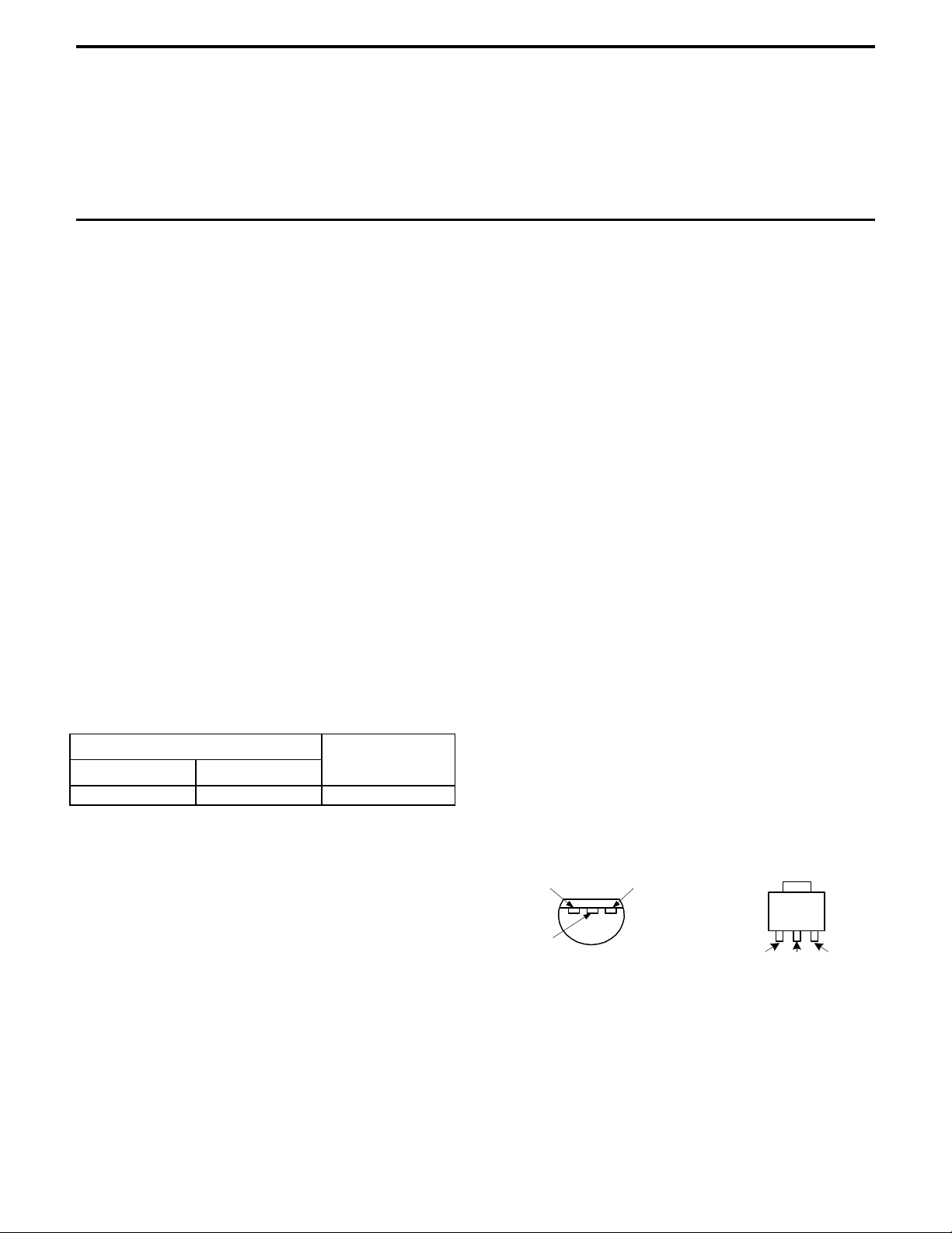
ORDERING INFORMATION PIN CONNECTIONS
PACKAGE TYPE OPER. TEMP
TO-92 SOT-89
AMS116N-X AMS116L-X IND
X =5V
*For additional available fixed voltages contact factory
RANGE
• Toys
• Low Voltage Systems
TO-92
Plastic Package (N)
OUTPUT
GND
Bottom View
INPUT
SOT-89 Package
(L)
123
OUTPUTGNDINPUT
Top View
Advanced Monolithic Systems, Inc.
AMS116
http://www.BDTIC.com/AMS
ABSOLUTE MAXIMUM RATINGS (Note 1)
Input Voltage 18V Maximum Junction Temperature
Operating Voltage Range 2.5V to 16V Storage Temperature
-65°C to +150°C
Load Current 150mA Lead Temperature (Soldering 25 sec)
Internal Power Dissipation Internally Limited ESD 2000V
ELECTRICAL CHARACTERISTICS
Electrical Characteristics at TJ=25°C, C2 = 100µF unless otherwise specified.
PARAMETER
Output Voltage VIN = V
CONDITIONS
(Note 2)
+3V -3 +3 %
OUT
Min.
AMS116-X
Typ.
Max.
+125°C
265°C
Units
Line Regulation VIN = V
Load Regulation
Dropout Voltage
Quiescent Current
Ripple Rejection fO = 120Hz 80 dB
Temperature Coefficient
Note 1: Absolute Maximum Ratings are limits beyond which damage to the device may occur. For guaranteed performance limits and associated test
conditions, see the Electrical Characteristics tables.
Note 2: See Circuit in Typical Applications. To ensure constant junction temperature, low duty cycle pulse testing is used.
Note 3: Limits appearing in boldface type apply over the entire junction temperature range for operation. Limits appearing in normal type apply for T
25°C.
5mA ≤I
IO ≤ 30 mA
IO = 100 mA
IO ≤ 10 mA, V
IO ≤ 10 mA, V
+3V to 14V 2 30 mV
OUT
≤ 100 mA
O
IN
IN
= V
= V
+3V to 14V
OUT
+3V to 14V
OUT
15 60 mV
80
170
400 1000
±.35
150
330
mV
mV
µA
mV/°C
= TJ =
A
V
IN
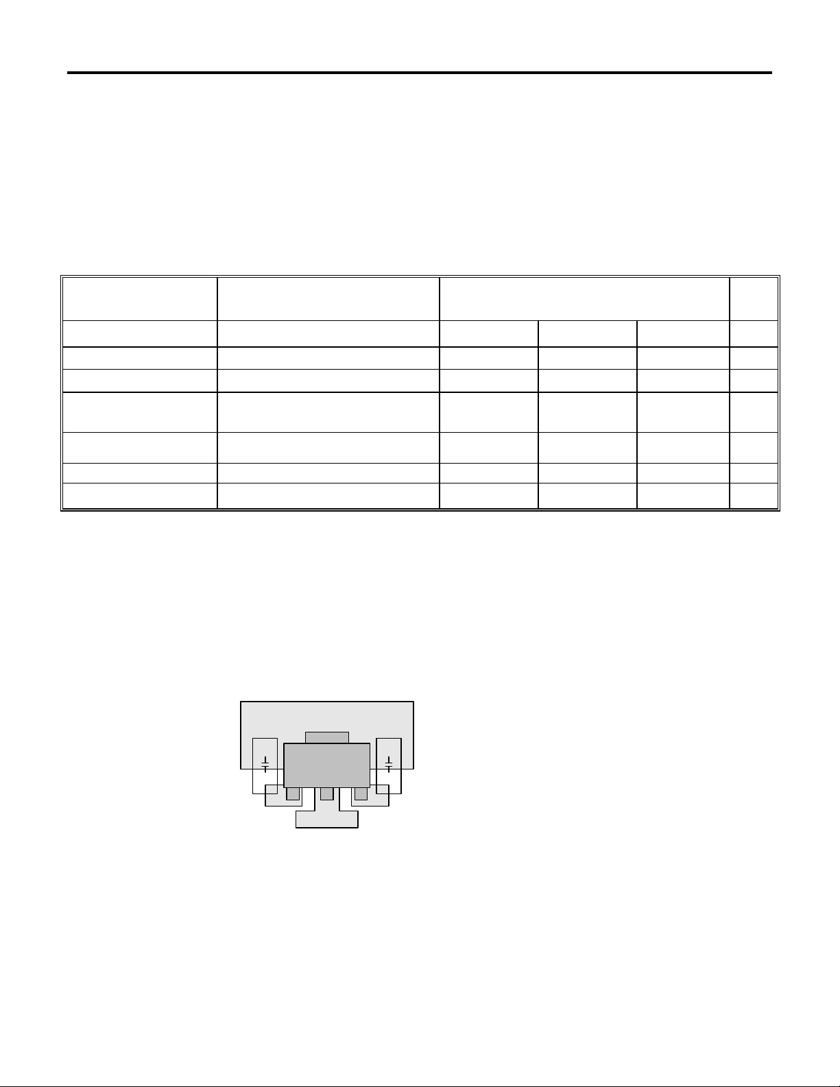
Figure 1. SOT-89 Board Layout
Advanced Monolithic Systems, Inc.
++
V
OUT
http://www.BDTIC.com/AMS
APPLICATION HINTS
Package Power Dissipation
The package power dissipation is the level at which the thermal
sensor monitoring the junction temperature is activated. The
AMS116 shuts down when the junction temperature exceeds the
limit of 150°C. The junction temperature rises as the difference
between the input power and output power increases. The
mounting pad configuration on the PCB, the board material, as
well as the ambient temperature affect the rate of temperature rise.
The junction temperature will be low, even if the power
dissipation is high, when the mounting of the device has good
thermal conductivity. When mounted on the recommended
mounting pad (figure1) the power dissipation for the SOT-89
package is 600mW. For operation above 25°C derate the power
dissipation at 4.8mW/°C. To determine the power dissipation for
shutdown when mounted, attach the device on the PCB and
increase the input-to-output voltage until the thermal protection
circuit is activated. Calculate the power dissipation of the device
by subtracting the output voltage from the input voltage and
multiply by the output current. The measurements should allow
for the ambient temperature of the PCB. The value obtained from
P
/ (150°C - TA) is the derating factor. The PCB mounting pad
D
should provide maximum thermal conductivity in order to
maintain low device temperatures. As a general rule, the lower the
temperature, the better the reliability of the device.
The thermal resistance when the device is mounted is equal to:
T
= θJA x PD + T
J
A
The internal limit for junction temperature is 150°C. If the ambient
temperature is 25°C, then:
150°C = θ
θ
JA
A simple way to determine PD is to calculate V
x PD + 25°C
JA
= 125°C/ P
D
x IIN when the
IN
output is shorted. As the temperature rises, the input gradually will
decrease. The P
value obtained when the thermal equilibrium is
D
reached, is the value that should be used.
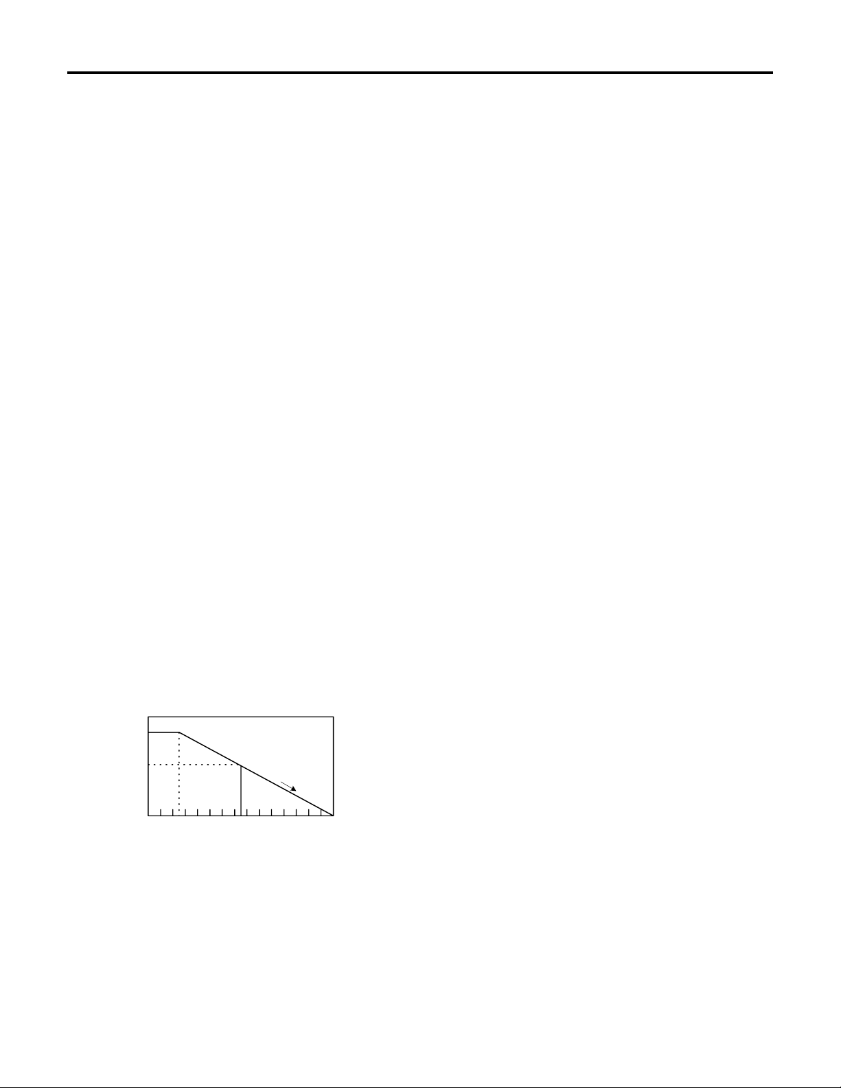
The range of usable currents can be found from the graph in figure
2.
(mW)
P
D
D
PD
3
6
5
75 15025 50
T (°C)
4
Figure 2
Procedure:
1. Find P
2. P
.
D
is calculated as PD x (0.8 - 0.9).
D1
3. Plot PD1 against 25°C.
4. Connect PD1 to the point corresponding to the 150°C.
AMS116
5. Take a vertical line from the maximum operating temperature
(75°C) to the derating curve.
6. Read the value of P
intersects the derating curve. This is the maximum power
dissipation, D
PD
The maximum operating current is:
I
= (DPD/ (V
OUT
External Capacitors
The AMS116 series require an output capacitor for device
stability. The value required depends on the application circuit
and other factors.
Because high frequency characteristics of electrolytic capacitors
depend greatly on the type and even the manufacturer, the value
of capacitance that works well with AMS116 for one brand or
type may not necessary be sufficient with an electrolytic of
different origin. Sometimes actual bench testing will be the only
means to determine the proper capacitor type and value. To obtain
stability in all general applications a high quality 100µF
aluminum electrolytic or a 47µF tantalum electrolytic can be used.
A critical characteristic of the electrolytic capacitors is their
performance over temperature. The AMS116 is designed to
operate to -40°C, but some electrolytics will freeze around -30°C
therefore becoming ineffective. In such case the result is
oscillation at the regulator output. For all application circuits
where cold operation is necessary, the output capacitor must be
rated to operate at the minimum temperature. In applications
where the regulator junction temperature will never be lower than
25°C the output capacitor value can be reduced by a factor of two
over the value required for the entire temperature range (47µF for
a high quality aluminum or 22µF for a tantalum electrolytic
capacitor).
With higher output currents, the stability of AMS116 decreases.
Considering the fact that in many applications the AMS116 is
operated at only a few milliamps (or less) of output current, the
output capacitor value can be reduced even further. For example,
a circuit that is required to deliver a maximum of 10mA of output
current from the regulator output will need an output capacitor of
only half the value compared to the same regulator required to
deliver the full output current of 100mA.
As a general rule, with higher output voltages the value of the
output capacitance decreases, since the internal loop gain is
reduced.
In order to determine the minimum value of the output capacitor,
for an application circuit, the entire circuit including the capacitor
should be bench tested at minimum operating temperatures and
maximum operating currents. To maintain internal power
dissipation and die heating to a minimum, the input voltage should
be maintain at 0.6V above the output. Worst-case occurs just after
input power is applied and before the die had the chance to heat
up. After the minimum capacitance value has been found for the
specific brand and type of electrolytic capacitor, the value should
be doubled for actual use to cover for production variations both
in the regulator and the capacitor.
at the point where the vertical line
D
.
- VO)
IN(MAX)
Advanced Monolithic Systems, Inc.

http://www.BDTIC.com/AMS
TYPICAL PERFORMANCE CHARACTERISTICS
Dropout Voltage
0.6
0.5
0.4
0.3
0.2
0.1
IO = 100mA
IO = 50mA
IO = 10mA
Dropout Voltage
1.2
1.0
0.8
0.6
0.4
0.2
AMS116
Line Transient Response
V
= V
3
2
1
0
-1
DEVIATION (mV)
-2
OUTPUT VOLTAGE
~
~
-3
3
IN
OUT
C2= 100 µF
= 9V
~
~
INPUT OUTPUT DIFFERENTIAL (V)
0
040
JUNCTION TEMPERATURE (° C)
Load Transient Response
C2= 100µF
40
0
DEVIATION (mV)
-40
OUTPUT VOLTAGE
~
~
150
0
LOAD CURRENT(mA)
QUIESCENT CURRENT (mA)
0153045
Quiescent Current
25
20
15
10
~
~
3
2
1
0
-40 40 80 120
TIME (µs)
0
TEMPERATURE (° C)
80
IO = 50mA
IO = 0mA
120
~
~
~
~
INPUT OUTPUT DIFFERENTIAL (V)
0
050
OUTPUT CURRENT (mA)
Peak Output Current
300
250
200
150
100
50
OUTPUT CURRENT (mA)
0
010
35
30
25
20
15
10
5
0
QUIESCENT CURRENT (mA)
-5
-20 -10 0 10 20 30 40 50 60
TJ= 25°C
TJ = 85°C
TJ = -40°C
20
INPUT VOLTAGE (V)
Quiescent Current
IO= 100mA
IO= 50mA
IO= 10mA
INPUT VOLTAGE (V)
100
30
CHANGE (V)
0
INPUT VOLTAGE
QUIESCENT CURRENT (mA)
RIPPLE REJECTION (dB)
0153045
Quiescent Current
30
VIN = 14V
25
20
15
10
5
0
030
Ripple Rejection
85
80
75
70
65
60
55
IO= 10mA
50
45
1 10 100 1k 10k 100k 1M
TIME (µs)
60
OUTPUT CURRENT (mA)
C2 = 100µF
ALUM
FREQUENCY (Hz)
90
C2 = 100µF
TANTALUM

http://www.BDTIC.com/AMS
AMS116
TYPICAL PERFORMANCE CHARACTERISTICS (Continued)
Ripple Rejection
85
80
75
70
65
60
55
RIPPLE REJECTION (dB)
FQ= 120Hz
50
45
0 25 50 75 100
OUTPUT CURRENT (mA)
Ripple Rejection
85
80
75
70
65
60
55
RIPPLE REJECTION (dB)
FQ= 120Hz
50
45
0 25 50 75 100
OUTPUT CURRENT (mA)
Output Capacitor ESR
)
100
Ω
10
1
0.1
0.01
0 20 40 60 100
EQUIVALENT SERIES RESISTANCE (
OUTPUT CURRENT (mA)
STABLE
REGION
C
OUT
VO = 5V
= 100µF
80
Maximum Power Dissipation (TO-92)
1.0
0.9
0.8
0.7
0.6
0.5
0.4
0.3
0.2
POWER DISSIPATION (W)
0.1
0.4" Lead
Lenght from
PC Board
0
10 20 30 40 50 60 70 800
AMBIENT TEMPERATURE (° C)
0.125" Lead Lenght
from PC Board
Maximum Power Dissipation (SOT-89)
1.0
0.9
0.8
0.7
0.6
0.5
0.4
0.3
0.2
POWER DISSIPATION (W)
0.1
UNMOUNTED
0
10 20 30 40 50 60 70 800
AMBIENT TEMPERATURE (° C)
MOUNTED
ON PCB
90

http://www.BDTIC.com/AMS
TYPICAL APPLICATIONS
Voltage Regulator Circuit Voltage Boost Circuit
UNREGULATED
INPUT
IN
C1*
µ
F
0.1
AMS116
GND
I
Q
V
*Required if regulator is located far from power supply filter.
**C2 must be at least 100µF to maintain stability; it can be increased
without bound to maintain regulation during transients and it should be
located as close as possible to the regulator. This capacitor must be rated
over the same operating temperature range like the regulator. The ESR
of this capacitor is critical (see curve).
Current Boost Circuit
100
AMS116
10
µ
F
GND
++
47µF
C2**
100
V
OUT
REGULATED
OUTPUT
µ
F
AMS116
AMS116
++
V
µ
F
1
O
I
Q
R
= VO+IQR
V
OUT
Current Regulator Circuit
AMS116
V
IN
1
V
µ
F
O
47µF
V
OUT
I
O
R
++
47µF
I
Q
= (VO/R )+ I
I
O
Q

http://www.BDTIC.com/AMS
PACKAGE DIMENSIONS inches (millimeters) unless otherwise noted.
3 LEAD TO-92 PLASTIC PACKAGE (N)
0.060±0.005
(1.524±0.127)
DIA
0.180±0.005
(4.572±0.127)
0.180±0.005
(4.572±0.127)
0.90
(2.286)
NOM
0.060±0.010
(1.524±0.254)
AMS116
0.140±0.010
(3.556±0.127)
10°
NOM
N (TO-92 ) AMS DRW# 042391
0.500
(12.70)
MIN
0.050±0.005
(1.270±0.127)
UNCONTROLLED
0.050
(1.270)
LEAD DIMENSIONS
MAX
0.016±0.003
(0.406±0.076)
5° NOM
0.015±0.002
(0.381±0.051)
SOT-89 PLASTIC PACKAGE (L)
0.173-0.181
0.155-0.167
(3.94-4.25)
0.090-0.102
(2.29-2.60)
(4.40-4.60)
0.064-0.072
(1.62-1.83)
0.055-0.063
(1.40-1.60)
0.084-0.090
(2.13-2.29)
0.014-0.017
(0.35-0.44)
0.059
(1.50)
BSC
0.118
(3.00)
BSC
0.017-0.022
(0.44-0.56)
0.035-0.047
(0.89-1.20)
0.014-0.019
(0.36-0.48)
L (SOT-89 ) AMS DRW# 042392
 Loading...