

http://www.BDTIC.com/AMS
Advanced AMS1085
Monolithic 3A LOW DROPOUT VOLTAGE REGULATOR
Systems
RoHS compliant
FEATURES APPLICATIONS
•••• Three Terminal Adjustable or Fixed Voltages •••• High Efficiency Linear Regulators
1.5V, 2.5V, 2.85V, 3.0V, 3.3V, 3.5V and 5.0V
•••• Output Current of 3A •••• Microprocessor Supply
•••• Operates Down to 1V Dropout •••• Battery Chargers
•••• Load Regulation: 0.1% •••• Constant Current Regulators
•••• Line Regulation: 0.015% •••• Notebook/Personal Computer Supplies
•••• TO-220, TO-263 and TO-252 packages available •••• Portable Instrumentation
GENERAL DESCRIPTION
The AMS1085 series of adjustable and fixed voltage regulators are designed to provide 3A output current and to operate down
to 1V input-to-output differential. The dropout voltage of the device is guaranteed maximum 1.3V at maximum output current,
decreasing at lower load currents.
On-chip trimming adjusts the reference voltage to 1%. Current limit is also trimmed, minimizing the stress under overload
conditions on both the regulator and power source circuitry.
The AMS1085 devices are pin compatible with older three-terminal regulators and are offered in 3 lead TO-220 package, 3 and
2 lead TO-263 (Plastic DD) and TO-252 (D PAK) package.
ORDERING INFORMATION:
3 LEAD TO-220 2&3 LEAD TO-263 TO-252
AMS1085CT AMS1085CM AMS1085CD
AMS1085CT-1.5 AMS1085CM-1.5 AMS1085CD-1.5
AMS1085CT-2.5 AMS1085CM-2.5 AMS1085CD-2.5
AMS1085CT-2.85 AMS1085CM-2.85 AMS1085CD-2.85
AMS1085CT-3.0 AMS1085CM-3.0 AMS1085CD-3.0
AMS1085CT-3.3 AMS1085CM-3.3 AMS1085CD-3.3
AMS1085CT-3.5 AMS1085CM-3.5 AMS1085CD-3.5
AMS1085CT-5.0 AMS1085CM-5.0 AMS1085CD-5.0
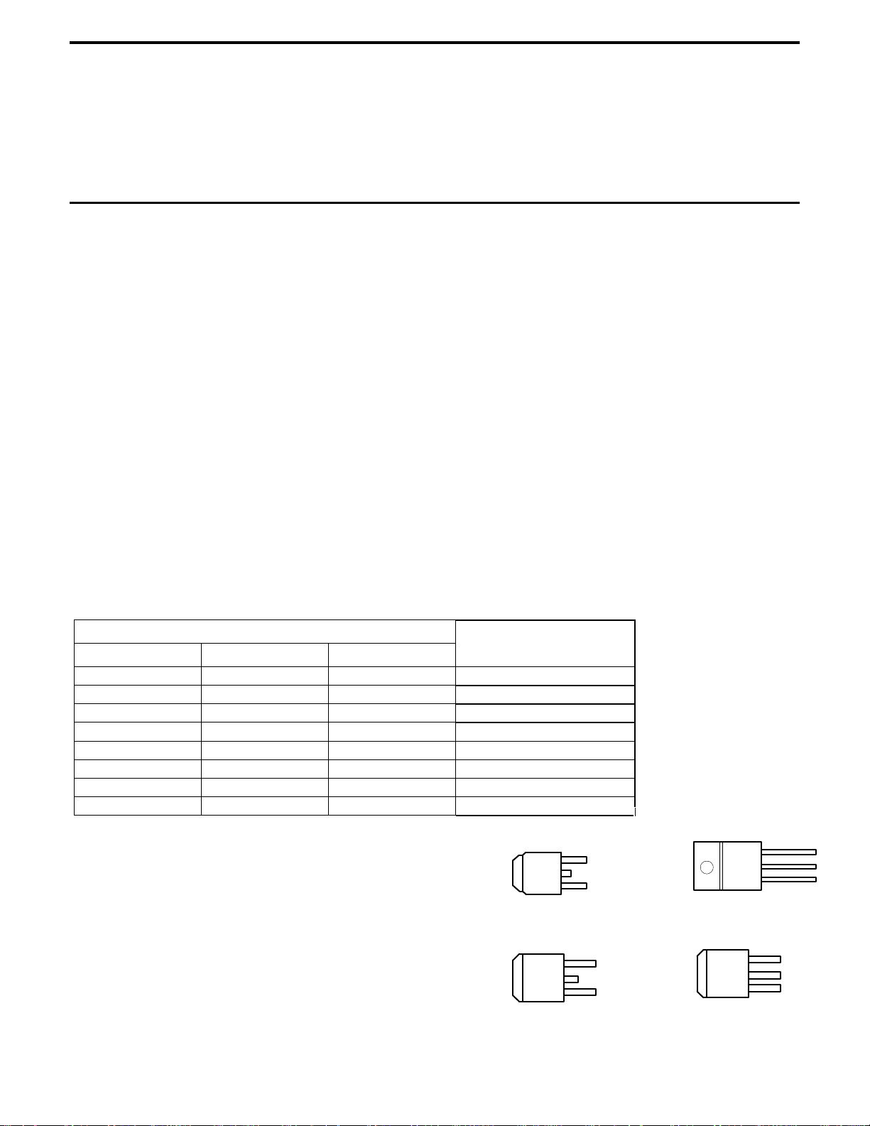
PIN CONNECTIONS
FIXED VERSION
1- Ground
2- V
3-
OUT
VIN
PACKAGE TYPE OPERATING JUNCTION
ADJUSTABLE VERSION
1- Adjust
2- V
OUT
3- VIN
••••
Post Regulators for Switching Supplies
TEMPERATURE RANGE
0 to 125° C
0 to 125° C
0 to 125° C
0 to 125° C
0 to 125° C
0 to 125° C
0 to 125° C
0 to 125° C
TO-220 FRONT VIEW
TO-252 FRONT VIEW
3
2
1
3
2
1
TAB IS
OUTPUT
2L TO-263 FRONT VIEW
TAB IS
OUTPUT
3
2
1
OUTPUT
TAB IS
3L TO-263 FRONT VIEW
3
2
1
TAB IS
OUTPUT
Advanced Monolithic Systems, Inc.

http://www.BDTIC.com/AMS
ABSOLUTE MAXIMUM RATINGS (Note 1)
Power Dissipation Internally limited Soldering information
Input Voltage 15V Lead Temperature (25 sec)
Operating
Control Section
Power Transistor
Storage temperature
Junction Temperature R
0°C to 125°C
0°C to 150°C
- 65°C to +150°C
Thermal Resistance
TO-220 package
TO-263 package
TO-252 package
* With package soldering to 0.5in
ground plane or internal power plane ϕ
20°C/W to >40°C/W depending on mounting technique.
2
copper area over backside
ELECTRICAL CHARACTERISTICS
Electrical Characteristics at I
= 0 mA, and TJ = +25°C unless otherwise specified.
OUT
AMS1085
265°C
ϕ JA= 50°C/W
ϕ JA= 30°C/W *
ϕ JA= 100°C/W
can vary from
JA
Parameter
Device Conditions Min Typ Max Units
Reference Voltage
(Note 2)
Output Voltage
(Note 2)
AMS1085-2.5
Line Regulation AMS1085/-1.5/-2.5/-
Load Regulation
(Notes 2, 3)
AMS1085-1.5
AMS1085-2.5
AMS1085-2.85
AMS1085-3.0
AMS1085-3.3
AMS1085-3.5
AMS1085-5.0
AMS1085 I
AMS1085-1.5
AMS1085-2.85
AMS1085-3.0
AMS1085-3.3
AMS1085-3.5
AMS1085-5.0
2.85/ -3.0/-3.3/-3.5/-5.0
AMS1085
= 10 mA
OUT
10mA ≤ I
0 ≤ I
0 ≤ I
0 ≤ I
0 ≤ I
0 ≤ I
0 ≤ I
0 ≤ I
I
LOAD
(VIN - V
VIN = 5V, 0 ≤ I
VIN = 5V, 0 ≤ I
VIN = 5V, 0 ≤ I
VIN = 5V, 0 ≤ I
VIN = 5V, 0 ≤ I
VIN = 5.25V, 0 ≤ I
VIN = 8V, 0 ≤ I
≤ 3A, 1.5V≤ (VIN - V
OUT
≤ 3A , 3V≤ VIN ≤ 12V
OUT
≤ 3A , 4V≤ VIN ≤ 12V
OUT
≤ 3A , 4.35V≤ VIN ≤ 12V
OUT
≤ 3A , 4.5V ≤ VIN ≤ 12V
OUT
≤ 3A , 4.75V ≤ VIN ≤ 12V
OUT
≤ 3A , 5V ≤ VIN ≤ 12V
OUT
≤ 3A , 6.5V ≤ VIN ≤ 12V
OUT
= 10 mA , 1.5V≤ (VIN - V
) =3V, 10mA ≤ I
OUT
OUT
OUT
OUT
OUT
OUT
OUT
≤ 3A
≤ 3A
≤ 3A
≤ 3A
≤ 3A
≤ 3A
OUT
≤ 3A
OUT
OUT
OUT
≤ 3A
) ≤ 12V
) ≤ 12V
1.238
1.225
1.485
1.470
2.475
2.450
2.82
2.79
2.970
2.940
3.267
3.235
3.465
3.430
4.950
4.900
0.3
3
3
3
3
3
3
5
1.250
1.250
1.500
1.500
2.500
2.500
2.850
2.850
3.000
3.000
3.300
3.300
3.500
3.500
5.000
5.000
0.6
0.1
0.2
6
6
6
6
7
6
10
1.262
1.270
1.515
1.530
2.525
2.550
2.88
2.91
3.300
3.360
3.333
3.365
3.535
3.570
5.050
5.100
10
10
0.3
0.4
12
20
12
20
12
20
12
20
15
25
15
25
20
35
V
V
V
V
V
V
V
V
V
V
V
V
V
V
V
mV
mV
%
%
mV
mV
mV
mV
mV
mV
mV
mV
mV
mV
mV
mV
mV
mV
Dropout Voltage
(V
- V
OUT
)
IN
AMS1085/-1.5/-2.5/-
2.85/ -3.0/-3.3/-3.5/-5.0
Advanced Monolithic Systems, Inc.
∆V
OUT
, ∆V
REF
= 1%, I
= 3 A (Note 4)
OUT
1.2 1.3
V

http://www.BDTIC.com/AMS
ELECTRICAL CHARACTERISTICS
Electrical Characteristics at I
= 0 mA, and TJ = +25°C unless otherwise specified.
OUT
AMS1085
Parameter
Device Conditions Min Typ Max Units
Current Limit
Minimum Load
Current
Quiescent Current AMS1085/-1.5/-2.5/-
Ripple Rejection AMS1085
AMS1085-1.5
AMS1085-2.5
AMS1085-2.85
AMS1085-3.0
AMS1085-3.3
AMS1085-3.5
AMS1085-5.0
Thermal Regulation AMS1085 TA = 25°C, 30ms pulse 0.008 0.04 %W
AMS1085/-1.5/-2.5/-
2.85/ -3.0/-3.3/-3.5/-5.0
(VIN - V
AMS1085 (VIN - V
VIN ≤ 12V
2.85/ -3.0/-3.3/-3.5/-5.0
f =120Hz , C
(VIN-V
f =120Hz , C
VIN = 4.5V
f =120Hz , C
VIN = 5.5V
f =120Hz , C
VIN = 6V
f =120Hz , C
VIN = 6V
f =120Hz , C
VIN = 6.3V
f =120Hz , C
VIN = 6.5V
f =120Hz , C
VIN = 8V
) = 5V
OUT
) = 12V (Note 5)
OUT
OUT
= 25µF Tantalum, I
OUT
) = 3V, C
ADJ
= 25µF Tantalum, I
OUT
= 25µF Tantalum, I
OUT
= 25µF Tantalum, I
OUT
= 25µF Tantalum, I
OUT
= 25µF Tantalum, I
OUT
= 25µF Tantalum, I
OUT
= 25µF Tantalum, I
OUT
=25µF
OUT
OUT
OUT
OUT
OUT
OUT
OUT
OUT
= 3A,
= 3A,
= 3A,
= 3A,
= 3A
= 3A
= 3A
= 3A
3.00 3.50 4.00
5 10
60 75
60
60
60
60 72
60 72
60 72
60 68
72
72
72
5
10
dB
A
mA
mA
dB
dB
dB
dB
dB
dB
dB
Adjust Pin Current AMS1085
Adjust Pin Current
AMS1085
Change
Temperature Stability
10mA ≤ I
10mA ≤ I
≤ 3A , 1.5V≤ (VIN - V
OUT
≤ 3A , 1.5V≤ (VIN - V
OUT
OUT
OUT
) ≤ 12V
) ≤12V
55
0.2
0.5
120
5
µA
µA
µA
%
Long Term Stability TA =125°C, 1000Hrs 0.3 1 %
RMS Output Noise
(% of V
OUT
)
Thermal Resistance
Junction-to-Case
TA = 25°C , 10Hz ≤ f ≤ 10kHz
M Package: Control Circuitry/ Power Transistor
T Package: Control Circuitry/ Power Transistor
0.003
1.5/4.0
1.5/4.0
°C/W
°C/W
%
Parameters identified with boldface type apply over the full operating temperature range.
Note 1: Absolute Maximum Ratings indicate limits beyond which damage to the device may occur. For guaranteed specifications and test conditions, see the
Electrical Characteristics. The guaranteed specifications apply only for the test conditions listed.
Note 2: Line and Load regulation are guaranteed up to the maximum power dissipation of 15W. Power dissipation is determined by the input/output
differential and the output current. Guaranteed maximum power dissipation will not be available over the full input/output range.
Note 3: See thermal regulation specifications for changes in output voltage due to heating effects. Line and load regulation are measured at a constant
junction temperature by low duty cycle pulse testing. Load regulation is measured at the output lead ~1/8” from the package.
Note 4: Dropout voltage is specified over the full output current range of the device.
Note 5: Minimum load current is defined as the minimum output current required to
to regulate if the output current is greater than 10mA.
maintain regulation. When (VIN - V
) = 12V the device is guaranteed
OUT
Advanced Monolithic Systems, Inc.

http://www.BDTIC.com/AMS
APPLICATION HINTS
The AMS1085 series of adjustable and fixed regulators are easy to
use and have all the protection features expected in high
performance voltage regulators: short circuit protection and
thermal shutdown.
Pin compatible with older three terminal adjustable regulators,
these devices offer the advantage of a lower dropout voltage, more
precise reference tolerance and improved reference stability with
temperature.
Stability
The circuit design used in the AMS1085 series requires the use of
an output capacitor as part of the device frequency compensation.
The addition of 150µF aluminum electrolytic or a 22µF
tantalum on the output will ensure stability for all operating
conditions.
When the adjustment terminal is bypassed to improve the ripple
rejection, the requirement for an output capacitor increases. The
value of 22µF tantalum or 150µF aluminum covers all cases of
bypassing the adjustment terminal. Without bypassing the
adjustment terminal smaller capacitors can be used with equally
good results.
To ensure good transient response with heavy load current changes
capacitor values on the order of 100µF are used in the output of
many regulators. To further improve stability and transient
response of these devices larger values of output capacitor can be
used.
Protection Diodes
Unlike older regulators, the AMS1085 family does not need any
protection diodes between the adjustment pin and the output and
from the output to the input to prevent over-stressing the die.
Internal resistors are limiting the internal current paths on the
AMS1085 adjustment pin, therefore even with capacitors on the
adjustment pin no protection diode is needed to ensure device
safety under short-circuit conditions.
Diodes between the input and output are not usually needed.
Microsecond surge currents of 50A to 100A can be handled by the
internal diode between the input and output pins of the device. In
normal operations it is difficult to get those values of surge
currents even with the use of large output capacitances. If high
value output capacitors are used, such as 1000µF to 5000µF and
the input pin is instantaneously shorted to ground, damage can
occur. A diode from output to input is recommended, when a
crowbar circuit at the input of the AMS1085 is used. Normal
power supply cycling or even plugging and unplugging in the
system will not generate current large enough to do any damage.
The adjustment pin can be driven on a transient basis ±25V, with
respect to the output without any device degradation. As with any
IC regulator, none the protection circuitry will be functional and
the internal transistors will break down if the maximum input to
output voltage differential is exceeded.
solid
AMS1085
D1
V
IN
Overload Recovery
When the power is first turned on, as the input voltage rises, the
output follows the input, permitting the regulator to start up into
heavy loads. During the start-up, as the input voltage is rising, the
input-to-output voltage differential remains small, allowing the
regulator to supply large output currents. A problem can occur
with a heavy output load when the input voltage is high and the
output voltage is low, when the removal of an output short will
not permit the output voltage to recover. The load line for such a
load may intersect two points on the output current curve. In this
case, there are two stable output operating points for the regulator.
With this double intersection, the power supply may need to be
cycled down to zero and brought up again to make the output
recover.
Ripple Rejection
The ripple rejection values are measured with the adjustment pin
bypassed. The impedance of the adjust pin capacitor at the ripple
frequency should be less than the value of R1 (normally 100Ω
to120Ω) for a proper bypassing and ripple rejection approaching
the values shown. The size of the required adjust pin capacitor is a
function of the input ripple frequency. If R1=100Ω at 120Hz the
adjust pin capacitor should be 25µF. At 10kHz only 0.22µF is
needed.
The ripple rejection will be a function of output voltage, in circuits
without an adjust pin bypass capacitor. The output ripple will
increase directly as a ratio of the output voltage to the reference
voltage (V
Output Voltage
The AMS1085 series develops a 1.25V reference voltage between
the output and the adjust terminal. Placing a resistor between these
two terminals causes a constant current to flow through R1 and
down through R2 to set the overall output voltage.
OUT
/ V
IN OUT
).
REF
AMS1085
ADJ
C
10µF
ADJ
+
R
1
R
2
C
OUT
150µF
V
OUT
Advanced Monolithic Systems, Inc.

http://www.BDTIC.com/AMS
APPLICATION HINTS
This current is normally the specified minimum load current of
10mA. Because I
error and it can usually be ignored.
V
IN
Load Regulation
True remote load sensing it is not possible to provide, because the
AMS1085 is a three terminal device. The resistance of the wire
connecting the regulator to the load will limit the load regulation.
The data sheet specification for load regulation is measured at the
bottom of the package. Negative side sensing is a true Kelvin
connection, with the bottom of the output divider returned to the
negative side of the load.
The best load regulation is obtained when the top of the resistor
divider R1 is connected directly to the case not to the load. If R1
were connected to the load, the effective resistance between the
regulator and the load would be:
R
R1
P
V
IN
is very small and constant it represents a small
ADJ
AMS1085
IN OUT
ADJ
I
ADJ
50µA
V
= V
OUT
(1+ R2/R1)+I
REF
V
REF
R2
ADJ
Figure 1. Basic Adjustable Regulator
x ( R2+R1 ) , R
AMS1085
IN OUT
ADJ
= Parasitic Line Resistance
P
R
P
PARASITIC
LINE RESISTANCE
R1
R2
V
OUT
AMS1085
Con
nected as shown, R
Using 16-gauge wire the parasitic line resistance is about 0.004Ω
per foot, translating to 4mV/ft at 1A load current. It is important to
keep the positive lead between regulator and load as short as
possible and use large wire or PC board traces.
Thermal Considerations
The AMS1085 series have internal power and thermal limiting
circuitry designed to protect the device under overload conditions.
However maximum junction temperature ratings should not be
exceeded under continuous normal load conditions. Careful
consideration must be given to all sources of thermal resistance
from junction to ambient, including junction-to-case, case-to-heat
sink interface and heat sink resistance itself. To ensure safe
operating temperatures and reflect more accurately the device
temperature, new thermal resistance specifications have been
developed. Unlike older regulators with a single junction-to-case
thermal resistance specification, the data section for these new
regulators provides a separate thermal resistance and maximum
junction temperature for both the Control Section and the Power
Transistor. Calculations for both temperatures under certain
conditions of ambient temperature and heat sink resistance and to
ensure that both thermal limits are met.
Junction-to-case thermal resistance is specified from the IC
junction to the bottom of the case directly below the die. This is
the lowest resistance path for the heat flow. In order to ensure the
best possible thermal flow from this area of the package to the
heat sink proper mounting is required. Thermal compound at the
case-to-heat sink interface is recommended. A thermally
conductive spacer can be used, if the case of the device must be
electrically isolated, but its added contribution to thermal
resistance has to be considered.
not multiplied by the divider ratio.
P is
R1*
R2*
*CONNECT R1 TO CASE
CONNECT R2 TO LOAD
Figure 2. Connections for Best Load Regulation
Advanced Monolithic Systems, Inc.
R
L

http://www.BDTIC.com/AMS
TYPICAL PERFORMANCE CHARACTERISTICS
Dropout Voltage
2
TJ =25° C
1
0.10
0.05
0
-0.05
Load Regulation
∆
I = 3A
AMS1085
Temperature Stability
2.0
1.0
0
TJ =150° C
DIFFERENTIAL (V)
MINIMUM INPUT/OUTPUT
0
0 1 2 3 4
OUTPUT CURRENT (A)
Ripple Rejection
80
V
≤
3V
RIPPLE
70
P-P
60
50
40
(VIN-V
)≥V
OUT
30
DROPOUT
20
I
RIPPLE REJECTION (dB)
OUT=IFULL LOAD
10
0
100 1k 10k 100k
FREQUENCY (Hz)
Load Transient Response
0.3
0.2
0.1
C
= 0
ADJ
0
OUTPUT VOLTAGE
LOAD
DEVIATION (V)
CURRENT (A)
-0.1
-0.2
-0.3
~
~
3
2
1
0
0
CIN = 1µF
C
= 10µF TANTALUM
OUT
50
TIME (µs)
V
≤
0.5V
RIPPLE
P-P
(VIN-V
) ≥ 3V
OUT
V
= 10V
OUT
V
= 13V
IN
PRELOAD = 100mA
~
~
100
-0.10
-0.15
-0.20
OUTPUT VOLTAGE DEVIATION (%)
-50 -25 0 25 50 75 100 125 150
TEMPERATURE (° C)
Ripple Rejection vs. Current
100
90
80
70
fR = 120Hz
V
RIPPLE
60
fR =20kHz
50
V
≤
0.5V
RIPPLE
40
P-P
30
20
RIPPLE REJECTION (dB)
10
0
0
0.4 0.6 0.8 1.0
0.2
OUTPUT CURRENT (0 TO I
Line Transient Response
60
C
40
= 0
ADJ
20
0
-20
DEVIATION (mV)
-40
OUTPUT VOLTAGE
INPUT
-60
~
~
14
13
12
DEVIATION (V)
V
= 10V
OUT
IIN = 0.2A
CIN = 1µF TANTALUM
C
= 10µF TANTALUM
OUT
0 100
TIME (µs) CASE TEMPERATURE (° C)
≤
3V
-1.0
OUTPUT VOLTAGE CHANGE (%)
-2.0
-25 0 25 50 75 100 125 150
-50
TEMPERATURE (° C)
Short-Circuit Current
6
5
P-P
4
3
2
1
SHORT-CIRCUIT CURRENT (A)
0
) INPUT/OUTPUT DIFFERENTIAL (V)
FULL LOAD
0 2
4 6
Maximum Power Dissipation*
50
40
30
~
~
20
POWER (W)
10
0
200
506070
*AS LIMITED BY MAXIMUM JUNCTION TEMPERATURE
80 90
100
8 10 12
110
120 130 140 150
14
Advanced Monolithic Systems, Inc.

http://www.BDTIC.com/AMS
TYPICAL PERFORMANCE CHARACTERISTICS (Continued)
Minimum Operating Current
(Adjustable only)
10
9
8
7
6
5
4
3
2
1
0
0 2 4 6 8 10 12
MINIMUM OPERATING CURRENT (mA)
TJ = 150° C
TJ = 25° C
14 100
Adjust Pin Current
(Adjustable only)
100
90
A)
µ
80
70
60
50
40
30
20
ADJUST PIN CURRENT (
10
0
-50 -25
PACKAGE DIMENSIONS inches (millimeters) unless otherwise noted.
3 LEAD TO-220 PLASTIC PACKAGE (T)
0.165-0.180
(4.191-4.572)
0.460-0.500
(11.684-12.700)
0.390-0.415
(9.906-10.541)
0.147-0.155
(3.734-3.937)
0.230-0.270
(5.842-6.858)
0.330-0.370
(8.382-9.398)
DIA
0.570-0.620
(14.478-15.748)
0
TEMPERATURE (° C)INPUT/OUTPUT DIFFERENTIAL (V)
25 50 75
0.045-0.055
(1.143-1.397)
AMS1085
125
150
0.980-1.070
(24.892-27.178)
0.520-0.570
(13.208-14.478)
0.090-0.110
(2.286-2.794)
0.028-0.038
(0.711-0.965)
Advanced Monolithic Systems, Inc.
0.050
(1.270)
TYP
0.218-0.252
(5.537-6.401)
0.013-0.023
(0.330-0.584)
0.095-0.115
(2.413-2.921)
T (TO-220) AMS DRW# 042193

http://www.BDTIC.com/AMS
PACKAGE DIMENSIONS inches (millimeters) unless otherwise noted (Continued).
3 LEAD TO-263 PLASTIC DD (M)
0.390-0.415
(9.906-10.541)
0.060
(1.524)
TYP
0.330-0.370
(8.382-9.398)
0.165-0.180
(4.191-4.572)
0.004
(0.102 )
0.045-0.055
(1.143-1.397)
+0.008
-0.004
+0.203
-0.102
AMS1085
0.095-0.115
(2.413-2.921)
0.90-0.110
(2.29-2.79)
M (DD3) AMS DRW# 042191R1
0.090-0.110
(2.286-2.794)
0.032
(0.81)
TYP
0.199-0.218
(5.05-5.54)
0.108
(2.74)
TYP
0.013-0.023
(0.330-0.584)
2 LEAD TO-263 PLASTIC DD (M)
Advanced Monolithic Systems, Inc.

http://www.BDTIC.com/AMS
PACKAGE DIMENSIONS inches (millimeters) unless otherwise noted (Continued).
TO-252 PLASTIC PACKAGE (D)
0.255-0.265
0.380-0.410
(9.65-10.41)
(6.48-6.73)
0.206-0.214
(5.23-5.44)
0.235-0.245
(5.969-6.223)
0.087-0.094
(2.21-2.39)
7.0°
0.018-0.023
(0.46-0.58)
0.035-0.050
(0.89-1.27)
AMS1085
0.025
(0.635)
TYP
0.156-0.204
(3.96-5.18)
0.030
(0.762)
TYP
0.045-0.060
(1.14-1.52)
0.018-0.023
(0.46-0.58)
0.035-0.045
(0.89-1.14)
0.020±0.002
(0.510±0.0508)
D (D3) AMS DRW# 01160 1
Advanced Monolithic Systems, Inc.
 Loading...