

ADVANCED Monolithic System LP2950, LP2951 Service Manual
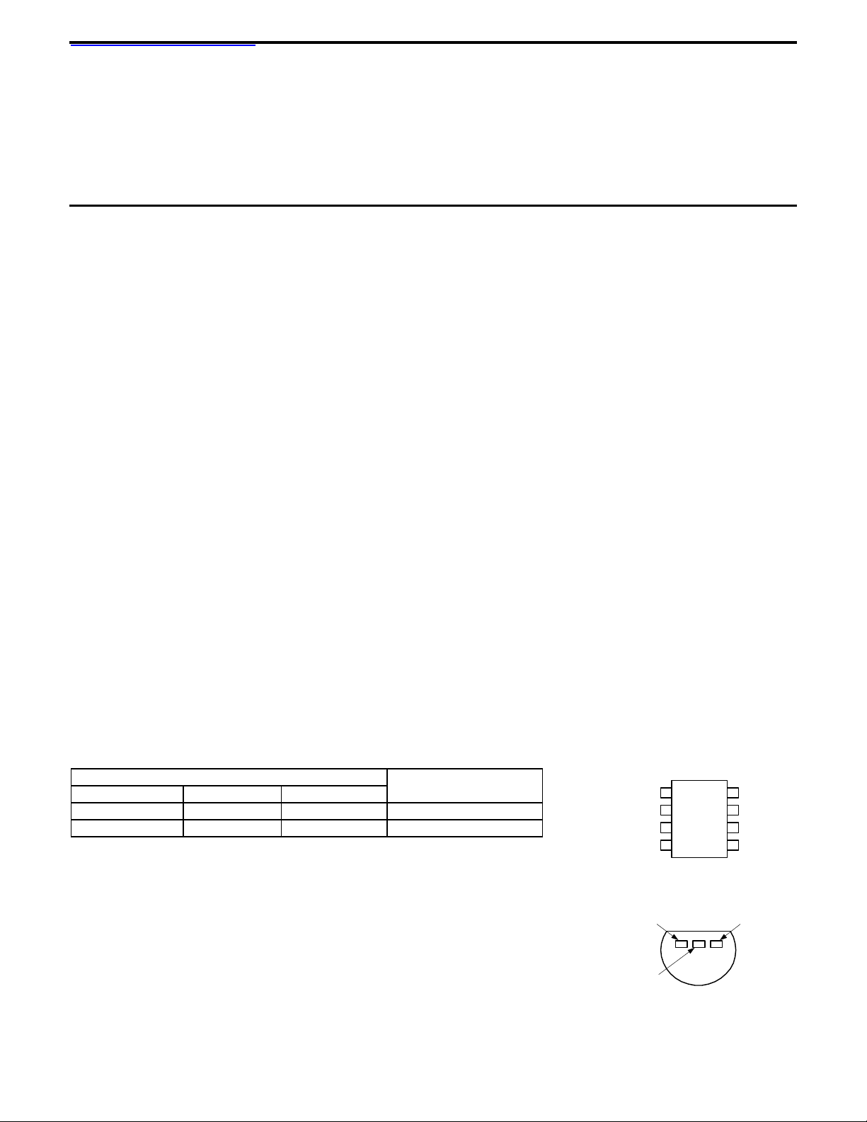
PACKAGE TYPE
OPERATING
TO-92
8 LEAD PDIP
8 LEAD SOIC
TEMP. RANGE
LP2950ACN-X
LP2951ACP-X
LP2951ACS-X
IND.
LP2950CN-X
LP2951CP-X
LP2951CS-X
IND
Bottom View
查询LP2950ACN-3供应商
Advanced LP2950/LP2951
Monolithic 100mA LOW DROPOUT VOLTAGE REGULATOR
Systems
FEATURES APPLICATIONS
•• 5V, 3.3V, and 3V Versions at 100mA Output Current •• Battery Powered Systems
•• High Accuracy Output Voltage •• Portable Consumer Equipment
•• Extremely Low Quiescent Current •• Cordless Telephones
•• Low Dropout Voltage •• Portable (Notebook) Computers
•• Extremely Tight Load and Line Regulation •• Portable Instrumentation
•• Very Low Temperature Coefficient •• Radio Control Systems
•• Current and Thermal Limiting •• Automotive Electronics
•• Needs Minimum Capacitance (1µµF) for Stability •• Avionics
•• Unregulated DC Positive Transients 60V •• Low-Power Voltage Reference
ADDITIONAL FEATURES (LP2951 ONLY)
•• 1.24V to 29V Programmable Output
•• Error Flag Warning of Voltage Output Dropout
•• Logic Controlled Electronic Shutdown
GENERAL DESCRIPTION
The LP2950 and LP2951 are micropower voltage regulators ideally suited for use in battery-powered systems. These devices
feature very low quiescent current (typ.75µA), and very low dropout voltage (typ.45mV at light loads and 380mV at 100mA)
thus prolonging battery life. The quiescent current increases only slightly in dropout. The LP2950/LP2951 has positive
transient protection up to 60V and can survive unregulated input transient up to 20V below ground.
The LP2950 and LP2951 were designed to include a tight initial tolerance (typ. 0.5%), excellent load and line regulation (typ.
0.05%), and a very low output voltage temperature coefficient, making these devices useful as a low-power voltage reference.
The LP2950 is offered in the 3-pin TO-92 package. LP2951 is available in 8-pin plastic SOIC and DIP packages and offers
three major additional system features. An error flag output warns of a low output voltage, often due to failing batteries on
input. The LP2951 also features the logic-compatible shutdown input which enables the regulator to be switched on and off.
The LP2951 device may be pin-strapped for a 5V, 3.3V, or 3V output, or programmed from 1.24V to 29V with an external
pair of resistors.
ORDERING INFORMATION PIN CONNECTION
8L SOIC/ 8L PDIP
X = 3.3V, or 3V
OUTPUT
SENSE
SHUTDOWN
GROUND
OUTPUT
1
2
3
4
Top View
TO-92
8
INPUT
7
FEEDBACK
6 V
TAP
5
ERROR
INPUT
Advanced Monolithic Systems, Inc. 6680B Sierra Lane, Dublin, CA 94568 Phone (925) 556-9090 Fax (925) 556-9140
GND
LP2950/LP2951
ABSOLUTE MAXIMUM RATINGS (Note 1)
Input Supply Voltage -0.3 to +30V Wave
SHUTDOWN Input Voltage, Infrared
Error Comparator Output Vapor Phase
Voltage,(Note 9) ESD TBD
FEEDBACK Input Voltage -1.5 to +30V
(Note 9) (Note 10)
OPERATING RATINGS (Note 1)
Power Dissipation Internally Limited
Junction Temperature
Storage Temperature
+150°C
-65°C to +150°C
Max. Input Supply Voltage 30V
Junction Temperature Range
Soldering Dwell Time, Temperature (TJ) (Note 8)
LP2950AC-XX, LP2950C-XX
LP2951AC-XX, LP2951C-XX
4 seconds, 260°C
4 seconds, 240°C
4 seconds, 219°C
-40°C to +125°C
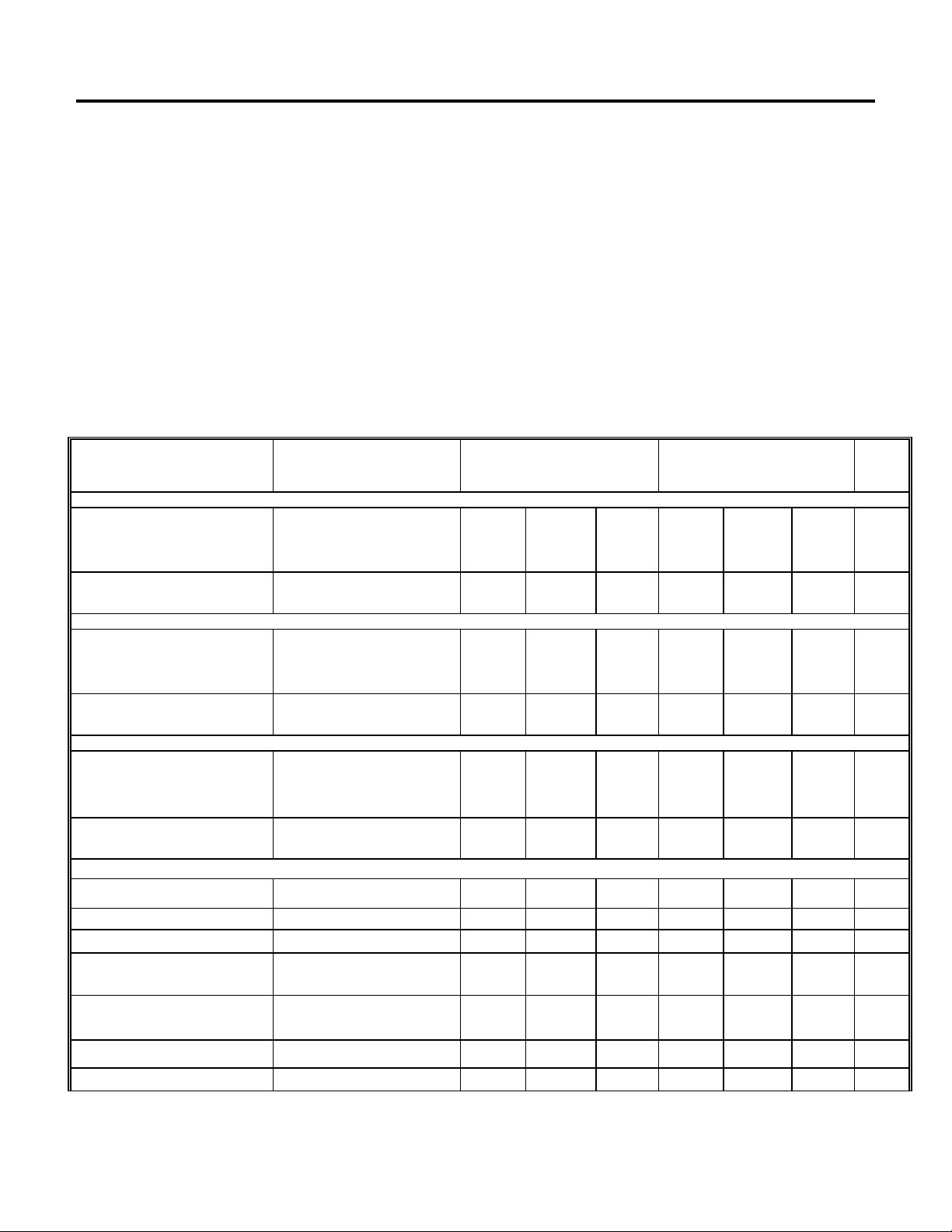
ELECTRICAL CHARACTERISTICS at V
Parameter Conditions
3 V Versions (Note 16)
Output Voltage
Output Voltage
3.3 V Versions (Note 16)
Output Voltage
Output Voltage
5 V Versions (Note 16)
Output Voltage
Output Voltage
All Voltage Options
Output Voltage
Temperature Coefficient (Note 12) (Note 4)
Line Regulation (Note 14)
Load Regulation (Note 14)
Dropout Voltage
(Note 5)
Ground Current
Current Limit
Thermal Regulation (Note 13) 0.05 0.2 0.05 0.2 %/W
TJ = 25°C (Note 3)
-25°C ≤TJ ≤85°C
Full Operating Temperature Range
100 µA ≤IL ≤100 mA
TJ ≤T
TJ = 25°C (Note 3)
-25°C ≤TJ ≤85°C
Full Operating Temperature Range
100 µA ≤IL ≤100 mA
TJ ≤T
TJ = 25°C (Note 3)
-25°C ≤TJ ≤85°C
Full Operating Temperature Range
100 µA ≤IL ≤100 mA
TJ ≤T
6V ≤Vin ≤30V (Note 15)
100 µA ≤IL ≤ 100 mA
IL = 100µ A
IL = 100 mA
IL = 100 µA
IL = 100 mA
V
out
(Note 2)
JMAX
JMAX
JMAX
= 0 160 200 160 200 mA
=Vout+1V, Ta=25°C, unless otherwise noted.
s
LP2950AC
LP2951AC
Min. Typ. Max.
2.985
2.970
2.964
2.958
3.284
3.267
3.260
3.254
4.975
4.95
4.94
4.925
3.0
3.0
3.0
3.0
3.3
3.3
3.3
3.3
5.0
5.0
5.0
5.0
20 50
0.03 0.1 0.04 0.2 %
0.04 0.1 0.1 0.2 %
50
380
75
8
3.015
3.030
3.036
3.042 2.928
3.317
3.333
3.340
3.346 3.221
5.025
5.050
5.06
5.075 4.88
80
450
120
12
LP2950C
LP2951C
Min. Typ. Max.
2.970
2.955
2.940
3.267
3.251
3.234
4.95
4.925
4.90
3.0
3.0
3.0
3.0
3.3
3.3
3.3
3.3
5.0
5.0
5.0
5.0
50
380
75
8
3.030
3.045
3.060
3.072
3.333
3.350
3.366
3.379
5.05
5.075
5.10
5.12
80
450
120
12
Units
V
V
V
V
V
V
V
V
V
V
V
V
ppm/°C
mV
mV
µA
mA
Advanced Monolithic Systems, Inc. 6680B Sierra Lane, Dublin, CA 94568 Phone (925) 556-9090 Fax (925) 556-9140
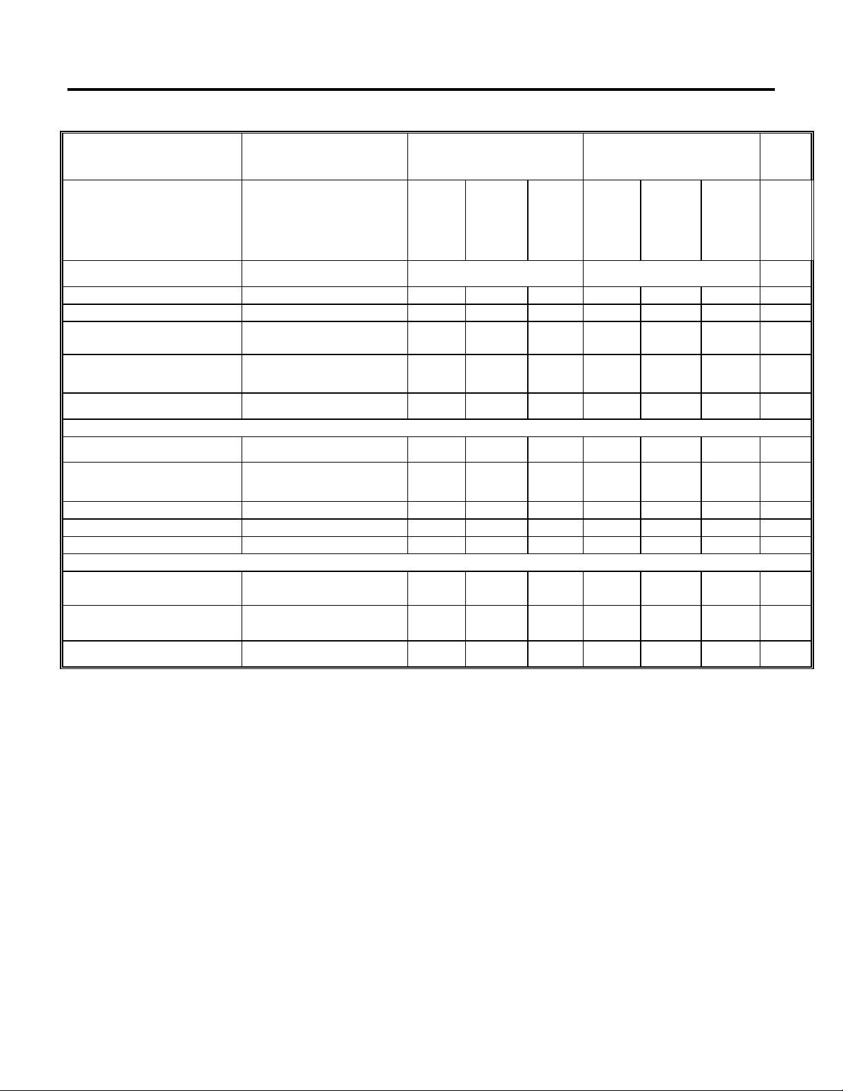
ELECTRICAL CHARACTERISTICS (Note 2) (Continued)
LP2950/LP2951
PARAMETER CONDITIONS
Output Noise,
10Hz to 100KHz
CL = 1µF
CL = 200 µF
CL = 13.3 µF
(Bypass = 0.01 µF pins 7 to
(Note 2)
LP2950AC
LP2951AC
Min. Typ. Max.
430
160
100
LP2950C
LP2951C
Min. Typ. Max.
430
160
100
Units
µV rms
µV rms
µV rms
1(LP2951))
8-Pin Versions only LP2951AC LP2951C
Reference Voltage 1.22 1.235 1.25 1.21 1.235 1.26 V
Reference Voltage Over Temperature (Note 7)
1.19 1.27 1.185 1.285
Feedback Pin Bias Current 40 60 40 60 nA
Reference Voltage Temperature
Coefficient
Feedback Pin Bias Current
Temperature Coefficient
( Note 12 )
20 50 ppm/°C
0.1 0.1 nA/°C
Error Comparator
Output Leakage Current
Output Low Voltage
V
= 30V 0.01 1 0.01 1
OH
Vin = 4.5V
150 250 150 250 mV
µA
IOL = 400µA
Upper Threshold Voltage
Lower Threshold Voltage
Hysteresis
(Note 6) 40 60 40 60 mV
(Note 6) 75 95 75 95 mV
(Note 6) 15 15 mV
Shutdown Input
Input logic Voltage
Shutdown Pin Input Current
(Note 3)
Regulator Output Current in
Shutdown (Note 3)
Low (Regulator ON)
High (Regulator OFF)
2
Vs = 2.4V
Vs = 30V
(Note 11) 3 10 3 10
1.3
30
450
0.7
50
600
1.3
0.7
2
30
450
50
600
µA
µA
µA
V
V
V
Note 1: Absolute Maximum Ratings are limits beyond which damage to the device may occur. Operating Ratings are conditions under which operation of the
device is guaranteed. Operating Ratings do not imply guaranteed performance limits. For guaranteed performance limits and associated test conditions, see the
Electrical Characteristics tables.
Note 2: Unless otherwise specified all limits guaranteed for V
IN
= ( V
+1)V, IL = 100 µA and CL = 1 µF for 5V versions and 2.2µF for 3V and 3.3V versions.
ONOM
Limits appearing in boldface type apply over the entire junction temperature range for operation. Limits appearing in normal type apply for TA = TJ = 25°C
Additional conditions for the 8-pin versions are FEEDBACK tied to V
, OUTPUT tied to SENSE and V
TAP
SHUTDOWN
≤ 0.8V.
Note 3: Guaranteed and 100% production tested.
Note 4: Guaranteed but not 100% production tested. These limits are not used to calculate outgoing AQL levels.
Note 5: Dropout voltage is defined as the input to output differential at which the output voltage drops 100 mV below its nominal value measured at 1V differential.
At very low values of programmed output voltage, the minimum input supply voltage of 2V ( 2.3V over temperature) must be taken into account.
Note 6: Comparator thresholds are expressed in terms of a voltage differential at the feedback terminal below the nominal reference voltage measured at
V
IN
= ( V
+1)V. To express these thresholds in terms of output voltage change, multiply by the error amplifier gain = Vout/Vref = (R1 + R2)/R2. For example,
ONOM
at a programmed output voltage of 5V, the error output is guaranteed to go low when the output drops by 95 mV x 5V/1.235 = 384 mV. Thresholds remain constant
as a percent of V
Note 7: V
as V
is varied, with the dropout warning occurring at typically 5% below nominal, 7.5% guaranteed.
out
out
≤ (Vin - 1V), 2.3 ≤Vin≤30V, 100µA≤IL≤ 100 mA, TJ ≤ T
ref ≤Vout
JMAX
.
Note 8: The junction-to-ambient thermal resistance are as follows:180°C/W and 160°C/W for the TO-92 (N) package with 0.40 inch and 0.25 inch leads to the
printed circuit board (PCB) respectively, 105°C/W for the molded plastic DIP (P) and 160°C/W for the molded plastic SO-8 (S). The above thermal resistances for
the N, S and P packages apply when the package is soldered directly to the PCB.
Note 9: May exceed input supply voltage.
Note 10: When used in dual-supply systems where the output terminal sees loads returned to a negative supply, the output voltage should be diode-clamped to
ground.
Note 11: V
≥ 2V, Vin ≤ 30V, V
shutdown
=0, Feedback pin tied to 5V
out
TAP
.
Note 12: Output or reference voltage temperature coefficients defined as the worst case voltage change divided by the total temperature range.
Advanced Monolithic Systems, Inc. 6680B Sierra Lane, Dublin, CA 94568 Phone (925) 556-9090 Fax (925) 556-9140
LP2950/LP2951
Note 13: Thermal regulation is defined as the change in output voltage at a time T after a change in power dissipation is applied, excluding load or line regulation
effects. Specifications are for a 50mA load pulse at VIN =30V (1.25W pulse) for T =10 ms.
Note 14: Regulation is measured at constant junction temperature, using pulse testing with a low duty cycle. Changes in output voltage due to heating effects are
covered under the specification for thermal regulation.
Note 15: Line regulation for the LP2951 is tested at 150°C for IL = 1 mA. For IL = 100 µA and TJ = 125°C, line regulation is guaranteed by design to 0.2%. See
typical performance characteristics for line regulation versus temperature and load current.
Note 16: All LP2950 devices have the nominal output voltage coded as the last two digits of the part number. In the LP2951 products, the 3.0V and 3.3V versions
are designated by the last two digits, but the 5V version is denoted with no code of the part number.
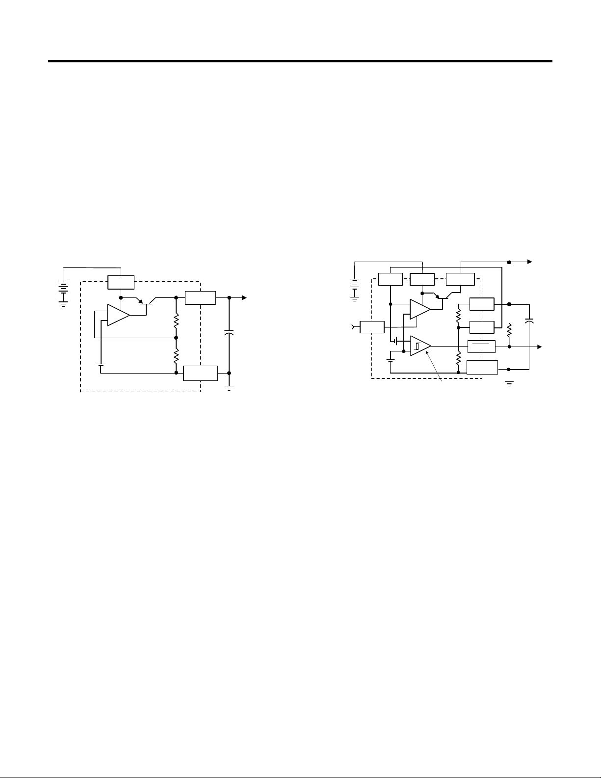
BLOCK DIAGRAM AND TYPICAL APPLICATIONS
LP2950-XX LP2951-XX
V
OUT
I
100mA
UNREGULATED DC
+
+
INPUT
+
ERROR
AMPLIFIER
1.23V
REFERENCE
OUTPUT
GROUND
V
IL≤ 100mA
+
SEE APPLICATION
OUT
HINTS
FROM
CMOS
OR TTL
UNREGULATED DC
+
FEEDBACK
+
+
-
+
+
-
1.23V
REFERENCE
3
SHUT-
DOWN
50mV
ERROR DETECTION COMPARATOR
INPUT OUTPUT
ERROR
AMPLIFIER
187
SENSE
ERROR
GROUND
≤
L
2
SEE APPLICATION
330k
+
Ω
TO CMOS
OR TTL
6
V
TAP
5
4
HINTS
Advanced Monolithic Systems, Inc. 6680B Sierra Lane, Dublin, CA 94568 Phone (925) 556-9090 Fax (925) 556-9140
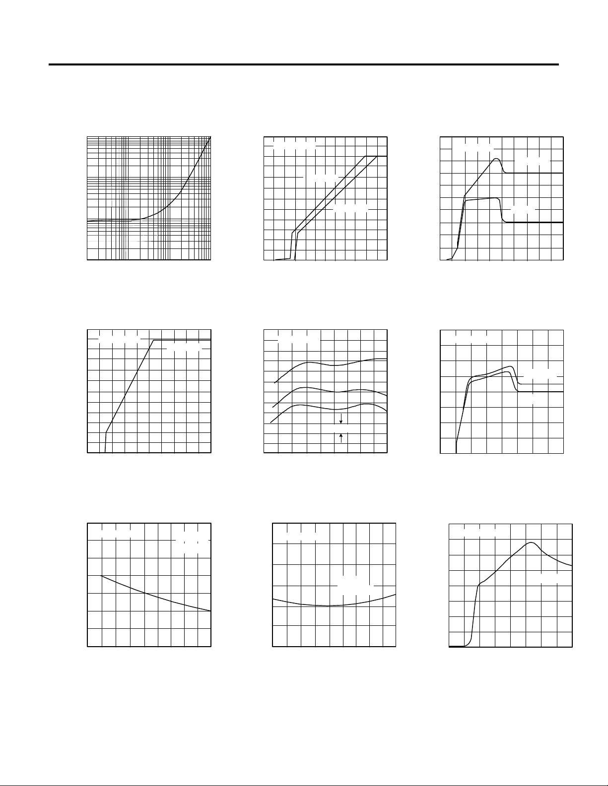
TYPICAL PERFORMANCE CHARACTERISTICS
LP2950/LP2951
Quiescent Current
10
1
0.1
GROUND CURRENT (mA)
0.01
0.1 1 10 100
LOAD CURRENT (mA)
Input Current
120
110
100
RL= 50Ω
90
80
70
60
50
40
30
INPUT CURRENT (mA)
20
10
0
1 2 3 4 5 6 7 8 9 100
INPUT VOLTAGE (V)
Dropout Characteristics
6
5V OUTPUT
5
4
RL= 50 kΩ
3
2
OUTPUT VOLTAGE (V)
1
0
1 2 3 4 5 6 1 2 3 4 5 6 7 8 9 100
0
INPUT VOLTAGE (V)
Temperature Drift of 3
Representative Units
5.06
5V OUTPUT5V OUTPUT 5V OUTPUT
5.04
5.02
5.0
4.98
OUTPUT VOLTAGE (V)
4.96
4.94
-75 0 25 50 75 100 125
-50 -25
TEMPERATURE (° C)
RL= 50Ω
0.2%
150
Input Current
250
225
5V OUTPUT
200
175
150
125
100
RL= ∞
75
INPUT CURRENT (µA)
50
25
0
INPUT VOLTAGE (V)
Quiescent Current
160
140
120
100
80
60
40
20
QUIESCENT CURRENT (µA)
0
0 1 2 3 4 5 6 7 8
INPUT VOLTAGE (V)
RL= 50 kΩ
IL= 1 mA
IL= 0
Quiescent Current
120
5V OUTPUT
110
A)
µ
100
90
80
70
60
QUIESCENT CURRENT (
50
-75
-50 -25
0 25 50 75 100 125
TEMPERATURE (° C)
IL= 100µA
VIN= 6V
150
Quiescent Current
5V OUTPUT
9
8
QUIESCENT CURRENT (mA)
7
-50 -25
-75
0 25 50 75 100 12510150
TEMPERATURE (° C)
VIN= 6V
IL= 100mA
Quiescent Current
8
5V OUTPUT
7
6
5
4
3
2
1
QUIESCENT CURRENT (µA)
0
0 1 2 3 4 5 6 7 8
INPUT VOLTAGE (V)
IL= 100mA
Advanced Monolithic Systems, Inc. 6680B Sierra Lane, Dublin, CA 94568 Phone (925) 556-9090 Fax (925) 556-9140
 Loading...