

ADVANCED Monolithic System AMS3102 Service Manual
Advanced AMS3102
Monolithic 300mA LOW DROPOUT VOLTAGE REGULATOR
Systems
FEATURES APPLICATIONS
•• Fixed and Adjustable Versions Available •• Cellular Telephones
•• Output Current in excess of 300mA •• Portable Consumer Equipment
•• Very Low Quiescent Current •• Portable (Notebook) Computers
•• Reverse Battery Protection •• Battery Powered Systems
•• Input-output Differential less than 0.6V •• Portable Instrumentation
•• Short Circuit Protection •• Radio Control Systems
•• Internal Thermal Overload Protection •• CD/DVD drives
•• Load Dump Protection
•• Overvoltage Protection
•• Mirror Image Insertion Protection
•• ON/OFF Pin
••External PNP Drive
GENERAL DESCRIPTION
The AMS3102 series consists of positive fixed and adjustable voltage regulators ideally suited for use in battery-powered
systems. These devices feature very low quiescent current of 0.3mA or less when supplying 10mA loads. This unique
characteristic and the extremely low input-output differential required for proper regulation (0.25V for output currents of
100mA) make the AMS3102 ideal to use for standby power systems.
Internal circuitry of AMS3102 is protected from input fault conditions caused by reverse battery installation or input voltages
that exceed maximum rated input voltage. During line transients, such as load dump (40V) when the input voltage to the
regulator can momentarily exceed the specified maximum operating voltage, the regulator will automatically shut down to
protect both internal circuits and the load. The AMS3102 series also includes internal current limiting, thermal shutdown,
and is able to withstand temporary power-up with mirror-image insertion.
The AMS3102 is offered in the 3-pin TO-92 package, SOT-89, 3 lead SOT-23, 5 lead SOT-23 and 8 lead SOIC packages.
The device is provided with On/Off pin in SOT-23 5L and in 8 lead SOIC package.
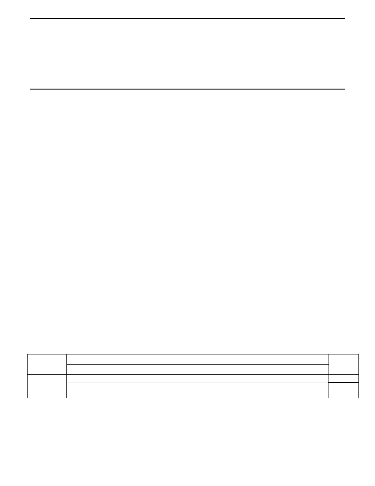
ORDERING INFORMATION
OUTPUT PACKAGE TYPE TEMP.
VOLTAGE
FIXED AMS3102AN-X AMS3102AL-X (R) AMS3102AM-X AMS3102AM1-X AMS3102AS-X IND
ADJ. AMS3102CM1 AMS3102CS IND
X = 2.0V, 2.5V, 3.0V, 3.3V, 3.5V, 4.0V, 5.0V.
R = Reverse pin-out option
TO-92 SOT-89 3L SOT-23 5L SOT-23 SO-8
AMS3102N-X AMS3102L-X (R) AMS3102M-X AMS3102M1-X AMS3102S-X IND
RANGE
Advanced Monolithic Systems, Inc. 6680B Sierra Lane, Dublin, CA 94568 Phone (925) 556-9090 Fax (925) 556-9140
AMS3102
ABSOLUTE MAXIMUM RATINGS (Note 1)
Input Voltage Maximum Junction Temperature
Operating 21V Storage Temperature
-65°C to +150°C
Overvoltage Protection 24V to 40V Lead Temperature (Soldering 10 sec)
Internal Power Dissipation (Note 4) Internally Limited ESD 2000V
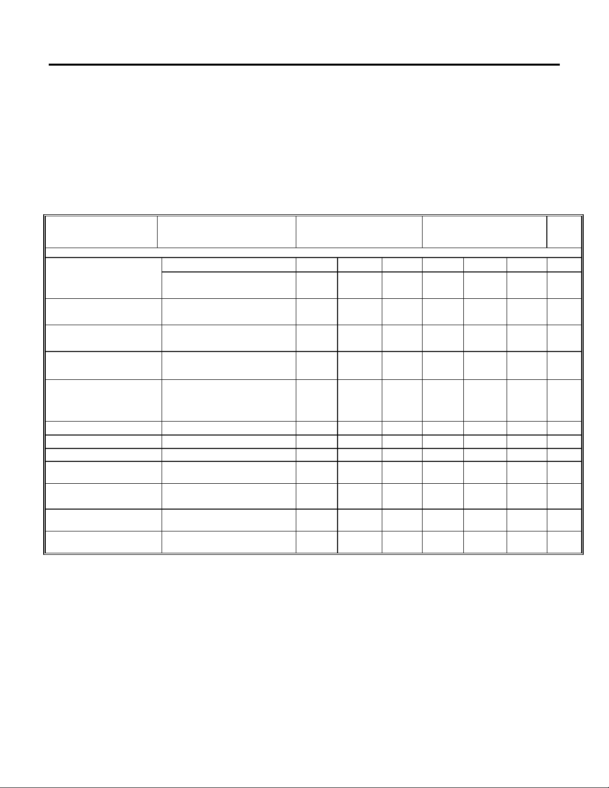
ELECTRICAL CHARACTERISTICS
Electrical Characteristics at V
+1V, IO =10mA, TJ=25°C, C2 = 22µF unless otherwise specified.
IN =VO
+125°C
230°C
PARAMETER CONDITIONS
AMS3102A-X
Min. Typ. Max.
Fixed Output Voltage Versions
Output Voltage Tolerance -1.0 +1.0 -3.0 +3.0 %
(VIN+1V) ≤VIN ≤21V, IO=100 mA
-40°C ≤T
Line Regulation
Load Regulation
Dropout Voltage I
Quiescent Current
Output Noise Voltage
Output Impedance 100mADC and 10mA
Ripple Rejection fO =120Hz 55 80 80 dB
Maximum Operational Input
Voltage
Maximum Line Transient
Reverse Polarity Input Voltage,
D/C
Reverse Polarity Input Voltage,
Transient
(VIN+1V) ≤VIN ≤ 15V
9V ≤VIN ≤ 21V
5mA ≤I
5mA ≤10 ≤ 200 mA
O
I
O
I
O
I
O
I
O
10Hz-100kHz, C
RL = 500Ω, VO ≤ 5.5V
T = 1ms, τ ≤100ms
RL = 500Ω, T = 1ms, τ ≤100ms
≤125°C
J
≤ 100 mA
O
= 100 mA
= 200 mA
≤ 10 mA,
= 100 mA
≤ 200 mA (Note 5)
OUT
= 100µF
,100Hz=10kHz 200 200
rms
- 3.0 + 3.0
5
8
30
50
0.25
0.5
0.3
3
9
500 500
21 22 21 22 V
35 40 35 40 V
-35 -40 -35 -40 V
-35 -40 -35 -40 V
10
30
50
70
0.3
0.6
0.5
4
12
AMS3102-X
Min. Typ. Max.
±± 5.0
5
8
30
50
0.3
0.5
0.3
3
9
10
30
50
70
0.4
0.6
0.5
4
12
Units
%
mV
mV
mV
mV
mV
mV
mA
mA
mA
µV rms
mΩ
Advanced Monolithic Systems, Inc. 6680B Sierra Lane, Dublin, CA 94568 Phone (925) 556-9090 Fax (925) 556-9140
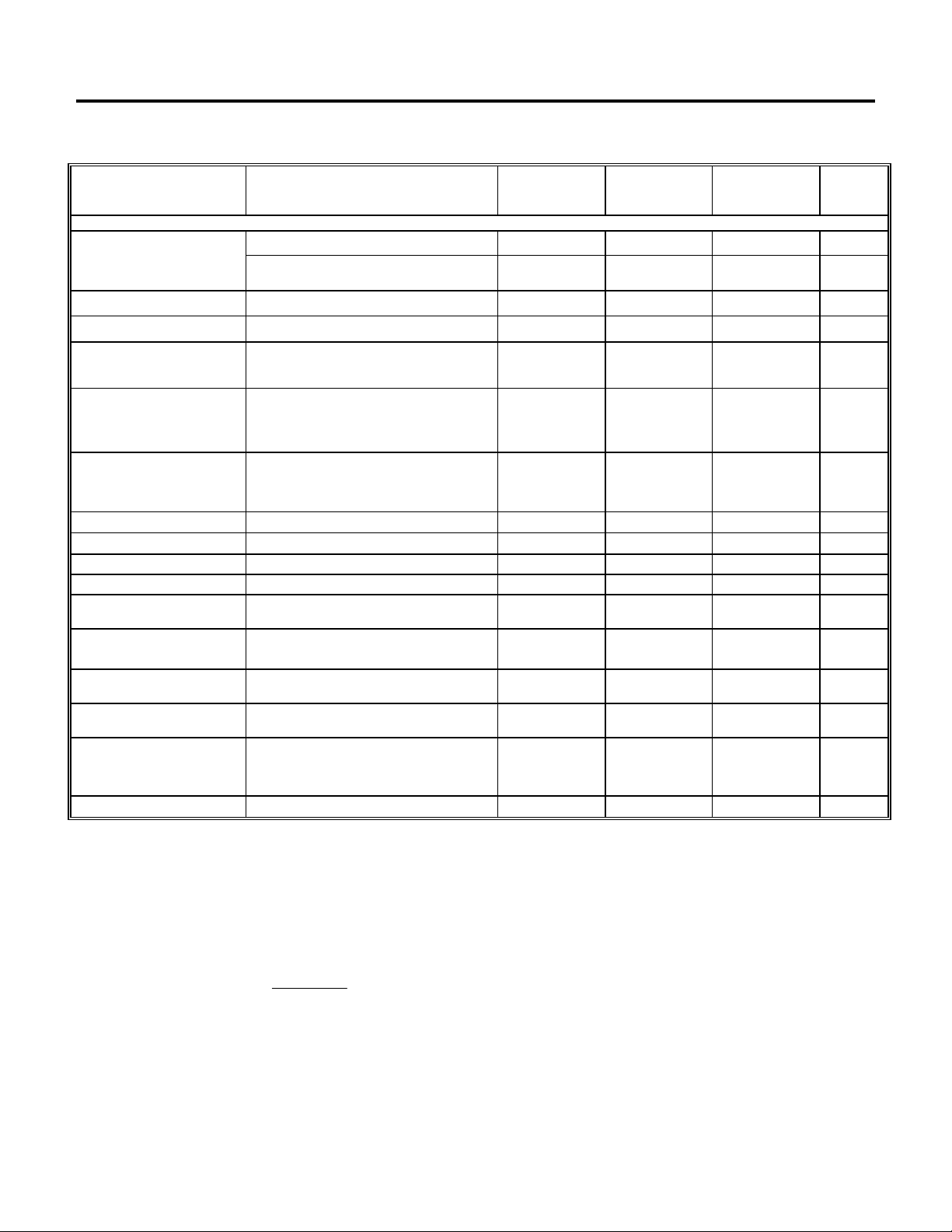
ELECTRICAL CHARACTERISTICS
Electrical Characteristics at V
=6V, V
IN
=3V IO =10mA, TJ=25°C, R1 =27k, C2 = 2µF unless otherwise specified.
OUT
AMS3102
PARAMETER CONDITIONS
(Note 2)
Min.
AMS3102C
Typ.
Max.
Units
Adjustable Version
Reference Voltage
IO ≤ 100 mA, -40°C ≤T
Measured from V
to Adjust Pin
OUT
≤ 125°C, R1=27k,
J
1.210 1.235 1.26 V
1.20 1.235 1.270
V
Output Voltage Range 2 20 V
Line Regulation
Load Regulation
V
+ 1V ≤VIN ≤ 21V
OUT
5mA ≤IO ≤ 100 mA
5mA ≤IO ≤ 200 mA
Dropout Voltage
Quiescent Current I
I
≤ 10 mA
O
I
= 100 mA
O
I
= 200 mA (Note 5)
O
= 10 mA
O
I
= 100 mA
O
During Shutdown RL = 500Ω
Output Noise Voltage 10Hz-100kHz 100
Output Impedance 100mADC and 10mA
,100Hz=10kHz 40 200
rms
.02 1.5 mV/V
0.3
1
0.05
0.3
0.5
0.3
3
0.3
0.2
0.4
0.6
0.5
0.5
1
2
%
%
V
V
V
mA
4
mA
mA
µV
rms
mΩ
/V
Long Term Stability T =1000hr 0.4 %/1000hr
Ripple Rejection fO = 120Hz 0.02 dB
Maximum Operational Input
21 22 V
Voltage
Maximum Line Transient
IO = 10mA, Reference Voltage ≤ 1.5V
35 40 V
T = 1ms, τ ≤100ms
Reverse Polarity Input Voltage,
RL = 500Ω, VO ≥ -0.3V
-35 -40 V
D/C
Reverse Polarity Input Voltage,
RL = 500Ω, T = 1ms, τ ≤100ms
-35 -40 V
Transient
On/Off Threshold Voltage
On
Off
On/Off Threshold Current V
VO = 3V
1.8
2.5
= 2.4V 35 60
OFF
2.0
1.5 V
V
µA
Note 1: Absolute Maximum Ratings are limits beyond which damage to the device may occur. For guaranteed performance limits and associated test conditions, see
the Electrical Characteristics tables.
Note 2: To ensure constant junction temperature, low duty cycle pulse testing is used.
Note 3: Limits appearing in boldface type apply over the entire junction temperature range for operation. Limits appearing in normal type apply for
TA = TJ = 25°C.
Note 4: The maximum allowable power dissipation is a function of the maximum junction temperature TJ(MAX), the junction-to ambient thermal resistance θ
J-A
the ambient temperature TA. The maximum allowable power dissipation at any ambient temperature is calculated using:
P(MAX)θ=
AJ T-(MAX)T
A-J
Where the value of the junction-to-ambient thermal resistance are as follows: 195°C/W for the TO-92 (N) package, 110°C/W for SOT-89 (L), 220°C/W for 5 lead
SOT-23 (M1) and 160°C/W for the molded plastic SO-8 (S).
Note 5: Dropout Voltage is defined as the input to output differential at which the output voltage drops 100mV below its nominal value measured at 1V differential.
Advanced Monolithic Systems, Inc. 6680B Sierra Lane, Dublin, CA 94568 Phone (925) 556-9090 Fax (925) 556-9140
and
 Loading...