

ADVANCED Monolithic System AMS1117 Service Manual
g
查询AMS1117_05供应商
Advanced AMS1117
Monolithic 1A LOW DROPOUT VOLTAGE REGULATOR
Systems
RoHS compliant
FEATURES APPLICATIONS
• Three Terminal Adjustable or Fixed Voltages* • High Efficiency Linear Regulators
1.5V, 1.8V, 2.5V, 2.85V, 3.3V and 5.0V
• Post Re
• Output Current of 1A • 5V to 3.3V Linear Regulator
• Operates Down to 1V Dropout • Battery Chargers
• Line Regulation: 0.2% Max. • Active SCSI Terminators
• Load Regulation: 0.4% Max. • Power Management for Notebook
• SOT-223, TO-252 and SO-8 package available • Battery Powered Instrumentation
GENERAL DESCRIPTION
The AMS1117 series of adjustable and fixed voltage regulators are designed to provide 1A output current and to operate
down to 1V input-to-output differential. The dropout voltage of the device is guaranteed maximum 1.3V at maximum output
current, decreasing at lower load currents.
On-chip trimming adjusts the reference voltage to 1%. Current limit is also trimmed, minimizing the stress under overload
conditions on both the regulator and power source circuitry.
The AMS1117 devices are pin compatible with other three-terminal SCSI regulators and are offered in the low profile surface
mount SOT-223 package, in the 8L SOIC package and in the TO-252 (DPAK) plastic package.
ORDERING INFORMATION:
TO-252 SOT-223 8L SOIC
AMS1117CD AMS1117 AMS1117CS
AMS1117CD-1.5 AMS1117-1.5 AMS1117CS-1.5
AMS1117CD-1.8 AMS1117-1.8 AMS1117CS-1.8
AMS1117CD-2.5 AMS1117-2.5 AMS1117CS-2.5
AMS1117CD-2.85 AMS1117-2.85 AMS1117CS-2.85
AMS1117CD-3.3 AMS1117-3.3 AMS1117CS-3.3
AMS1117CD-5.0 AMS1117-5.0 AMS1117CS-5.0
PACKAGE TYPE OPERATING JUNCTION
TEMPERATURE RANGE
-40 to 125° C
-40 to 125° C
-40 to 125° C
-40 to 125° C
-40 to 125° C
-40 to 125° C
-40 to 125° C
*For additional available fixed voltages contact factory.
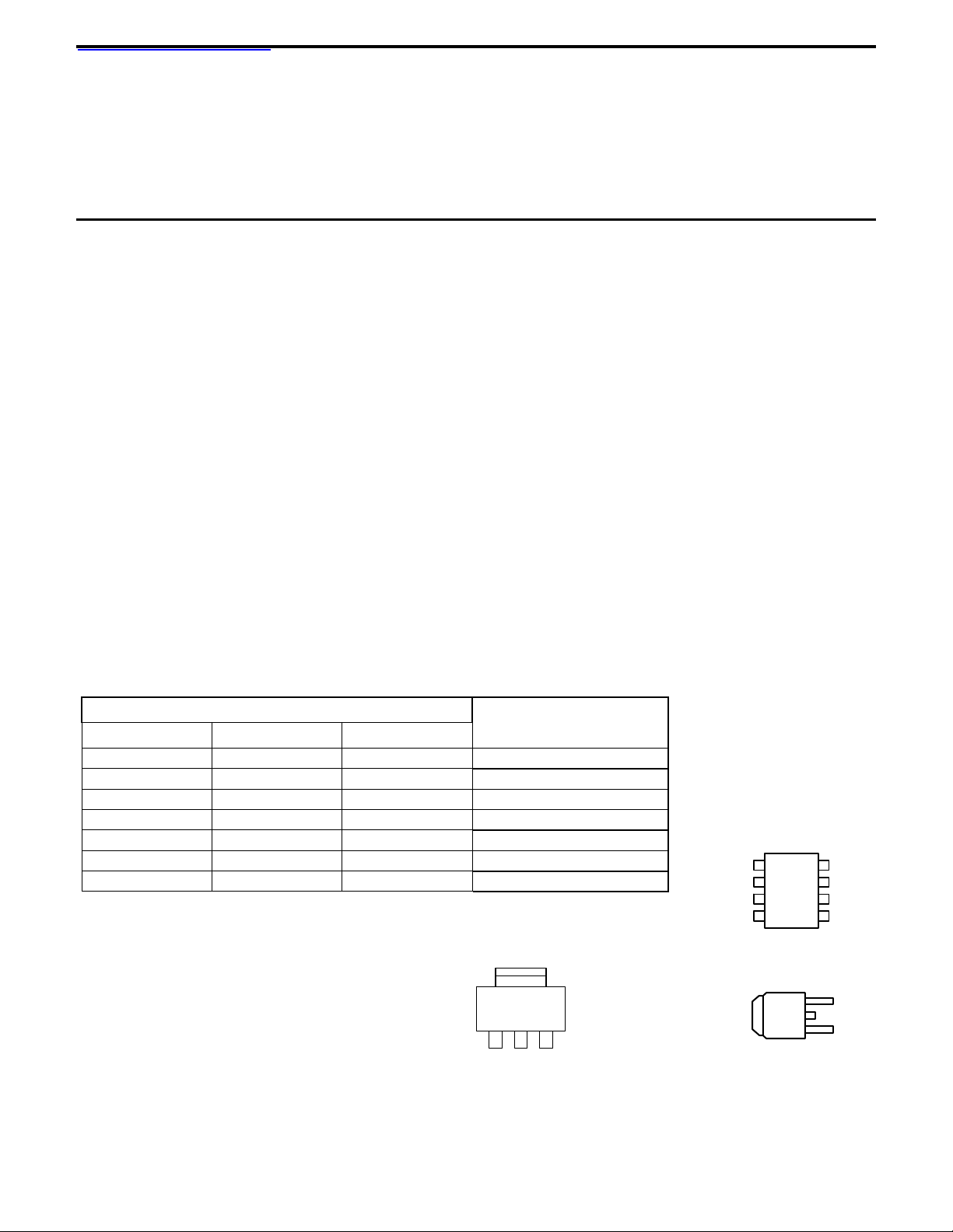
PIN CONNECTIONS
SOT-223 Top View
3 PIN FIXED/ADJUSTABLE
VERSION
1- Ground/Adjust
2- V
OUT
3- V
IN
1
2
3
ulators for Switching Supplies
8L SOIC Top View
GND/ADJ
V
OUT
V
OUT
V
IN
1
2
3
4
TO-252 FRONT VIEW
TAB IS
OUTPUT
3
2
1
8
N/C
7
V
OUT
6
V
OUT
5
N/C
Advanced Monolithic Systems, Inc. www.advanced-monolithic.com Phone (925) 443-0722 Fax (925) 443-0723
AMS1117
ABSOLUTE MAXIMUM RATINGS (Note 1)
Power Dissipation Internally limited Soldering information
Input Voltage 15V Lead Temperature (25 sec)
Operating Junction Temperature Thermal Resistance
Control Section
Power Transistor
Storage temperature
0°C to 125°C
0°C to 150°C
- 65°C to +150°C
SO-8 package
TO-252 package
SOT-223 package
* With package soldering to copper area over backside
ground plane or internal power plane ϕ
46°C/W to >90°C/W depending on mounting technique and
the size of the copper area.
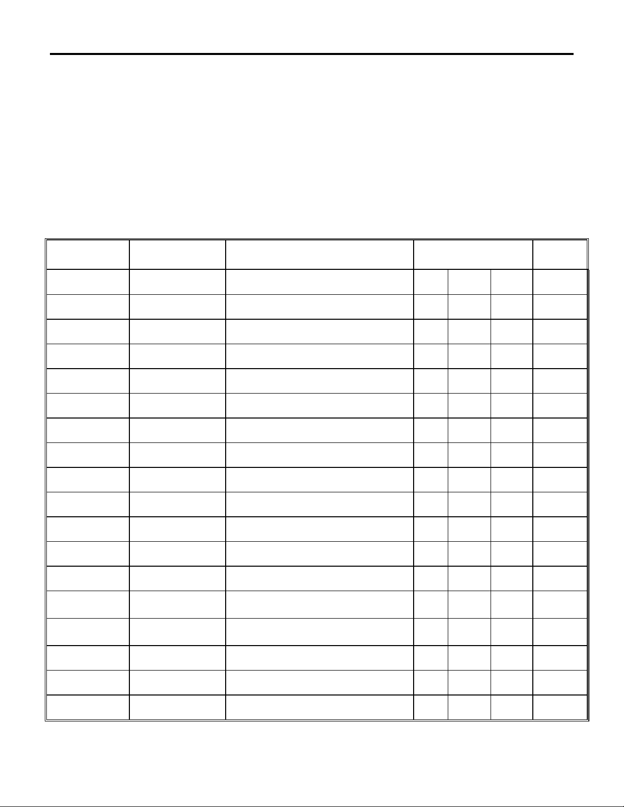
ELECTRICAL CHARACTERISTICS
Electrical Characteristics at I
= 0 mA, and TJ = +25°C unless otherwise specified.
OUT
265°C
= 160°C/W
ϕ
JA
= 80°C/W
ϕ
JA
= 90°C/W*
ϕ
JA
can vary from
JA
Parameter
Device Conditions Min Typ Max Units
Reference Voltage
(Note 2)
Output Voltage
(Note 2)
Line Regulation AMS1117
AMS1117-1.5
AMS1117-1.8
AMS1117-2.5
AMS1117-2.85
AMS1117-3.3
AMS1117-5.0
Load Regulation
(Notes 2, 3)
AMS1117-1.5
AMS1117-1.8
AMS1117-2.5
AMS1117 I
AMS1117-1.5
AMS1117-1.8
AMS1117-2.5
AMS1117-2.85
AMS1117-3.3
AMS1117-5.0
AMS1117
= 10 mA
OUT
10mA ≤ I
≤ 1A , 3.0V≤ VIN ≤ 12V
0 ≤ I
OUT
≤ 1A , 3.3V≤ VIN ≤ 12V
0 ≤ I
OUT
≤ 1A , 4.0V≤ VIN ≤ 12V
0 ≤ I
OUT
≤ 1A , 4.35V≤ VIN ≤ 12V
0 ≤ I
OUT
≤ 1A , 4.75V ≤ VIN ≤ 12V
0 ≤ I
OUT
≤ 1A , 6.5V ≤ VIN ≤ 12V
0 ≤ I
OUT
= 10 mA , 1.5V≤ (VIN - V
I
LOAD
3.0V≤ V
IN
3.3V≤ V
IN
4.0V≤ V
IN
4.35V≤ V
4.75V≤ V
6.5V≤ V
IN
- V
(V
IN
OUT
= 5V, 0 ≤ I
V
IN
= 5V, 0 ≤ I
V
IN
= 5V, 0 ≤ I
V
IN
≤ 1A, 1.5V≤ (VIN - V
OUT
≤ 12V
≤ 12V
≤ 12V
≤ 12V
IN
≤ 12V
IN
≤ 12V
) =3V, 10mA ≤ I
≤ 1A
OUT
≤ 1A
OUT
≤ 1A
OUT
OUT
OUT
) ≤ 12V
OUT
≤ 1A
) ≤ 12V
1.238
1.225
1.485
1.476
1.782
1.773
2.475
2.460
2.82
2.79
3.267
3.235
4.950
4.900
1.250
1.250
1.500
1.500
1.800
1.800
2.500
2.500
2.850
2.850
3.300
3.300
5.000
5.000
0.015
0.035
0.3
0.3
0.3
0.3
0.5
0.5
3 6 10
3 6 10
3 6 12
0.6
0.6
0.6
0.6
1.0
1.0
0.1
0.2
1.262
1.270
1.515
1.524
1.818
1.827
2.525
2.560
2.88
2.91
3.333
3.365
5.050
5.100
0.2
0.2
5
6
5
6
6
6
6
6
10
10
10
10
0.3
0.4
20
20
20
V
V
V
V
V
V
V
V
V
V
V
V
V
V
%
%
mV
mV
mV
mV
mV
mV
mV
mV
mV
mV
mV
mV
%
%
mV
mV
mV
mV
mV
mV
Advanced Monolithic Systems, Inc. www.advanced-monolithic.com Phone (925) 443-0722 Fax (925) 443-0723
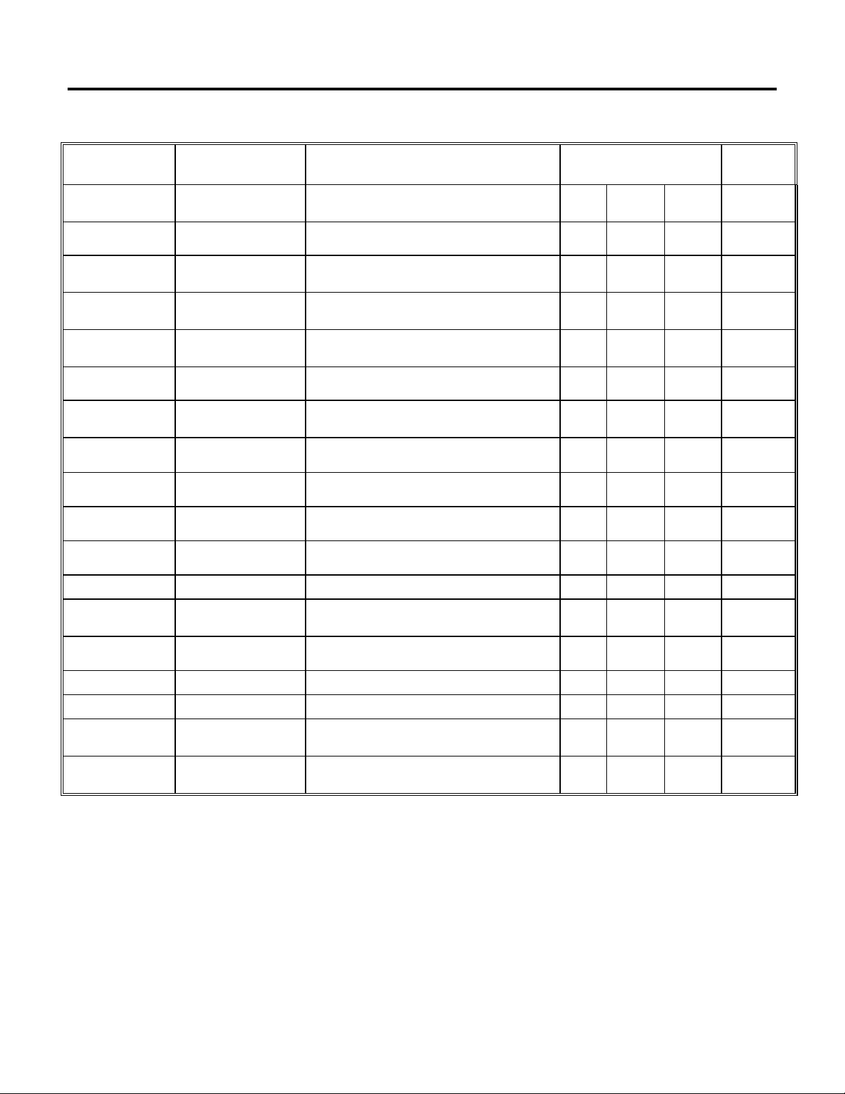
ELECTRICAL CHARACTERISTICS
Electrical Characteristics at I
= 0 mA, and TJ = +25°C unless otherwise specified.
OUT
AMS1117
Parameter
Device Conditions Min Typ Max Units
Load Regulation
AMS1117-2.85
= 5V, 0 ≤ I
V
IN
(Notes 2, 3)
AMS1117-3.3
= 5V, 0 ≤ I
V
IN
OUT
OUT
≤ 1A
≤ 1A
3 6 12
20
3 7 15
25
AMS1117-5.0
Dropout Voltage
- V
OUT
)
(V
IN
Current Limit
Minimum Load
AMS1117-1.5/-1.8/-2.5/-
2.85/-3.3/-5.0
AMS1117-1.5/-1.8/-2.5/-
2.85/-3.3/-5.0
AMS1117 (VIN - V
= 8V, 0 ≤ I
V
IN
∆V
OUT
(VIN - V
, ∆V
≤ 1A
OUT
= 1%, I
REF
) = 5V
OUT
) = 12V (Note 5)
OUT
= 1A (Note 4)
OUT
5
10
1.1 1.3
900 1,100 1,500
5 10
20
35
Current
≤ 12V
V
Quiescent Current AMS1117-1.5/-1.8/-2.5/-
IN
2.85/-3.3/-5.0
Ripple Rejection AMS1117
AMS1117-1.5/-1.8/-2.5/-
2.85
AMS1117-3.3
AMS1117-5.0
f =120Hz , C
(V
IN-VOUT
f =120Hz , C
= 6V
V
IN
f =120Hz , C
= 6.3V
V
IN
f =120Hz , C
= 8V
V
IN
= 22µF Tantalum, I
OUT
) = 3V, C
ADJ
= 22µF Tantalum, I
OUT
= 22µF Tantalum, I
OUT
= 22µF Tantalum, I
OUT
=10µF
OUT
OUT
OUT
OUT
= 1A,
= 1A,
= 1A
= 1A
5
60 75
60
72
60 72
60 68
dB
10
Thermal Regulation AMS1117 TA = 25°C, 30ms pulse 0.008 0.04 %W
mV
mV
mV
mV
mV
mV
V
mA
mA
mA
dB
dB
dB
Adjust Pin Current AMS1117
Adjust Pin Current
AMS1117
Change
Temperature Stability
10mA ≤ I
10mA ≤ I
≤ 1A , 1.5V≤ (VIN - V
OUT
≤ 1A , 1.5V≤ (VIN - V
OUT
OUT
OUT
) ≤ 12V
) ≤ 12V
55
0.2
0.5
120
5
µA
µA
µA
%
Long Term Stability TA =125°C, 1000Hrs 0.3 1 %
RMS Output Noise
OUT
)
(% of V
Thermal Resistance
= 25°C , 10Hz ≤ f ≤ 10kHz
T
A
0.003 %
15 °C/W
Junction-to-Case
Parameters identified with boldface type apply over the full operating temperature range.
Note 1: Absolute Maximum Ratings indicate limits beyond which damage to the device may occur. For guaranteed specifications and test conditions, see the
Electrical Characteristics
. The guaranteed specifications apply only for the test conditions listed.
Note 2: Line and Load regulation are guaranteed up to the maximum power dissipation of 1.2 W. Power dissipation is determined by the input/output
differential and the output current. Guaranteed maximum power dissipation will not be available over the full input/output range.
Note 3: See thermal regulation specifications for changes in output voltage due to heating effects. Line and load regulation are measured at a constant junction
temperature by low duty cycle pulse testing. Load regulation is measured at the output lead ~1/8” from the package.
Note 4: Dropout voltage is specified over the full output current range of the device.
Note 5: Minimum load current is defined as the minimum output current required to maintain regulation. When 1.5V ≤ (V
guaranteed to regulate if the output current is greater than 10mA.
- V
) ≤ 12V the device is
IN
OUT
Advanced Monolithic Systems, Inc. www.advanced-monolithic.com Phone (925) 443-0722 Fax (925) 443-0723
 Loading...