

Advanced Linear Devices Inc ALD1110ESC, ALD1110ESA, ALD1110EPC, ALD1110EPA Datasheet
FEATURES
•
Operates from 2V, 3V, 5V to 10V
•
Flexible basic circuit building block and design element
•
Very high resolution -- average programmable voltage
resolution of 0.1mV
•
Wide dynamic range -- current levels from 0.1µA
to 3000µA
•
Voltage adjustment range from 1.000V to 3.000V
in 0.1mV steps
•
Proven, non-volatile CMOS technology
•
Typical 10 years drift of less than 2mV
•
Usable in voltage mode or current mode
•
High input impedance -- 1012Ω
•
Very high DC current gain -- greater than 10
9
•
Device operating current has positive temperature
coefficient range and negative temperature
coefficient range with cross-over zero temperature
coefficient current level at 68µA
•
Tight matching and tracking of on-resistance
between different devices with programming
•
Very low input currents and leakage currents
•
Low cost, monolithic technology
•
Application-specific or in-system programming modes
•
User programmable software-controlled automation
•
User programmability of any standard/custom
configuration
•
Micropower operation
•
Available in standard PDIP, SOIC and hermetic
CDIP packages
•
Suitable for matched-pair balanced circuit configuration
•
Suitable for both coarse and fine trimming applications
QUAD/DUAL ELECTRICALLY PROGRAMMABLE ANALOG DEVICE (EPAD™)
ADVANCED
LINEAR
DEVICES, INC.
ALD1108E/ALD1110E
BENEFITS
•
Simple, elegant single-chip solution
to trimming voltage/current values
•
Direct in-circuit active element operation
and programming
•
Remotely and electrically trim parameters on
circuits that are physically inaccessible
•
Usable in environmentally sealed circuits
•
No system overhead or active circuitry required
•
No mechanical moving parts -- high G-shock
tolerance
•
Improved reliability, dependability, dust and
moisture resistance
•
Cost and labor savings
•
Small footprint for high board density
applications
•
Fully automated test and trimming environment
Operating Temperature Range*
-55°C to +125°C0°C to +70°C0°C to +70°C
8-Pin 8-Pin 8-Pin
CERDIP Plastic Dip SOIC
Package Package Package
ALD1110E DA ALD1110E PA ALD1110E SA
Operating Temperature Range*
-55°C to +125°C0°C to +70°C0°C to +70°C
16-Pin 16-Pin 16-Pin
CERDIP Plastic Dip SOIC
Package Package Package
ALD1108E DC ALD1108E PC ALD1108E SC
ORDERING INFORMATION
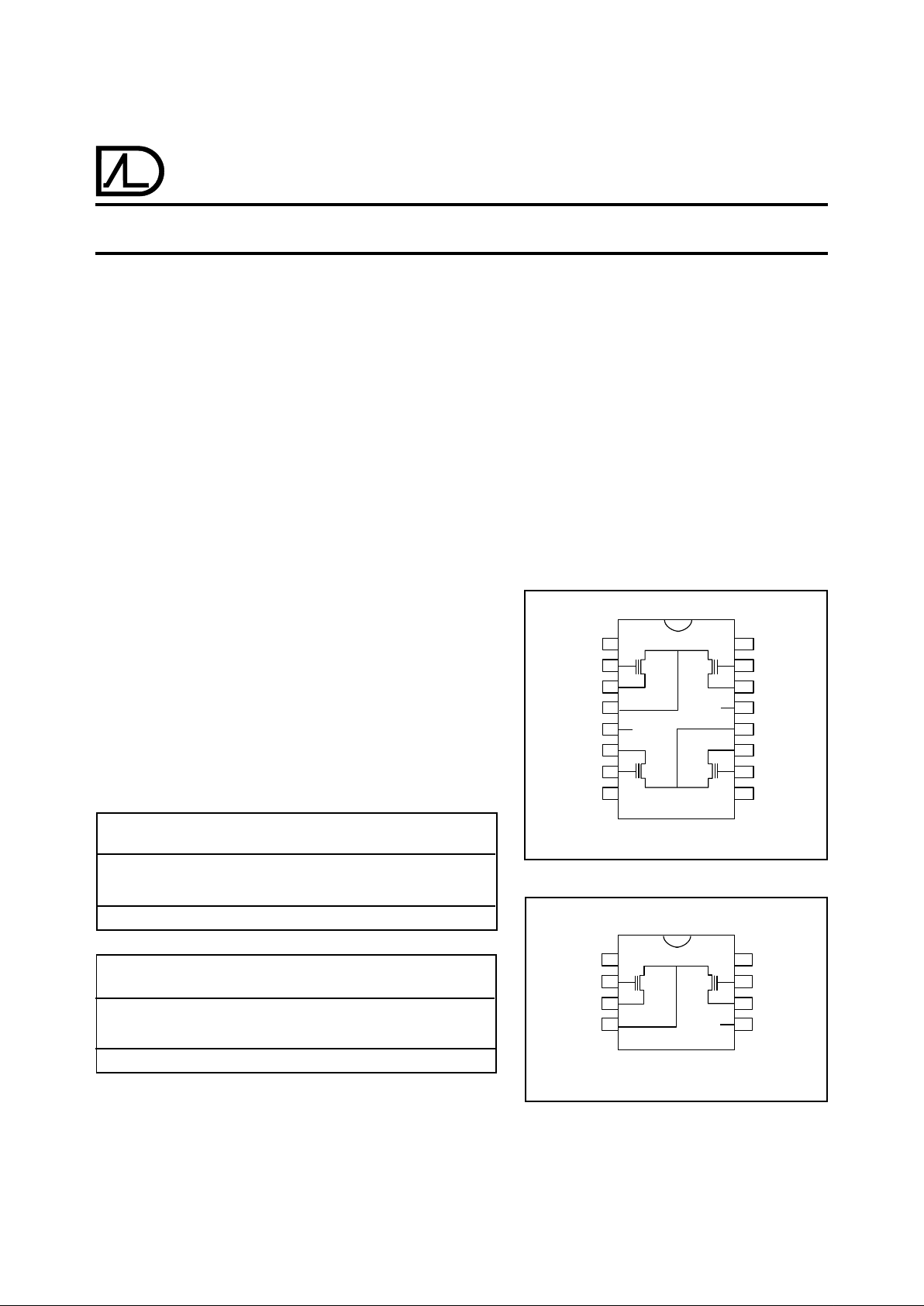
PIN CONFIGURATION
PIN CONFIGURATION
* Contact factory for industrial temperature range
P
N2
1
2
3
14
15
16
4
13
V
+
5
12
S
34
P
N3
6
7
8
10
11
G
N1
D
N1
P
N1
S
12
V
-
G
N4
P
N4
D
N4
9
G
N3
D
N3
D
N2
G
N2
DC, PC, SC PACKAGE
v
-
v
+
ALD1108E
EPAD 1
EPAD 2
EPAD 4
EPAD 3
P
N2
1
2
3
6
7
8
4
5
V
+
G
N1
D
N1
P
N1
S12, V
-
D
N2
G
N2
DA, PA, SA PACKAGE
v
+
ALD1110E
EPAD 1
EPAD 2
© 1998 Advanced Linear Devices , Inc. 415 T asman Dr ive, Sunn yvale, Calif ornia 94089 -1706 T el: (408) 747-1155 F ax: (408) 747-1286 http://www.aldinc.com
ALD1108E/ALD1110E Advanced Linear Devices 2
GENERAL DESCRIPTION
ALD1108E/ALD1110E are monolithic quad/dual EPADs (Electrically
Programmable Analog Device) that utilize CMOS MOSFET with electrically programmable threshold voltage. For a given input voltage,
changing the threshold turn-on voltage of a MOSFET device precisely
changes its drain on-current, resulting in an on-resistance characteristic that can be precisely set and controlled. Used as an in-circuit element
for trimming or setting a combination of voltage and/or current characteristics, it can be programmed via a Personal Computer remotely and
automatically via software control. Once programmed and set, the set
voltage and current levels are stored indefinitely inside the device as a
precisely controlled nonvolatile stored charge, which is not affected
during normal operation of the device, even after power has been turned
off.
The ALD1108E/ALD1110E are devices built with ALD's EPAD technology, an electrically programmable device technology refined for analog
applications. The ALD1108E/ALD1110E functions like a regular MOSFET
transistor except with precise user preset threshold voltage. Using the
ALD1108E/ALD1110E is simple and straight forward. The device is
extremely versatile as a circuit element and design component. It
presents the user with a wealth of possible applications, limited only by
the imagination of the user and the many ways an analog MOSFET
device can be used as a circuit design element. The ALD1108E/
ALD1110E do not need other active circuitry for functionality.
The basic device is a monotonically adjustable device which means the
device can normally be programmed to increase in threshold voltage
and to decrease in drain-on current as a function of a given input bias
voltage. Once adjusted, the voltage and current conditions are permanent and not reversible. However, a given EPAD device can be adjusted
many times to continually increase the threshold voltage. A pair of EPAD
devices can also be connected such that one device is used to adjust a
parameter in one direction and the other device is used to adjust the
same parameter in the other direction.
The ALD1108E/ALD1110E can be pre-programmed with the ALD
EPAD programmer to obtain the desired voltage and current levels. Or,
they can be programmed as an active in-system element in a user
system, via user designed interface circuitry. For more information, see
Application Note AN1108.
APPLICATIONS
•
Precision PC-based electronic calibration
•
Automated voltage trimming or setting
•
Remote voltage or current adjustment of
inaccessible nodes
•
PCMCIA based instrumentation trimming
•
Electrically adjusted resistive load
•
Temperature compensated current sources
and current mirrors
•
Electrically trimmed/calibrated current
sources
•
Permanent precision preset voltage level
shifter
•
Low temperature coefficient voltage and/or
current bias circuits
•
Multiple preset voltage bias circuits
•
Multiple channel resistor pull-up or pull-down
circuits
•
Microprocessor based process control systems
•
Portable data acquisition systems
•
Battery operated terminals and instruments
•
Remote telemetry systems
•
Programmable gain amplifiers
•
Low level signal conditioning
•
Sensor and transducer bias currents
•
Neural networks
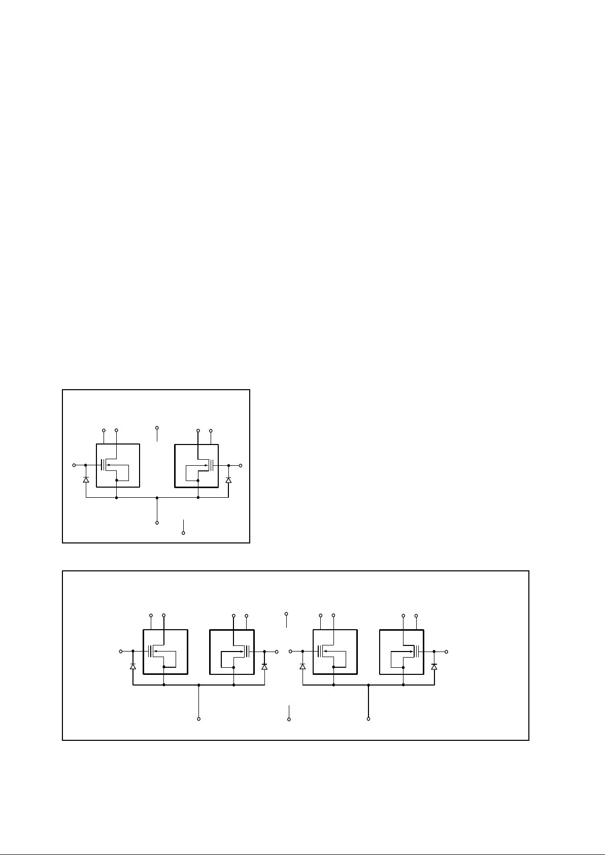
BLOCK DIAGRAM
P
N1
(1) DN1 (3)
G
N1
(2)
D
N2
(6)
P
N2
(8)
G
N2
(7
)
V- (4)
V+(5)
S
12
(4)
ALD1110E
EPAD 1
EPAD 2
~
~
BLOCK DIAGRAM
EPAD 1
EPAD 2 EPAD 3 EPAD 4
PN4 (8)
P
N
(1) DN1 (3)
G
N1
(2)
D
N2
(14)
P
N2
(16)
G
N2
(15)
P
N3
(9)
D
N3
(11)
G
N3
(10)
D
N4
(6)
G
N4
(7)
V- (5)
V+(13)
S
12
(4) S34 (12)
ALD1108E
~
~

ALD1108E/ALD1110E Advanced Linear Devices 3
Supply Voltage V
+
1.2 10.0 1.2 10.0 V
Initial Threshold Voltage V
ti
0.990 1.000 1.010 0.990 1.000 1.010 V IDS = 1µA TA = 21°C
Programmable Vt Range V
t 1.000
3.000 1.000 3.000 V
Drain - Gate Connected TCV
DS
-1.6 -1.6 mV/°CI
D
= 5µA
Voltage Tempco -0.3 -0.3 mV/°CI
D
= 50µA
0.0 0.0 mV/°CI
D
= 68µA
+2.7 +2.7 mV/°CI
D
= 500µA
Initial Offset
Voltage V
OSi
15 15mV
Tempco of V
OS
TCV
OS
55µV/°CV
DS1
= V
DS2
Differential Threshold Voltage DV
t
2.000 2.000 V
Tempco of Differential
Threshold Voltage TCDV
t
0.033 0.033 mV/°C
Long Term Drift ∆V
t
/∆t -0.02 -0.05 -0.02 -0.05 mV 1000 Hours
Long Term Drift Match ∆V
t
/∆t-5 -5µV 1000 Hours
Drain Source On Current I
DS(ON)
3.0 3.0 mA VG =VD = 5V VS = 0V
V
t
= 1.0
Drain Source On Current I
DS(ON)
0.8 0.8 mA VG =V
D
=
5V V
S
=
0V
V
t
= 3.0
Initial Zero Tempco Voltage V
ZTCi
1.52 1.52 V Vt = 1.000V
Zero Tempco Current I
ZTC
68 68 µA
Initial On-Resistance R
ONi
500 500 Ω V
GS
¡= 5V VDS = 0.1V
On-Resistance Match ∆R
ON
0.5 0.5 %
ABSOLUTE MAXIMUM RATINGS
Supply voltage, V+ referenced to V
-
-0.3V to +13.2V
Supply voltage, V
S
referenced to V
-
±6.6V
Differential input voltage range 0.3V to V
+
+0.3V
Power dissipation 600 mW
Operating temperature range PA, SA, PC, SC package 0°C to +70°C
DA, DC package -55°C to +125°C
Storage temperature range -65°C to +150°C
Lead temperature, 10 seconds +260°C
OPERATING ELECTRICAL CHARACTERISTICS
T
A
= 25°C V
+
= +5.0V unless otherwise specified
ALD1108E ALD1110E Test
Parameter Symbol Min Typ Max Min Typ Max Unit Conditions
 Loading...