

ADVANCED LINEAR DEVICES ALD1701A, ALD1701B, ALD1701, ALD1701G Service Manual
ADVANCED
LINEAR
DEVICES, INC.
MICROPOWER RAIL-TO-RAIL CMOS OPERATIONAL AMPLIFIER
ALD1701A/ALD1701B
ALD1701/ALD1701G
GENERAL DESCRIPTION
The ALD1701 is a monolithic CMOS micropower high slew rate operational
amplifier intended for a broad range of analog applications using ±1V to
±6V dual power supply systems, as well as +2V to +12V battery operated
systems. All device characteristics are specified for +5V single supply or
±2.5V dual supply systems. Supply current is 250µA maximum at 5V
supply voltage. It is manufactured with Advanced Linear Devices' enhanced ACMOS silicon gate CMOS process.
The ALD1701 is designed to offer a trade-off of performance parameters
providing a wide range of desired specifications. It offers the popular
industry standard pin configuration of µA741 and ICL7611 types.
The ALD1701 has been developed specifically for the +5V single supply or
±1V to ±6V dual supply user. Several important characteristics of the
device make application easier to implement at those voltages.
First, the operational amplifier can operate with rail to rail input and output
voltages. This means the signal input voltage and output voltage can be
equal to the positive and negative supply voltages. This feature allows
numerous analog serial stages and flexibility in input signal bias levels.
Secondly, the device was designed to accommodate mixed applications
where digital and analog circuits may operate off the same power supply
or battery. Thirdly, the output stage can typically drive up to 50pF capacitive
and 10KΩ resistive loads.
These features, combined with extremely low input currents, high open
loop voltage gain of 100V/mV, useful bandwidth of 700KHz, a slew rate of
0.7V/µs, low power dissipation of 0.5mW, low offset voltage and temperature drift, make the ALD1701 a versatile, micropower operational amplifier.
The ALD1701, designed and fabricated with silicon gate CMOS technology, offers 1pA typical input bias current. On chip offset voltage trimming
allows the device to be used without nulling in most applications.
FEATURES
• All parameters specified for +5V single
supply or ±2.5V dual supply systems
• Rail to rail input and output voltage ranges
• No frequency compensation required -unity gain stable
• Extremely low input bias currents --
1.0pA typical (30pA max.)
• Ideal for high source impedance
applications
• Dual power supply ±1.0V to ±6.0V operation
• Single power supply +2V to +12V operation
• High voltage gain -- typically 100V/mV
@ ±2.5V(100dB)
• Drive as low as 10KΩ load
• Output short circuit protected
• Unity gain bandwidth of 0.7MHz
• Slew rate of 0.7V/µs
• Low power dissipation
APPLICATIONS
• Voltage amplifier
• Voltage follower/buffer
• Charge integrator
• Photodiode amplifier
• Data acquisition systems
• High performance portable instruments
• Signal conditioning circuits
• Sensor and transducer amplifiers
• Low leakage amplifiers
• Active filters
• Sample/Hold amplifier
• Picoammeter
• Current to voltage converter
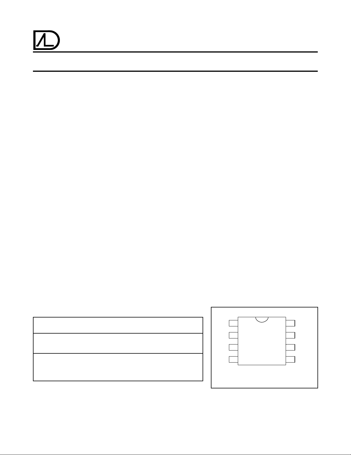
PIN CONFIGURATION
ORDERING INFORMATION
Operating Temperature Range
-55°C to +125°C0°C to +70°C0°C to +70°C
8-Pin 8-Pin 8-Pin
CERDIP Small Outline Plastic Dip
Package Package (SOIC) Package
ALD1701A DA ALD1701A SA ALD1701A PA
ALD1701B DA ALD1701B SA ALD1701B PA
ALD1701 DA ALD1701 SA ALD1701 PA
ALD1701G DA ALD1701G SA ALD1701G PA
* Contact factory for industrial temperature range
© 1998 Advanced Linear Devices, Inc. 415 T asman Drive, Sunnyvale, California 94089 -1706 Tel: (408) 747-1155 Fax: (408) 747-1286 http://www .aldinc.com
1
N/C
-IN
+IN
-
V
* N/C Pin is internally connected. Do not connect externally.
2
2
3
4
TOP VIEW
DA, PA, SA PACKAGE
8
N/C
+
7
V
6
OUT
5
N/C
ABSOLUTE MAXIMUM RATINGS
Supply voltage, V
Differential input voltage range -0.3V to V
Power dissipation 600 mW
Operating temperature range PA, SA package 0°C to +70°C
Storage temperature range -65°C to +150°C
Lead temperature, 10 seconds +260°C
+
13.2V
+
+0.3V
DA package -55°C to +125°C
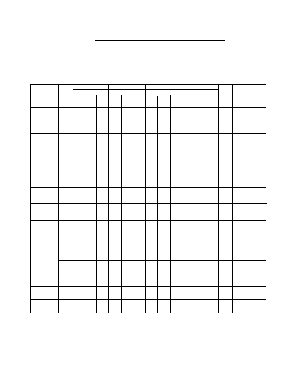
OPERATING ELECTRICAL CHARACTERISTICS
T
= 25°C V
A
Parameter Symbol Min Typ Max Min Typ Max Min Typ Max Min Typ Max Unit Conditions
Supply V
Voltage V
Input Offset V
Voltage 1.7 2.8 5.3 11.0 mV 0°C ≤ T
Input Offset I
Current 240 240 240 450 pA 0°C ≤ T
Input Bias I
Current 300 300 300 600 pA 0°C ≤ T
Input Voltage V
Range -2.8 2.8 -2.8 2.8 -2.8 2.8 -2.8 2.8 V V
Input R
Resistance
= ±2.5V unless otherwise specified
S
1701A 1701B 1701 1701G Test
±1.0 ±6.0 ±1.0 ±6.0 ±1.0 ±6.0 ±1.0 ±6.0 Dual Supply
S
+
2.0 12.0 2.0 12.0 2.0 12.0 2.0 12.0 V Single Supply
OS
OS
B
-0.3 5.3 -0.3 5.3 -0.3 5.3 -0.3 5.3 V V
IR
IN
10
0.9 2.0 4.5 10.0 mV R
1.0 25 1.0 25 1.0 25 1.0 30 pA T
1.0 30 1.0 30 1.0 30 1.0 50 pA T
12
10
≤ 100KΩ
S
≤ +70°C
A
= 25°C
A
≤ +70°C
A
= 25°C
A
≤ +70°C
A
+
= +5V
= ±2.5V
S
12
10
12
10
12
Ω
Input Offset TCV
OS
7777µV/°CR
S
≤ 100KΩ
Voltage Drift
Power Supply PSRR 70 80 65 80 65 80 60 80 dB R
Rejection Ratio 70 80 65 80 65 80 60 80 dB 0°C ≤ T
Common Mode CMRR 70 83 65 83 65 83 60 83 dB R
Rejection Ratio 70 83 65 83 65 83 60 83 dB 0°C ≤ T
Large Signal A
40 100 32 100 32 100 20 80 V/ mV R
V
Voltage Gain 1000 1000 1000 1000 V/ mV R
20 20 20 10 V/ mV R
Output VO low 0.001 0.01 0.001 0.01 0.001 0.01 0.001 0.01 V
≤ 100KΩ
S
≤ +70°C
A
≤ 100KΩ
S
≤ +70°C
A
= 100KΩ
L
≥ 1MΩ
L
= 100KΩ
L
≤ +70°C
0°C ≤ T
A
RL =1MΩ V+ = +5V
Voltage VO high 4.99 4.999 4.99 4.999 4.99 4.999 4.99 4.999 V 0°C ≤ TA ≤ +70°C
Range VO low -2.48 -2.40 -2.48 -2.40 -2.48 -2.40 -2.48 -2.40 V RL =100KΩ
VO high 2.40 2.48 2.40 2.48 2.40 2.48 2.40 2.48 V 0°C ≤ TA ≤ +70°C
Output Short I
SC
1 1 1 1 mA
Circuit Current
Supply Current I
S
120 250 120 250 120 250 120 300 µAV
IN
= 0V
No Load
Power P
D
1.25 1.25 1.25 1.50 mW V
= ±2.5V
S
Dissipation
ALD1701A/ALD1701B Advanced Linear Devices 2
ALD1701/ALD1701G
 Loading...