

Page 1

Product Specification
AHA4210 RSVP
Viterbi with
Reed-Solomon Decoder
Advanced Hardware
Architectures, Inc.
2365 NE Hopkins Court
Pullman, WA 99163-5601
509.334.1000
Fax: 509.334.9000
e-mail: sales@aha.com
http://www.aha.com
TM
Advanced Hardware
Architectures
The Data Coding Leader
PS4210-1099
Page 2

Advanced Hardware Architectures, Inc.
Notes to Customers of AHA4210
1) Patent(s) pending. One or more patent(s) have been applied for this product.
2
2) Purchase of I
Patent Rights to use these components in an I
system conforms to the I
C components of AHA conveys a license under the Philips I2C
2
C Standard Specification as defined by Philips.
2
C system, provided that the
PS4210-1099
Page 3

Advanced Hardware Architectures, Inc.
Table of Contents
1.0 Introduction . . . . . . . . . . . . . . . . . . . . . . . . . . . . . . . . . . . . . . . . . . . . . . . . . . . . . . . . . . . . . . . . . . . . . . . . . . . . .1
1.1 Applications. . . . . . . . . . . . . . . . . . . . . . . . . . . . . . . . . . . . . . . . . . . . . . . . . . . . . . . . . . . . . . . . . . . . . . . . . .1
1.2 Features . . . . . . . . . . . . . . . . . . . . . . . . . . . . . . . . . . . . . . . . . . . . . . . . . . . . . . . . . . . . . . . . . . . . . . . . . . . .1
1.3 Conventions and Notations. . . . . . . . . . . . . . . . . . . . . . . . . . . . . . . . . . . . . . . . . . . . . . . . . . . . . . . . . . . . . .1
1.4 Definition of Terms and Programmability . . . . . . . . . . . . . . . . . . . . . . . . . . . . . . . . . . . . . . . . . . . . . . . . . . .2
2.0 Functional Description . . . . . . . . . . . . . . . . . . . . . . . . . . . . . . . . . . . . . . . . . . . . . . . . . . . . . . . . . . . . . . . . . . . .3
2.1 Synchronization. . . . . . . . . . . . . . . . . . . . . . . . . . . . . . . . . . . . . . . . . . . . . . . . . . . . . . . . . . . . . . . . . . . . . . .3
2.1.1 Explanation of Clocking Schemes . . . . . . . . . . . . . . . . . . . . . . . . . . . . . . . . . . . . . . . . . . . . . . . . . .3
2.2 Viterbi Decoder . . . . . . . . . . . . . . . . . . . . . . . . . . . . . . . . . . . . . . . . . . . . . . . . . . . . . . . . . . . . . . . . . . . . . . .4
2.2.1 Depuncture. . . . . . . . . . . . . . . . . . . . . . . . . . . . . . . . . . . . . . . . . . . . . . . . . . . . . . . . . . . . . . . . . . . .4
2.3 Deinterleaver. . . . . . . . . . . . . . . . . . . . . . . . . . . . . . . . . . . . . . . . . . . . . . . . . . . . . . . . . . . . . . . . . . . . . . . . .4
2.4 RS Decoder. . . . . . . . . . . . . . . . . . . . . . . . . . . . . . . . . . . . . . . . . . . . . . . . . . . . . . . . . . . . . . . . . . . . . . . . . .5
2.5 Derandomize/Energy Dispersal. . . . . . . . . . . . . . . . . . . . . . . . . . . . . . . . . . . . . . . . . . . . . . . . . . . . . . . . . . .5
2.6 Modes of Operation. . . . . . . . . . . . . . . . . . . . . . . . . . . . . . . . . . . . . . . . . . . . . . . . . . . . . . . . . . . . . . . . . . . .5
2.7 Microprocessor Interface. . . . . . . . . . . . . . . . . . . . . . . . . . . . . . . . . . . . . . . . . . . . . . . . . . . . . . . . . . . . . . . .6
2.7.1 Parallel 80C188 Microprocessor Interface . . . . . . . . . . . . . . . . . . . . . . . . . . . . . . . . . . . . . . . . . . . .6
2.7.2 Serial I
2.8 Latency . . . . . . . . . . . . . . . . . . . . . . . . . . . . . . . . . . . . . . . . . . . . . . . . . . . . . . . . . . . . . . . . . . . . . . . . . . . . .8
2
C Protocol Interface. . . . . . . . . . . . . . . . . . . . . . . . . . . . . . . . . . . . . . . . . . . . . . . . . . . . . . .6
3.0 Register Description . . . . . . . . . . . . . . . . . . . . . . . . . . . . . . . . . . . . . . . . . . . . . . . . . . . . . . . . . . . . . . . . . . . . . .9
3.1 Register Summary. . . . . . . . . . . . . . . . . . . . . . . . . . . . . . . . . . . . . . . . . . . . . . . . . . . . . . . . . . . . . . . . . . . . .9
3.2 ERRSTAT: Error Count Status . . . . . . . . . . . . . . . . . . . . . . . . . . . . . . . . . . . . . . . . . . . . . . . . . . . . . . . . . . .9
3.3 ERRSIZE: Error Block Count. . . . . . . . . . . . . . . . . . . . . . . . . . . . . . . . . . . . . . . . . . . . . . . . . . . . . . . . . . . .10
3.4 VRSSIZE: Total Block Count for VRSTH . . . . . . . . . . . . . . . . . . . . . . . . . . . . . . . . . . . . . . . . . . . . . . . . . .10
3.5 VSYNCP: Sync Decoder Pattern. . . . . . . . . . . . . . . . . . . . . . . . . . . . . . . . . . . . . . . . . . . . . . . . . . . . . . . . .10
3.6 VRSTH: RS Uncorrectable Blocks Threshold. . . . . . . . . . . . . . . . . . . . . . . . . . . . . . . . . . . . . . . . . . . . . . .10
3.7 VERTH: Sync Control . . . . . . . . . . . . . . . . . . . . . . . . . . . . . . . . . . . . . . . . . . . . . . . . . . . . . . . . . . . . . . . . .1 0
3.8 VCON: Viterbi Control. . . . . . . . . . . . . . . . . . . . . . . . . . . . . . . . . . . . . . . . . . . . . . . . . . . . . . . . . . . . . . . . .11
3.9 MSGBYTES2: Message Bytes K. . . . . . . . . . . . . . . . . . . . . . . . . . . . . . . . . . . . . . . . . . . . . . . . . . . . . . . . .11
3.10 RSEED0: Derandomizer Seed LSB . . . . . . . . . . . . . . . . . . . . . . . . . . . . . . . . . . . . . . . . . . . . . . . . . . . . . .11
3.11 RSEED1: Derandomizer Seed MSB. . . . . . . . . . . . . . . . . . . . . . . . . . . . . . . . . . . . . . . . . . . . . . . . . . . . . .11
3.12 IOCNTRL: Input/Output Control . . . . . . . . . . . . . . . . . . . . . . . . . . . . . . . . . . . . . . . . . . . . . . . . . . . . . . . . .12
3.13 NJL: Block Length Times Interleave Depth LSB. . . . . . . . . . . . . . . . . . . . . . . . . . . . . . . . . . . . . . . . . . . . .12
3.14 NJM: Block Length Times Interleave Depth MSB. . . . . . . . . . . . . . . . . . . . . . . . . . . . . . . . . . . . . . . . . . . .12
3.15 BLKLEN2: RS Block Length N . . . . . . . . . . . . . . . . . . . . . . . . . . . . . . . . . . . . . . . . . . . . . . . . . . . . . . . . . .12
3.16 JDEPTH: Interleave Depth . . . . . . . . . . . . . . . . . . . . . . . . . . . . . . . . . . . . . . . . . . . . . . . . . . . . . . . . . . . . .13
3.17 RSCONTROL: Reed-Solomon Control. . . . . . . . . . . . . . . . . . . . . . . . . . . . . . . . . . . . . . . . . . . . . . . . . . . .13
4.0 Signal Descriptions and Specifications. . . . . . . . . . . . . . . . . . . . . . . . . . . . . . . . . . . . . . . . . . . . . . . . . . . . . .14
4.1 Input Signals . . . . . . . . . . . . . . . . . . . . . . . . . . . . . . . . . . . . . . . . . . . . . . . . . . . . . . . . . . . . . . . . . . . . . . . .14
4.2 Output Signals. . . . . . . . . . . . . . . . . . . . . . . . . . . . . . . . . . . . . . . . . . . . . . . . . . . . . . . . . . . . . . . . . . . . . . .15
4.3 Bidirectional Signals . . . . . . . . . . . . . . . . . . . . . . . . . . . . . . . . . . . . . . . . . . . . . . . . . . . . . . . . . . . . . . . . . .15
4.4 Input Specifications. . . . . . . . . . . . . . . . . . . . . . . . . . . . . . . . . . . . . . . . . . . . . . . . . . . . . . . . . . . . . . . . . . .16
4.5 Output Specifications. . . . . . . . . . . . . . . . . . . . . . . . . . . . . . . . . . . . . . . . . . . . . . . . . . . . . . . . . . . . . . . . . .16
4.6 Bidirectional Pin Specifications . . . . . . . . . . . . . . . . . . . . . . . . . . . . . . . . . . . . . . . . . . . . . . . . . . . . . . . . . .17
4.7 Power & Ground Pins . . . . . . . . . . . . . . . . . . . . . . . . . . . . . . . . . . . . . . . . . . . . . . . . . . . . . . . . . . . . . . . . .17
4.8 Pinout . . . . . . . . . . . . . . . . . . . . . . . . . . . . . . . . . . . . . . . . . . . . . . . . . . . . . . . . . . . . . . . . . . . . . . . . . . . . .17
5.0 Timing . . . . . . . . . . . . . . . . . . . . . . . . . . . . . . . . . . . . . . . . . . . . . . . . . . . . . . . . . . . . . . . . . . . . . . . . . . . . . . . . .18
6.0 DC Electrical Characteristics . . . . . . . . . . . . . . . . . . . . . . . . . . . . . . . . . . . . . . . . . . . . . . . . . . . . . . . . . . . . . .26
7.0 Packaging. . . . . . . . . . . . . . . . . . . . . . . . . . . . . . . . . . . . . . . . . . . . . . . . . . . . . . . . . . . . . . . . . . . . . . . . . . . . . .28
PS4210-1099 i
Page 4

Advanced Hardware Architectures, Inc.
8.0 Ordering Information. . . . . . . . . . . . . . . . . . . . . . . . . . . . . . . . . . . . . . . . . . . . . . . . . . . . . . . . . . . . . . . . . . . . .29
8.1 Available Parts. . . . . . . . . . . . . . . . . . . . . . . . . . . . . . . . . . . . . . . . . . . . . . . . . . . . . . . . . . . . . . . . . . . . . . .29
8.2 Part Numbering. . . . . . . . . . . . . . . . . . . . . . . . . . . . . . . . . . . . . . . . . . . . . . . . . . . . . . . . . . . . . . . . . . . . . .29
9.0 AHA Related Technical Publications. . . . . . . . . . . . . . . . . . . . . . . . . . . . . . . . . . . . . . . . . . . . . . . . . . . . . . . .29
10.0 Other Technical Publications . . . . . . . . . . . . . . . . . . . . . . . . . . . . . . . . . . . . . . . . . . . . . . . . . . . . . . . . . . . . . .30
ii PS4210-1099
Page 5

Advanced Hardware Architectures, Inc.
Figures
Figure 1: AHA4210 Block Diagram . . . . . . . . . . . . . . . . . . . . . . . . . . . . . . . . . . . . . . . . . . . . . . . . . . . . . . . . . . . . .3
2
Figure 2: I
Figure 3: I
Figure 4: Bit Transfer . . . . . . . . . . . . . . . . . . . . . . . . . . . . . . . . . . . . . . . . . . . . . . . . . . . . . . . . . . . . . . . . . . . . . . . .8
Figure 5: Start and Stop Conditions. . . . . . . . . . . . . . . . . . . . . . . . . . . . . . . . . . . . . . . . . . . . . . . . . . . . . . . . . . . . .8
Figure 6: Clock Timing - SCLK and VCLK. . . . . . . . . . . . . . . . . . . . . . . . . . . . . . . . . . . . . . . . . . . . . . . . . . . . . . .18
Figure 7: Reset Timing. . . . . . . . . . . . . . . . . . . . . . . . . . . . . . . . . . . . . . . . . . . . . . . . . . . . . . . . . . . . . . . . . . . . . .18
Figure 8: DATAFLUSH Timing - Byte Input Mode . . . . . . . . . . . . . . . . . . . . . . . . . . . . . . . . . . . . . . . . . . . . . . . . .19
Figure 9: Microprocessor Write Timing . . . . . . . . . . . . . . . . . . . . . . . . . . . . . . . . . . . . . . . . . . . . . . . . . . . . . . . . .19
Figure 10: Microprocessor Read Timing . . . . . . . . . . . . . . . . . . . . . . . . . . . . . . . . . . . . . . . . . . . . . . . . . . . . . . . . .20
Figure 11: I
Figure 12: Input - Serial Mode: IOCNTRL[2:1] = 0x Mode. . . . . . . . . . . . . . . . . . . . . . . . . . . . . . . . . . . . . . . . . . . .22
Figure 13: Input - Byte Mode: IOCNTRL[2:1] = 10 Mode. . . . . . . . . . . . . . . . . . . . . . . . . . . . . . . . . . . . . . . . . . . . .22
Figure 14: Input - Byte Mode IOCNTRL[2:1] = 11 . . . . . . . . . . . . . . . . . . . . . . . . . . . . . . . . . . . . . . . . . . . . . . . . . .23
Figure 15: Output - BCLK Mode: IOCNTRL[4:3] = 10, [2:1] = 11. . . . . . . . . . . . . . . . . . . . . . . . . . . . . . . . . . . . . . .24
Figure 16: Output - Byte Mode: IOCNTRL[4:3] = 10, IOCNTRL[2:1] ≠11 . . . . . . . . . . . . . . . . . . . . . . . . . . . . . . . .24
Figure 17: IOCNTRL[4:3] = 00, Serial Output . . . . . . . . . . . . . . . . . . . . . . . . . . . . . . . . . . . . . . . . . . . . . . . . . . . . .2 5
Figure 18: IOCNTRL[4:3] = 01, Serial Output . . . . . . . . . . . . . . . . . . . . . . . . . . . . . . . . . . . . . . . . . . . . . . . . . . . . .2 5
Figure 19: IOCNTRL[4:3] = 10, Byte Output . . . . . . . . . . . . . . . . . . . . . . . . . . . . . . . . . . . . . . . . . . . . . . . . . . . . . .25
Figure 20: IOCNTRL[4:3] = 11, Byte Output . . . . . . . . . . . . . . . . . . . . . . . . . . . . . . . . . . . . . . . . . . . . . . . . . . . . . .25
Figure 21: Power vs. VCLK Rate, Estimated for Modes 1 and 3 . . . . . . . . . . . . . . . . . . . . . . . . . . . . . . . . . . . . . . .27
Figure 22: Max Ambient Temperature (Ta) vs. VCLK Rate, Estimated for Modes 1 and 3. . . . . . . . . . . . . . . . . . .27
C Internal Register Increment Example, Writing the Registers . . . . . . . . . . . . . . . . . . . . . . . . . . . . . . .7
2
C Reading Internal Registers . . . . . . . . . . . . . . . . . . . . . . . . . . . . . . . . . . . . . . . . . . . . . . . . . . . . . . . . .7
2
C Interface Timing . . . . . . . . . . . . . . . . . . . . . . . . . . . . . . . . . . . . . . . . . . . . . . . . . . . . . . . . . . . . . . . .21
PS4210-1099 iii
Page 6

Advanced Hardware Architectures, Inc.
Tables
Table 1: Various Modes Supported by the AHA4210 Device. . . . . . . . . . . . . . . . . . . . . . . . . . . . . . . . . . . . . . . . .5
Table 2: Register Settings for Functional Block Bypass. . . . . . . . . . . . . . . . . . . . . . . . . . . . . . . . . . . . . . . . . . . . .5
Table 3: Maximum Latency in VCLK Cycles. . . . . . . . . . . . . . . . . . . . . . . . . . . . . . . . . . . . . . . . . . . . . . . . . . . . . .8
iv PS4210-1099
Page 7

Advanced Hardware Architectures, Inc.
1.0 INTRODUCTION
The AHA4210, referred to as the RSVP, is a
single-chip Forward Error Correction LSI device
combining a Viterbi decoder, a Reed-Solomon
decoder, a descrambler (energy dispersal) and a
deinterleav er. The de vice c onforms to the MPEG-II
transport layer protocol specified by ISO/IEC
standard and FEC requirements of Digital Video
Broadcasting (DVB) DT/8622/DVB and DT/8610/
III-B specif ication. These documen ts are referr ed to
as the DVB specification.
The Viterbi decoder supports selectable code
rates of 1/2, 2/3, 3/4, 5/6, 6/7 or 7/8 using industry
standard puncturing algorithms. Viterbi decoded
data rate is up to 62 Mbits/second at all code rates.
The chip also performs byte alignment and block/
packet synchron ization detecti ng sync bytes use d in
transmission. The descrambling function is
selectable with a programmable seed or performed
externally. Each fun ctional block may be bypassed
giving more flexibility to a system designer.
Block size programmability, several code rate
choices and programmable RS error correction
capability allows flexibility to a digital
communications system designer incorporating
Forward Error Correction into a receiver. Intel
80C188 multiplexed parallel or serial I
interface allows the system microprocessor to
program internal registers and monitor channel
performance.
This document contains ke y featu re s,
correction terms, functional description, signal
functions, Related Technical Publications, DC and
AC characteristics, pinout, package dimension and
ordering information.
1.1 APPLICATIONS
• Satellite communications/VSAT
• DBS
• Military Communications
1.2 FEATURES
GENERAL:
• Conforms to the ISO/IEC-CD 13818-1 MPEG-II
transport layer protocol and Digital Video
Broadcasting (DVB)FEC specification
• Viterbi decoded data rates up to 62 Mbits/sec at
any code rate
• Programmable block size from 34 to 255 bytes
• Multiplexed parallel Intel 80C188 or serial I
protocol microprocessor interface
• Byte or serial data output
• On-Chip err or rate monitor
2
C protocol
2
C
• Programmable bypass modes for each of the
major blocks
• Configured to DVB mode of operation on
power-up
• 68 pin PLCC
VITERBI DECODER:
• Selectable decoder rates 1/2, 2/3, 3/4, 5/6, 6/7
and 7/8 or automatic acquire mode
• 3-Bit soft-decision decoder inputs
• Constraint length k=7
SYNCHRONIZATION CONTROL:
• Automatic synchronization capability for QPSK
based demodulator
• Up to one sync byte per block
• Responds to inverted sync byte
REED-SOLOMON:
• t=1 through 8 in increments of 0.5
• Correction capability of up to 8 bytes
• Internal FIFOs
DEINTERLEAVER:
• Programmable convolutional deinterleaving
(Ramsey II, Ramsey II modified or Forney) to
depth I=16
• No externa l RAM required
ENERGY DISPERSAL:
• Selectable on-chip DVB specification Energy
Dispersal
• Optional bypass mode
• Programmable seed
1.3 CONVENTIONS AND NOTATIONS
- Cert ain signals are logically true at a voltage
defined as “low” in the data sheet. All such
signals have an “N” appended to the end of the
signal name. For example, RSTN and RDYON.
- “Signal assertion” means the signal is logically true.
- Hex values are defined with a prefix of “0x”,
such as “0x10”.
- A range of signal names is denoted by a set of
colons between the numbe rs . Most signi f ican t b it
is always shown first, followed by least
significant bit. For example, ERRSTAT[6:0]
represents number of bytes corrected by the
Reed-Solomon decoder.
- A product of two variables is expressed with an
“x”, for example, BLKLEN2 x JDEPTH
represents Block Length mu ltip lied b y Int erle a ve
Depth.
- Megabytes per second is referred to as MBytes/
sec or MB/sec. Megabit s per second i s referred as
Mbits/sec or Mb/sec.
- Frequency of a clock signal is referred to as
F(name). For example, F(VCLK) specifies
frequency of VCLK.
PS4210-1099 Page 1 of 30
Page 8
Advanced Hardware Architectures, Inc.
1.4 DEFINITION OF TERMS AND PROGRAMMABILITY
VITERBI
TERM
k Constraint Length
NAME
(other references)
Number of input bits over which convolutional
code is computed.
Length of path through the trellis over which the
Traceback Depth
Viterbi decoder computes the likelihood of a
decoded bit value.
Puncturing
Puncture Pattern
Convolutional Code
Rate (Puncture Rate)
Process of deriving a higher rate code from a basic
rate code.
Mapping between 1/2 rate encoded bits and new
higher rate encoded bits.
Ratio of input to output bits for convolutional
code.
DEINTERLEAVER
TERM
Ramsey or Forney Convolutional interleave techniques. N/A
J Interleave Depth Minimum separation in th e interleaved stream. 1 through 16
NAME
(other references)
DEFINITION RANGE
7
minimum=115
N/A
N/A
1/2, 2/3, 3/4, 5/6, 6/
7, 7/8
DEFINITION RANGE
TERM
K
R
N
Message Length (user
data or message bytes)
Check symbols
(parity or redundancy)
Codeword Length
(block length)
NAME
(other references)
t Error Corrections
e Number of Errors
RS Code Rate Ratio of message to block length, . 0.67 through 0.99
TERM
NAME
(other references)
Bypass
Block
Packet MPEG-II transport layer packet size.
REED-SOLOMON
DEFINITION RANGE
Number of user data symbols in one message
block. Size of a symbol in AHA4210 is 8-bits.
Message length is .
KNR–=
Symbols appended to the user data to detect and
correct errors. The number of check symbols
required in a sys te m is . Every 2 ch ec k bytes
R 2e≥
correct 1 error byte.
Sum of message and check symbols. .
NKR+=
Maximum number of error corrections performed
by the device. The value is t=Integer .
NK–
-------------2
An error is defined as an erroneous byte whose
correct value and position within the message
block are both unknown.
K
--- -
GENERAL
DEFINITION RANGE
Processing data either through or around a
functional block.
An entity of both message and Reed-Solomon check
bytes. The number of message bytes is equal to the
length of the MPEG-II packet for a DVB system.
32 thru 253 bytes
(32, 33, 34 . . . 253)
2 thru 16 bytes in
increments of 1
(2, 3, 4 . . . 16)
34 thru 255 bytes
(34, 35, 36 . . . 255)
1 thru 8 bytes in
increments of 0.5
(1, 1.5, 2, 2.5 . . . 8)
minimum 0
N/A
(34, 35, . . . 255)
bytes
188 including one
sync mark byte
Page 2 of 30 PS4210-1099
Page 9
Advanced Hardware Architectures, Inc.
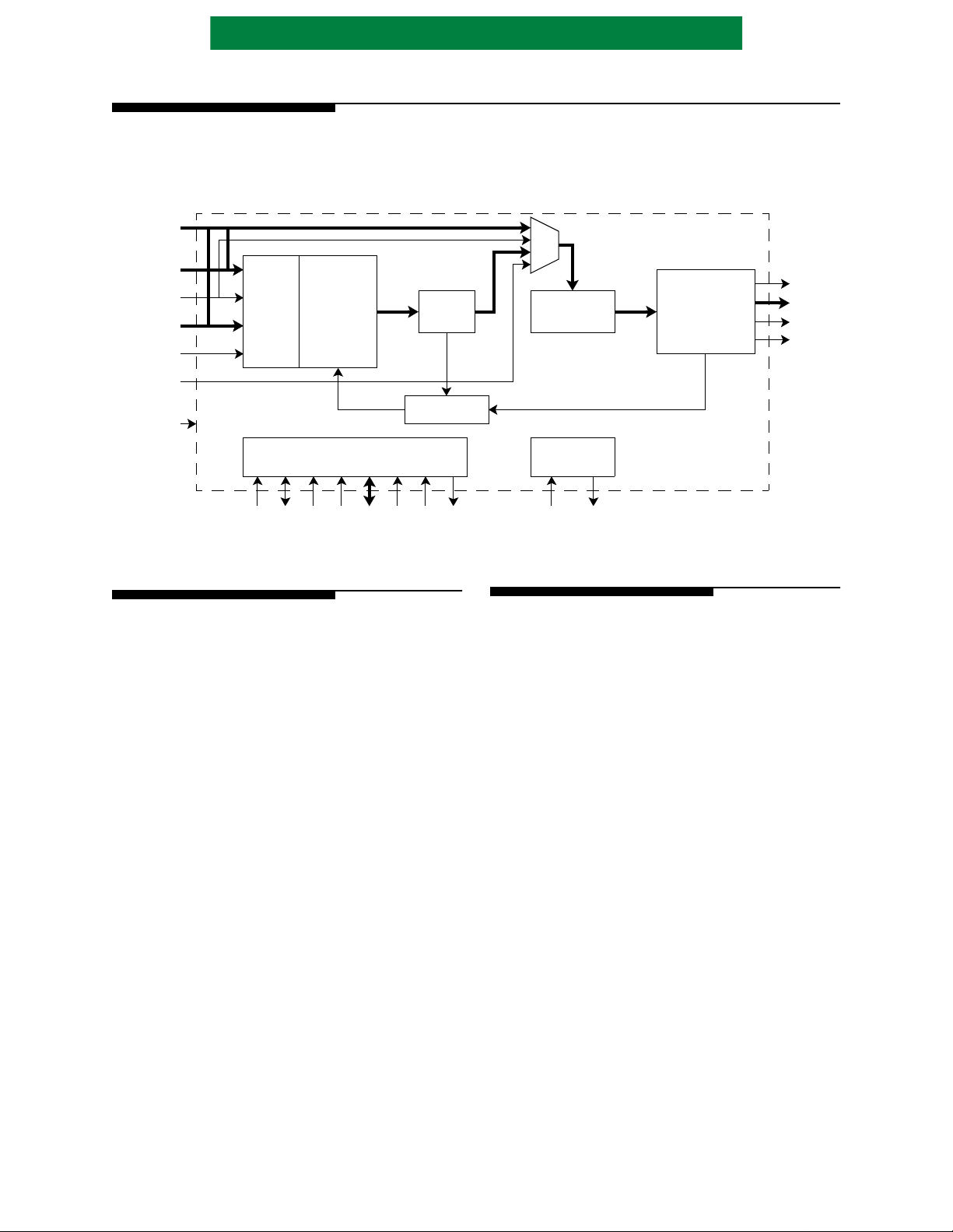
2.0 FUNCTIONAL DESCRIPTION
This section presents an architectural overview of the chip and its many functions, features and
operating modes. Block diagram of the chip shows the Viterbi and Reed-Solomon decoder modules.
Figure 1: AHA4210 Block Diagram
BYTE[1:0]
MUX
I[2:0]
IQSTRB
Q[2:0]
SCLK
DATAFLUSH
INPUT
INTERFACE
DEPUNCTURING
LOGIC
VITERBI
DECODER
DEINTERLEAVER
&
RAM
REED-SOLOMON
DECODER
&
ENGERY DISPERSAL
(DESCRAMBLER)
BLKNEW
DO[7:0]
RDYON
BLKERR
MD[7:0]
SYNC CONTRO L
MAL
MCSN
RSTN
MICROPROCESSOR INTERFACE
DECODER CONTROL
SCL
SDA
MRDN
MWRN
2.1 SYNCHRONIZATION
This module synchronizes data received from
Viterbi to byte and packet boundaries. The
synchronization alg ori thm is summarized below.
Bit-to-byte mapping is performed while
looking for sync marks specified in register
VSYNCP . Ev ery bit posit ion is examine d for a sync
mark byte. If no sync mark is d etected af ter looking
for a minimum of two block lengths, then the phase
is incremented and the process is repeated. Carrier
and depuncture phases are cycled through
searching for sync marks. This process terminates
when sync is achieved.
After a sync mark is detected, additional sync
marks as specified in SYNCON[2:0] are searched.
Detection of additional sync completes the block
sync process and da ta is out put on th e ne xt in v er ted
sync (or regular sync if VCON[7] = 0). Once the
output data flow starts, cons ecu tive sync marks are
required if enabled by the VCON[6] to remain in
sync. In this case if SYNCOFF[2:0] consecutive
sync marks are missed, then the block goes out of
the sync condition.
The block may also go out of sync if the ReedSolomon uncorrectable blocks threshold is
exceeded over a programmable number of blocks.
This feature is enabled by VCON [5]. Total Block
Count and Threshold are programmed by
VRSSIZE and VRSTH registers.
DECODER
CLOCK CONTR OL
VCLK
READY
BCLK
2.1.1 EXPLANATION OF CLOCKING SCHEMES
The Viterbi block has two clock inputs: SCLK
and VCLK. VCLK runs the actual Viterbi decoder
block while SCLK simply d riv es the in put stage for
V iterbi. The data inp uts I[2:0], Q[2:0] and IQSTRB
are synchronous to SCLK.
There are two approaches to using this
interface. Approa ch one involves tying IQSTRB to
VDD (active) and assuring that:
VCLK
Frequency SCLK()Frequency
≤
Where CR is defined as the code ra te. Note that
this is a strict requi re me nt and the chi p will enter a
state requiring a hard reset if this is not met.
One advantage to this approach is that in some
designs SCLK is already available and I and Q are
already synchronous to this signal.
The other method is to tie SCLK and VCLK
together and throttle the data with IQSTRB. For
X
any given code rate , where Y is even, IQSTRB
would be held high (clocking in I[2:0] and Q[2:0]
---
Y
on that cycle) for no more than out of every X
clocks. If Y is odd then IQSTRB woul d be held high
for no more than Y out of every 2X clocks and no
Y 1+
more than in every X clock cycles.
In the final approach it is not necessary to
-----------2
supply a separate clock (SCLK), however, the
customer must supply the circuitry to drive
IQSTRB appropriately.
---------------- -
2 CR×
Y
-- 2
PS4210-1099 Page 3 of 30
Page 10
Advanced Hardware Architectures, Inc.
F SCLK()
F VCLK()
2 CR×
------------------------
≤
The Viterbi decoder can be set up to cycle
through all convolutional code rates. In this case,
use convolutional code rate ≥ 7/8 in the equation:
2.2 VITERBI DECODER
The Viterbi decoder takes the data from an I
and a Q channel and decode s these using a 3 bit sof t
decision. The V i terbi d ecoder is bas ed on a 1/2 rate
code, but also sup ports punctu red cod es with ra tes:
2/3, 3/4, 5/6, 6/7 and 7/8.
The generator polynomials are:
g1 171(octal) and g2 133(octal)==
The minimum trace back depth is 115.
The output of the Viterbi decoder is converted
to 8 bit bytes, sync bytes are det ected and after
which the data is run through the deinterleaver to
restore the ECC blocks.
The V iterbi deco der can be bypass ed by bit 2 of
the IOCNTRL and disabled by bit 4 of the VCON
register.
The latency of th e Viterbi block is measured in
two ways. First, there is a latency associated with
“synching” to the incoming signal. Assuming that
there is no valid sync byte patterns in the data the
worst case sync time is given by:
8 block length 384+×()4 # of puncture phases()512+××
This assumes that SCLK runs fast enough to
keep the data pi peline full. Once the V iterbi block is
synched up, the maximum latency from input to
output is 258 VCLK cycles.
2.2.1 DEPUNCTURE
The Viterbi module can be programmed to
depuncture according to a specified code rate or
automatically find the code rate used in the channel.
Follo wing i s a lis t of punc ture p att erns a nd number
of phases that are cycled through in an attempt to
align the puncture phase.
RATE PATTERN: X:Y # OF PHASES
1/2
2/3
3/4
5/6
6/7
7/8
X
Y
X
Y
X
Y
X
Y
X
Y
X
Y
1000101
1111010
10
11
101
110
10101
11010
100101
111010
1
1
1
3
2
3
7
4
During the encoding process, X and Y are
mapped into I and Q b y taking the nond eleted terms
in order of X1, Y1, X2, Y2, etc. Deleted terms are
simply skipped. The decodi ng process is si mply the
reverse of this procedure. Erasures are inserted on
the pattern locations with zeroes. For example, the
rate 5/6 I and Q have values:
I = X1, Y2, Y4, X1, Y2, Y4, . . .
Q = Y1, X3, X5, Y1, X3, X5, . . .
The chip is capable of supporting a limited
number of depuncture codes not included in this
specification. The procedure for supporting these
codes are beyond the scope of this specification.
Please contact AHA Applications Engineering for
these codes.
The Viterbi core can be configured to self
synchronize to the appropriate depuncture pattern
phase and correct for phase ambiguity. If
VRSSIZE[6] is set, Viterbi sync does not cycle
pi
---- 2
through carrier phases. If the code rate is not
known, the core can also be con figured to cycle
through 1/2, 2/3, 3/4, 5/6, 6/7 and 7/8 code rates
looking for a valid pattern.
2.3 DEINTERLEAVER
The deinterleaver supports a variety of
programmed options:
TECHNIQUE TYPE
WITH
VITERBI
Ramsey II No Yes
Forney/Ramsey III Yes Yes
Modified Ramsey II Yes Yes
A Ramsey type II interlea ver is spe cified in J .L.
Ramsey, “Realization of Optimal Interleavers,”
IEEE Transaction on Information Theory, May
1970, pp. 338-345. A F orne y/Ramse y ty pe III int erleaver is specified in DVB DT/8622/DVB
specifica tion. The interleave dept h is programmable
up to 16 packets and the bl ock size is programmable
up to 255 bytes. However, the product of the interleave depth and block length cannot be larger than
2688 bytes. In a ddi ti on t o t hi s, t he following co ndi tions must be satisfied for various applications.
APP INTERLEAVE CONSTRAINT
Forney/
DVB
Ramsey III
Ramsey II
Ramsey II
modified
Maximum processing latency =
8 NJM[3:0] & NJL[7:0]()× VCLKS
Note that the “&” is a concatenation symbol.
BLKLEN2/JDEPTH[3:0]
must be an integer
BLKLEN a nd JD EPTH [3:0 ]
must be relati vely prime
Same as Ramsey II
WITHOUT
VITERBI
Page 4 of 30 PS4210-1099
Page 11
Advanced Hardware Architectures, Inc.
px() x8x4x3x21++++=
α1primitive element=
2.4 RS DECODER
The RS block performs the ou ter decoding. The
Reed-Solomon decoder conforms to the DVB
specificati on. Th e RS bl ock can be programmed to
decode t=1, 1.5, 2, . . . 7.5, 8.
2t 1–
gx() x α0+()x α1+(). . . x α
The block length of the code is programmable
up to 255 bytes. Block length is 204 with 16 check
bytes and a correction power of 8 bytes per block
for the DVB specification. Maximum latency
through the RS Decoder Block is:
N 1–()81202RN2.67×+++×
()
+()=
2.5 DERANDOMIZE/ENERGY
DISPERSAL
The derandomizer is specified in the DVB
specification. It is built as a 15 stage pseudorandom binary sequence generator with
initialization sequence specified by RSEED0 and
RSEED1 registers. The randomization occurs over
8 blocks of MGSBYTES2 (188 bytes for DVB
specification). Randomization does not occur over
Reed-Solomon parity bytes nor sync bytes.
However, the pseudo-random binary sequence
generator continue s to run during non-in verted sync
bytes. Maximum latency = 10 VCLKs.
2.6 MODES OF OPERATION
The FEC decoder has been designed with a
modular approach so that each of the four major
functions: Viterbi deco ding, deinterle aving, RS
decoding and derandomization can be individually
enabled or disabled. Five operating modes are
supported by the device. These are:
1) Normal mode. All functions enabled. Inputs
clocked with SCLK.
2) Byte Input mode. All functions except Viterbi
enabled. Inputs clocked with VCLK. Tie
SCLK to VCLK. Use Byte [1:0], I[2:0] and
Q[2:0] as byte wide data path. Bytes must
arrive on packet boundaries.
3) Viterbi decode mode. Inputs clocked with
SCLK.
4) Reed-Solomon decode mode. Same input
constraints as byte input mode.
5) Deinterleave mode. Same input constraints as
byte input mode.
These modes may be operated with or without
the derandomizer enabled.
Table 1: Various Modes Supported by the AHA4210 Device
FUNCTIONAL BLOCK
MODE
VITERBI DEINTERLEAVER RS DECODER DERANDOMIZER
1) Normal Enabled Enabled Enabled Either
2) Byte Input Disabled Enabled Enabled Either
3) Viterbi Decode Enabled Disabled Disabled Either
4) RS Decode Disabled Disabled Enabled Either
5) Deinterleaver Disabled Enabled Disabled Either
Ta ble 2: Register Settings for Functional Block Bypass
FUNCTIONAL BLOCK ENABLED DISABLED
Viterbi
Deinterleaver JDEPTH[4]=1 JDEPTH[4]=0
Reed-Solomon RSCONTROL=0C RSCONTROL=1C
Derandomizer IOCNTRL[7]=1; VCON[7]=1 IOCNTRL[7]=0; VCON[7]=0
VCON[4]=1
IOCNTRL[2]=0
VCON[4]=0
IOCNTRL[2]=1
PS4210-1099 Page 5 of 30
Page 12

Advanced Hardware Architectures, Inc.
2.7 MICROPROCESSOR INTERFACE
The device is capable of interfacing to a
multiplexed eight bit bus or the I
The system microproc essor is referr ed to as the host
and behav es as a “mast er” a nd the AHA device is a
“slave.”
2.7.1 PARALLEL 80C188 MICROPROCESSOR
INTERFACE
The parallel inte rface suppo rts an Intel 8 0C188
microprocessor wit h a multiplexed ad dress and data
bus. For a register read operation the chip select
(MCSN) is asserted. The device asserts the READ Y
signal low. This is followed by the host outputting
the register add ress on the MD[ 7:0] bus along with
the address latch enable (MAL). The host then
asserts the read strobe (MRDN). The device
responds by outputting t he data o n the MD[7:0] b us
and tristating the READY signal. Valid data is
available when READY is tristated by the device.
Bus cycle is terminated by the host deasserting the
MRDN signal.
A register write operation is si milar to the
register read except the host asserts the MWRN
strobe along with the data. The device then loads
the data into the appropriate register and tristates
the READ Y signal. The bus cyc le termi nates when
the MWRN strobe gets deasserted.
When using th e parallel interface tie the SCL
and the SDA signals high. MCSN must not glitch
2.7.2 SERIAL I2C PROTOCOL INTERFACE
2
C serial interfa ce.
Publications section. This device works in either
high speed mode or standard low speed mode.
In high speed mode, the f irst tw o bytes be tween
a host and a slave device determine the device
selected. These two bytes are the first two bytes
following the Start condition as shown in Figure 5.
The bytes contain: 1, 1, 1, 1, 0, AD4, AD3, R/
W, and AD2, AD1, AD0, A4, A3, A2, A1, A0.
AD[4:0] = Slave ID address
A[4:0] = Register address
R/W = Direction of data transfer where:
1 = Read; 0 = Write
When programming the registers in I
the device performs auto increment of internal
addresses. All 16 addresses may be accessed by
writing 21 values to Address 0x00 as shown in
Figure 2. Alternatively a register may be randomly
accessed by specifying its address, such as 0x04.
Figure 2 is an example of writing to one or
more registers. Fig ure 3 is an example of reading a
register.
The serial I
2
the I
C Bus Specification. For electrical
2
C interface protocol conforms to
performance of this interface, please refer to th e
Timing section.
Notes:
1) This document contains a very brief description of
2) I
.
3) See Note 2 on back of cover page.
2
C Bus functions. For a detailed description,
the I
please refer to Specification documents available
from Philips.
2
C Bus pr otocol supported by AHA4210 requires a
10-bit addressing.
2
C mode,
The I2C interface is a serial microprocessor
interface using two signals named SCL and SDA.
Any drivers connected to these signals must be
open drain or open collector to facilitate the wiredAND operation of this b us . There is o ne SCL pul se
per data bit and the SDA line must be stable during
the high period of the SCL pulse, changing only
when SCL is low for data transfers.
In a target desi gn usi ng th e I
2
C serial interf ace,
the following connections need to be made.
Connect MRDN and MWRN to Ground. Tie
MCSN high and connect MAL to Ground. The
lower five bits of the MD[7:0] bus need to be
hardwired to the correct Slave ID address. For
example, if a Slave ID address of 5 is needed,
connect bits 0 and 2 to VDD, and bits 1, 3 and 4 to
Ground.
The following paragraphs describe briefly the
serial communication over this bus. For more
detailed information please refer to the I
2
C Bus
Specification listed in the Related Technical
Page 6 of 30 PS4210-1099
Page 13

Advanced Hardware Architectures, Inc.
Figure 2: I2C Internal Register Increment Example, Writing the Register s
ST 1 1 1 1 0 AD4 AD3 R/W ACK
Acknowledge
Direction
MSB’s of ID
Address (Hard Wired)
Special Co de for
10-bit Addressing
Start Condition
AD2 AD1 AD0 A4 A3 A2 A1 A0 ACK
Acknowledge
5 bits of Internal
Register Addressing
(Start Address)
3 LSB’s of ID Address
(Hard Wired)
BYTE 0 ACK
BYTE 1 ACK
BYTE 2 ACK STP
Figure 3: I2C Reading Internal Registers
ST 1 1 1 1 0 AD4 AD3 R/W ACK
AD2 AD1 AD0 A4 A3 A2 A1 A0 ACK
Sr 1 1 1 1 0 AD4 AD3 R/W ACK
Data
Stop Condition
’ is generated by the mas ter
An ‘ACK
device on termination of read operation.
Write, Set to 0
Internal Regis t er
Address
Read, Set to 1
Repeated Start
Register Read Data ACK
STP
PS4210-1099 Page 7 of 30
Page 14

Advanced Hardware Architectures, Inc.
Figure 4: Bit Transfer
SDA
SCL
Figure 5: Start and Stop Conditions
SDA
MSB
Acknowledge
SCL
Start Condition Stop Condition
12 89
2.8 LATENCY
Maximum latency measured in VCLK cycles
through the various blocks is summarized in
Table 3.
Table 3: Maximum Latency in VCLK Cycles
FUNCTIONAL
BLOCK
Vi terb i 258 (after sync has be en acqui red)
Deinterleaver 8 x (NJM[3:0] & NJL[7:0])
RS Decoder (N-1)x8+120+2R+Nx2.67
Derandomizer 10
LATENCY
Page 8 of 30 PS4210-1099
Page 15

Advanced Hardware Architectures, Inc.
3.0 REGISTER DESCRIPTION
This section contains a summary and a desc ription of re gisters. Unless otherwise spec ified , all regi sters
are Read/Write. The following registers can be changed during operation: ERRSIZE, VRSSIZE[5:0],
VSYNCP, VRSTH, VERTH, VCON[3:0], RSEED0 and RSEED1. The other registers must be
programmed before the first data is input to the AHA4210 after a reset.
3.1 REGISTER SUMMARY
FUNCTIONAL
BLOCK
Error Monitor
Viterbi and
Synchronizer
Derandomizer
Deinterleaver
Reed-Solomon 0x0F
ADDRESS MNEMONIC REGISTER NA ME
0x00 ERRSTAT Error Count 0x00
0x01 ERRSIZE Total Block Count for ERRSTAT 0x20
0x02 VRSSIZE Total Block Count for VRSTH 0x18
0x03 VSYNCP Sync Decoder Pattern 0x47
0x04 VRSTH Reed-Solomon Uncorrectable Blocks Threshold 0x08
0x05 VERTH Sync Control 0x27
0x06 VCON Viterbi Control 0xB3
0x07 MSGBYTES2 Message bytes, k 0xBC
0x08 RSEED0 Derandomizer seed, LSB 0xA9
0x09 RSEED1 Derandomizer seed, MSB 0x00
0x0A IOCNTRL Input/Output Control 0x90
0x0B NJL Block Length times Interleave Depth, LSB 0x90
0x0C NJM Block Length times Interleave Depth, MSB 0x09
0x0D BLKLEN2 Reed-Solomon Block Length, N 0xCC
0x0E JDEPTH Interleave Depth 0x1C
RES
RES
CHKBYTES
MSGBYTES
BLKLEN
RSCONTROL
Reserved
Reserved
Check bytes
Message bytes
Block Length
Reed-Solomon Control
RESET
VALUE
0xFF
0xFF
0x90
0xBC
0xCC
0x0C
Notes:
1) Reed-Solomon registers, address 0x0F, are Write only. All other registers are Read/Write.
2) All six registers of the Reed-Solomon block must be programmed consecutively. Write to address 0x0F accesses
these registers.
3) On Reset, the AHA4210 device is configured for DVB specification operation.
3.2 ERRSTAT: ERROR COUNT STATUS
Address: 0x00; Reset Value = 0x00
BIT DESCRIPTION
1 = One or more blocks within ERRSIZE is flagged uncorrectable. Bits [6:0] values do not
7
6:0
PS4210-1099 Page 9 of 30
represent total corrected locations.
0 = Errors have been corrected. Bits [6:0] represent to tal corrected locations.
Number of bytes cor re ct ed by RS in ERRSIZE blocks. The se bits should be ignored when bit [7]
is set to ‘1’ or when RS is bypassed. If the number of errors exceeds 126, then the value in this
register saturates at 127.
Page 16

Advanced Hardware Architectures, Inc.
3.3 ERRSIZE: ERROR BLOCK COUNT
Address: 0x01; Reset Value = 0x20
BIT DESCRIPTION
7:0 Total number of blocks over which ERRSTAT counts corrected bytes by Reed-Solomon.
3.4 VRSSIZE: TOTAL BLOCK COUNT FOR VRSTH
Address: 0x02; Reset Value = 0x18
BIT DESCRIPTION
7 Reserved. Set to ‘0’.
6 If set, then Viterbi sync does not cycle through carrier phases.
5:0
The number of total blocks over which the number of uncorrectable blocks is counted and
compared to the VRSTH value.
3.5 VSYNCP: SYNC DECODER PATTERN
Address: 0x03; Reset Value = 0x47
BIT DESCRIPTION
7:0 The value of the sync byte. The inverted sync value is derived from VSYNCP.
3.6 VRSTH: RS UNCORRECTABLE BLOCKS THRESHOLD
Address: 0x04; Reset Value = 0x08
BIT DESCRIPTION
7:4 Reserved. Set to ‘0’.
3:0 RSOFF is Reed-Solomon uncorrectable blocks threshold.
3.7 VERTH: SYNC CONTROL
Address: 0x05; Reset Value = 0x27
BIT DESCRIPTION
7 Reserved. Set to ‘0’.
SYNCON is the number of sync bytes that must be detected before the synchronization block
6:4
3
2:0
claims synchronizat ion has been achieved. Minimum value i s 2. Values of 0 a nd 1 are illegal and
result in unknown operation. See Inverted Sync Note.
Specify mapping number on the input signal.
0 = mapping #1
0 = strongest zero, 3 = weakest zero
4 = weakest one, 7 = strongest one
1 = mapping #2
3 = strongest zero, 0 = weakest zero
4 = weakest one, 7 = strongest one
SYNCOFF is the number of sync bytes that must be missed before the synchronization block
claims synchronization has been lost. 0 is illegal. See Inverted Sync Note.
Inverted Sync Note:
When the SYNCON value is set to ‘010’ and VCON[7]= 1, the AHA4210 can sync onto an inverted data st ream, such as
can occur if the demod is 180 degrees out of phase. When SYNCOFF value is set to ‘111’ and VCON[7:5] is set to ‘110’
or ‘100’, the AHA4210 does not go out of sync when an inverted data stre am occurs. In either case, enabling the ReedSolomon error r ate control over resynchronization VCON[5] causes the AHA4210 to r e cover from these conditions.
Page 10 of 30 PS4210-1099
Page 17

Advanced Hardware Architectures, Inc.
3.8 VCON: VITERBI CONTROL
Address: 0x06; Reset Value = 0xB3
BIT DESCRIPTION
7 1 = enable, 0 = disable inverted sync detection.
6
5
4
3 1 = hard, 0 = soft decision input.
2:0
1 = enable, 0 = disable resynchronization if the missed sync byte threshold (SYNCOFF) is
exceeded. See Burs t Error Note.
1 = enable, 0 = disable Reed-Solomon error rate control over resynchronization (VRSTH,
VRSSIZE).
1 = enable, 0 = disable Viterbi decoder. This does not provide a bypass mode. It turns off the
Viterbi for power savings.
Puncture rate:
0 = automatic puncture detection
1 = 1/2 rate
2 = 2/3 rate
3 = 3/4 rate
4=reserved
5 = 5/6 rate
6 = 6/7 rate
7 = 7/8 rate
Burst Error Note:
When the resynchronization of the AHA4210 is controlled only by the Reed-Solomon error rate control and a
burst of all input values are zero of any strength, then the Reed-S olomon receives a valid codeword (of all 0s). In
this case, the AHA4210 d oes not g o out of sync during the b u r s t and does no t fla g t he ou tp ut as un correctable. If
this condition is unacceptable, enable the missed sync byte resynchronization mechanism, VCON[6].
3.9 MSGBYTES2: MESSAGE BYTES K
Address: 0x07; Reset Value = 0xBC
BIT DESCRIPTION
7:0 Set equal to MSGBYTES. This value is used by the derandomizer module.
3.10 RSEED0: DERANDOMIZER SEED LSB
Address: 0x08; Reset Value = 0xA9
BIT DESCRIPTION
7:0 Least significant byte of derandomizer seed.
3.11 RSEED1: DERANDOMIZER SEED MSB
Address: 0x09; Reset Value = 0x00
BIT DESCRIPTION
7 Reserved. Set to ‘0’
6:0 Most significant byte of derandomizer seed.
PS4210-1099 Page 11 of 30
Page 18

Advanced Hardware Architectures, Inc.
3.12 IOCNTRL: INPUT/OUTPUT CONTROL
Address: 0x0A; Reset Value= 0x90
BIT DESCRIPTION
7
6
5
4
3
2:1
0 Set to ‘1’ if deinterleaver is prog rammed to remove sync bytes.
1 = Enable derandomization.
0 = Bypass derandomization.
1 = Output check bytes.
0 = Do not output check bytes.
1 = Set error flag in packet header according to ISO/IEC CD 13818-1 (MPEG-II).
(Bit seven of second byte of the block is set if the block is uncorrectable.)
0 = Do not set error flag in packet header.
1 = Bytes output.
0 = Serial output.
1 = 4 VCLK active RDYON.
0 = 1 VCLK active RDYON. See timing diagrams for these output modes for further details.
11 = Data is taken from BYTE[1:0]; I[2:0]; Q[2:0] directly into the deinterleaver on BCLK.
Output is available on BCLK. When this mode is selected, set IOCNTRL[4:3]=10.
10 = Data is taken from BYTE[1:0]; I[2:0]; Q[2:0] directly into the deinterleaver on VCLK.
Output is available on VCLK.
0x = Data taken from I[2:0] and Q[2 :0] i nto the Viterbi decoder o n SCLK. Output is a vailable on
VCLK.
3.13 NJL: BLOCK LENGTH TIMES INTERLEAVE DEPTH LSB
Address: 0x0B; Reset Value = 0x90
BIT DESCRIPTION
7:0 LSByte of BLKLEN x JDEPTH product.
3.14 NJM: BLOCK LENGTH TIMES INTERLEAVE DEPTH MSB
Address: 0x0C; Reset Value = 0x09
BIT DESCRIPTION
7:5 Reserved. Set to ‘0’.
4
3:0
Set for deinte rleaver to remove the first byte of each block specified by BLK LEN2 register and
perform a modified Ramsey II.
Most significa nt nibble of BLKLEN x JDEPTH product. This product must be les s t han or equal
to 2688 decimal.
3.15 BLKLEN2: RS BLOCK LENGTH N
Address: 0x0D; Reset Value= 0xCC
BIT DESCRIPTION
Set equal to BLKLEN exc ept whe n NJM[4 ] i s set . Then use BLKLEN2 = BLKLEN +1. Writing
7:0
to this register loads the same value into a register in the synchronization (in Viterbi),
derandomization and deinterleave modules.
Page 12 of 30 PS4210-1099
Page 19

Advanced Hardware Architectures, Inc.
3.16 JDEPTH: INTERLEAVE DEPTH
Address: 0x0E; Reset Value= 0x1C
BIT DESCRIPTION
7 Reserved. Set to ‘0’.
A status bit indi cating t hat deinte rlea v ed data is being sent to the Reed -Solomon dec oder. This bit
is only v al id if the deinterleaver is enab led (JDEPTH[4] is a ‘1’ ). Wh en a ‘ 0 ’ is written to this bit
6
5 0 = Forney, 1 = Ramsey II
4 1 = Enable, 0 = Bypass
3:0
then the current value is not changed.
0 = deinterleaver is not passing data.
1 = deinterleaver is passing data.
Interleave depth. 0 sets depth to 16. 1 is illegal. For more constraints on depth see Functional
Description Section.
3.17 RSCONTROL: REED-SOLOMON CONTROL
The RS block must be programmed sequentially since there is only one address allocated for it.
Address: 0x0F; Reset Va lue = 0xFF, 0xFF, 0x90, 0xBC, 0xCC, 0x0C
BIT DESCRIPTION
RES
7:0 Reserved. Set to FF.
RES
7:0 Reserved. Set to FF.
CHKBYTES
7 Reserved. Set to ‘1’.
6:5 Reserved. Set to ‘0’.
4:0 Number of check bytes, R. Between 0x02 and 0x10.
MSGBYTES
7:0 Number of message bytes in the code, K. Between 0x20 and 0xFD.
BLKLEN
7:0 Number of bytes in a block, N. Between 0x22 and 0xFF.
RSCONTROL
7:0
0C = Output corrected dat a.
1C = Pass uncorrected raw data through.
PS4210-1099 Page 13 of 30
Page 20

Advanced Hardware Architectures, Inc.
4.0 SIGNAL DESCRIPTIONS AND SPECIFICATIONS
This section describes the signals and each of their characteristics including setup and hold times
relative to their synchronization clocks where applicable, reset conditions and load capacitances.
4.1 INPUT SIGNALS
SIGNAL NAME AND DESCRIPTION
ACTIVE STA TE
OR EDGE
Reset. When active, forces all internal control circuitry into a known
RSTN
state and initializes all data path elements. Must remain active and
Low
remain high as specified in AC Timing before the device can be used.
SCLK Symbol clock for I and Q. Rising edge
VCLK Clock input for Viterbi decoder and for outputs. Rising edge
BYTE[1:0]
Byte input. Top two bits of input byte for Byte Input mode bypassing
the Viterbi block. When this mode is not used, ground these pins.
N/A
3-bit in-phase sof t decision input. Soft dec ision compo nent from demod
I[2:0]
to the Viterbi decoder. For hard decision input use I[2], I[1:0] are
grounded. Used as middle thr ee bits for byte input mod e. Synchronized
N/A
to VCLK in byte input mode, to SCLK for Viterbi.
3-bit quadrature-phase soft decision input. Soft decision component
Q[2:0]
from demod to the Viterbi decoder. For hard decision input use I[2],
I[1:0] are grounded. Used as lowest three bits for byte input mode.
N/A
Synchronized to VCLK in byte input mode; to SCLK for Viterbi.
Clock in I, Q and Byte data. When active, inputs Byte, I and Q are
IQSTRB
strobed into the device. For byte input mode, synchronize to VCLK; to
SCLK for Viterbi. For byte input mode, max rate of IQSTRB is 1/8
High
VCLK or 1 BCLK. Active for one VCLK period.
2
MRDN
MWRN
MCSN
Microprocessor Read Enable. For I
ground.
Microproc essor Write Enabl e. For I
ground.
Microprocessor Chip Select. For I
For parallel 80C188 interface, this signal is low true and Must not
C operation, this must be tied to
2
C operation, this must be tied to
2
C operation, this must be tied high.
Low
Low
Low
Glitch.
2
MAL
SCL
Microprocessor Address Latch. For I
ground.
2
C Clock. Synchronous clock for I2C interface. For 80C188 interface,
I
this must be tied high.
C operation, this must be tied to
High
See timing
diagram
Data Flush. A high signal for a minimum of one VCLK period resets
the deinterleaver and initiates a data pipeline flush in Byte Input mode.
DATAFLUSH
New data must not be input for at least 16 x BLKLEN2 x VCLK
periods after the signal goes low. This period is required to flush the
High
data completely through the pipeline. For Viterbi input mode tie to
VSS.
Page 14 of 30 PS4210-1099
Page 21

4.2 OUTPUT SIGNALS
Advanced Hardware Architectures, Inc.
SIGNAL NAME AND DESCRIPTION
Data Output Bus. The output byte is driven from the rising edge of
DO[7:0]
BLKNEW
RDYON
BLKERR
READY
BCLK
VCLK or BCLK. For serial output mode, DO[7] contains the data and
DO[6:0] is ‘0’.
Start of block signal. MPEG-II transport stream packet start flag. Valid
with RDYON low during the first byte of each block.
Output Ready strobe. Indicates that output data on DO[7:0] is valid.
There is no external signal to throttle output data transfer. The max rate
of RDYON is 1/8 VCLK or BCLK.
Block uncorrectable. Active during first output byte of packet (with
RDYON low and BLKNEW high) if the block to be output cannot be
corrected. Should be ignored if Reed-Solomon block is bypassed.
Microprocessor Access Ready. Indicates that the chip has completed a
microprocessor read or write cycle. At the beginning of processor
cycles, this output is driven to a low voltage, indicating that the chip is
not ready. This signal is tristated when processor cycles are inactive.
The reset state of this pin is high impedance.
Output Clock. This clock is deri v ed from VCLK an d is 1/8 f requenc y of
VCLK.
4.3 BIDIRECTIONAL SIGNALS
ACTIVE STA TE
OR EDGE
N/A
High
Low
High
Low when busy ,
Otherwise,
tristated.
SIGNAL NAME AND DESCRIPTION
Multiplexed Address/Data Bus. Mux bus supporting 80C188. For I
MD[7:0]
SDA
interface, MD[4:0] specify the top five bits of address for the device
while MD[7:5] are don’t cares and must be terminated high or low.
2
C Data Bus. Serial data for I2C interface. For 80C188, this mus t be
I
tied high.
ACTIVE STA TE
2
C
OR EDGE
N/A
N/A
PS4210-1099 Page 15 of 30
Page 22

Advanced Hardware Architectures, Inc.
4.4 INPUT SPECIFICATIONS
PIN NUMBER SIGNAL NAME
31 I[2] 10 VCLK/SCLK
30 I[1] 10 VCLK/SCLK
28 I[0] 10 VCLK/SCLK
25 Q [2] 10 VCLK/SCLK
24 Q [1] 10 VCLK/SCLK
23 Q [0] 10 VCLK/SCLK
37 BYTE[1] 10 VCLK
38 BYTE[0] 10 VCLK
48 RSTN 10 VCLK
26 IQSTRB 10 VCLK/SCLK
45 MRDN 10
46 MWRN 10
41 MCSN 10
43 MAL 10
21 SCLK 10 N/A
34 VCLK 10 N/A
39 SCL 10 VCLK
19 Reserved, connect to VSS 10 N/A
18 DATAFLUSH 10 VCLK
4.5 OUTPUT SPECIFICATIONS
SELF LOAD
(MAX IN pF)
STROBE
See timing
diagram
PIN NUMBER SIGNAL NAME
9 DO[7] 20 VCLK
8 DO[6] 20 VCLK
6 DO[5] 20 VCLK
4 DO[4] 20 VCLK
3 DO[3] 20 VCLK
1 DO[2] 20 VCLK
67 DO [1] 20 VCLK
66 DO [0] 20 VCLK
12 RDYON 20 VCLK
11 BLKNEW 20 VCLK
13 BLKERR 20 VCLK
51 READY 20 VCLK
16 BCLK 20 VCLK
14 Reserved N/A N/A
LOAD CAP
(MAX IN pF)
STROBE REF
Page 16 of 30 PS4210-1099
Page 23

Advanced Hardware Architectures, Inc.
4.6 BIDIRECTIONAL PIN SPECIFICATIONS
PIN NUMBER
SIGNAL
NAME
50 SDA 10 20 VCLK
52 MD[0] 10 20
54 MD[1] 10 20
56 MD[2] 10 20
57 MD[3] 10 20
59 MD[4] 10 20
61 MD[5] 10 20
62 MD[6] 10 20
64 MD[7] 10 20
4.7 POWER & GROUND PINS
PIN NUMBER SIGNAL NAME
2, 7, 17, 22, 29, 35, 36, 42, 49, 55, 60, 65 VDD
5, 10, 15, 20, 27, 32, 33, 40, 44, 47, 53, 58, 63, 68 VSS
4.8 PINOUT
DO7
DO6
SELF LOAD
(MAX IN pF)
LOAD CAP
(MAX IN pF)
STROBE REF
See timing
diagrams
VDD
DO5
VSS
DO4
DO3
VDD
DO2
VSS
DO1
DO0
VDD
MD7
VSS
MD6
MD5
VSS
BLKNEW
RDYON
BLKERR
RESERVED
VSS
BCLK
VDD
DATAFLUSH
RESERVED
VSS
SCLK
VDD
Q0
Q1
Q2
IQSTRB
9
8
7
6
5
4
3
2
1
68676665646362
10
11
12
13
14
15
16
17
18
19
20
21
22
23
24
25
26
2728293031323334353637383940414243
VSS
AHA4210A-062 PJC
I0
I1
I2
VSS
VDD
VSS
VCLK
VDD
VDD
TM
SCL
BYTE1
VSS
BYTE0
61
60
VDD
59
MD4
58
VSS
57
MD3
56
MD2
55
VDD
54
MD1
53
VSS
52
MD0
51
READY
50
SDA
49
VDD
48
RSTN
47
VSS
46
MWRN
45
MRDN
44
VSS
VDD
MAL
MCSN
Reserved Pins: Leave pin 14 No Connect
Tie pin 19 to VSS
PS4210-1099 Page 17 of 30
Page 24

Advanced Hardware Architectures, Inc.
5.0 TIMING
Unless othe rwise specified, all timing references from clock edge s are referred to the crossover-to-
crossover point of SCLK and VCLK at 1.4 Volts.
Figure 6: Clock Timing - SCLK and VCLK
2.0
CLK
0.8
23 45
NUMBER PARAMETER MIN MAX UNITS NOTES
1
1
1
1
2 CLK rise time 2 nsec 4
3 CLK fall time 2 nsec 4
4 CLK high pulsewidth 6.4 nsec
5 CLK low pulsewidth 7.7 nsec
VCLK period
VCLK period
VCLK period
SCLK period
1.4
16.13
16.13
16.13
16.13
1
100
400
nsec
nsec
nsec
nsec
1
2
3
Notes:
1) In 80C188 mode.
2) In fast I
3) In standard I
4) Based on design goals.
2
C mode.
2
C mode.
Figure 7: Reset Timing
13
VCLK
22
RSTN
IQSTRB
NUMBER PARAMETER MIN MAX UNITS NOTES
1 RSTN low pulsewidth 20 VCLK clocks
2 RSTN setup to VCLK 5 nsec 1
3 Internal initialization time 28 VCLK clocks 2
Notes:
1) The RSTN signal can be asynchronous to the VCLK signal. It is internally synchronized to the rising edge of
VCLK.
2) Interaction with the chip can occur after this period.
3) Hold IQSTRB low until all registers are programmed.
Page 18 of 30 PS4210-1099
Page 25

Advanced Hardware Architectures, Inc.
M
Figure 8: DATAFLUSH Timing - Byte Input Mode
VCLK
1
DATAFLUSH
2
3
NUMBER PARAMETER MIN MAX UNITS NOTES
1 DATAFLUSH setup 5 nsec
2 DATAFLUSH hold 5 nsec
3 DATAFLUSH pulsewidth 1 VCLK
Notes:
1) DATAFLUSH function requires (16×BLKLEN2) VCLKs after the DATAFLUSH pulse.
Figure 9: Microprocessor Write Timing
VCLK
MCSN
MAL
MWRN
READY
D[7:0]
tristate
2
3
5
89 10
Address1 Data
3
4
6
7
tristatetristate
NUMBER PARAMETER MIN MAX UNITS NOTES
1 MCSN hold from MWRN deasserted 0 nsec
2 MAL pulsewidth 16 nsec
3 MCSN low and MAL low to MWRN low 0 nsec
4 MWRN pulsewidth 14 VCLK clocks
5 MCSN low to READY low 22 nsec
6 MWRN low to READY deasserted 12 14 VCLK clocks
7 READY deasserted to MWRN high 0 nsec
8 Address setup to MAL 10 nsec
9 Address hold from MAL 5 nsec
10 MWRN low to data valid 6 VCLK clocks
11 DATA hold 0 nsec
1
11
PS4210-1099 Page 19 of 30
Page 26

Advanced Hardware Architectures, Inc.
M
Figure 10: Microprocessor Read Timing
VCLK
MCSN
23
MAL
3
MRDN
READY
D[7:0]
tristate
5
89
Address1 Data
10
12
1
4
6
7
tristatetristate
tristate
11
NUMBER PARAMETER MIN MAX UNITS NOTES
1 MCSN hold from MRDN deasserted 0 nsec
2 MAL pulsewidth 16 nsec
3 MCSN low and MAL low to MRDN low 0 nsec
4 MRDN pulsewidth 12 VCLK clocks
5 MCSN low to READY low 22 nsec
6 MRDN low to READY deasserted 12 VCLK clocks
7 READY deasserted to MRDN high 0 nsec
8 Address setup to MAL fall 10 nsec
9 Address hold from MAL fall 5 nsec
10 MRDN low to data driven 0 nsec
11 MRDN deassert to data released 0 nsec
12 MRDN low to data valid 7 VCLK clocks
Page 20 of 30 PS4210-1099
Page 27

Figure 11: I2C Interface Timing
SDA
1
SCL
3
8
2
Advanced Hardware Architectures, Inc.
9
4
6
7
5
10
STOPSTARTSTOP START
NUMBER PARAMETER
STANDARD MODE
(1)
HIGH SPEED
(1)
UNIT
MIN MAX MIN MAX
SCL Clock frequency 100 400 KHz
1
Bus free time between a STOP and
START condition
Hold time (repeated) STAR T condition.
2
After this period, the fi rst cl ock pulse is
generated
3 Low period of the SCL clock 4.7 1.3
4 High period of the SCL clock 4.0 0.6
5 Setup time for a repeated START 4.7 0.6
6 Data hold time
7 Data setup time 250
8 Rise time of both SDA and SCL 250 250 nsec
9 Fall time of both SDA and SCL 250 250 nsec
10 Setup time for STOP condition 4.0 0.6
Notes:
2
(1) All I
(2) A device must internally provide a hold time of at least 300 nsec for the SDA signal in order to bridge the
(3) The maximum data hold time, 6, has only to be met if the device does not stretch the low period, 7, of the SCL
(4) A fast mode I
C Interface timings are based on design goals.
undefined region of the falling edge of SCL.
signal.
2
C bus device can be used in a standard mode I2C bus system, but the requirement for data setup
≥ 250 nsec must then be met. This will automatically be the case if the device does not stretc h the low period
time
of the SCL signal . If such a device does st retch the low period of the signa l, it must output the next data bit to the
SDA line t
before the SCL line is released.
R max
+ t
= 1000 + 250 +1250 nsec (according to the standard mode I2C bus specification)
SU:DAT
4.7 1.3
µ
40.6µsec
µ
µ
µ
(2)
0
0
100
(2)
(4)
0.9
(3)
µ
nsec
µ
sec
sec
sec
sec
sec
sec
PS4210-1099 Page 21 of 30
Page 28

Advanced Hardware Architectures, Inc.
Figure 12: Input - Serial Mode: IOCNTRL[2:1] = 0x Mode
SCLK
I+Q
IQSTRB
1
3
2
4
NUMBER PARAMETER MIN MAX UNITS NOTES
1 IQSTRB setup to SCLK 5 nsec
2 IQSTRB hold from SCLK 1 nsec
3 IQ setup to SCLK 5 nsec
4 IQ hold from SCLK 1 nsec
Note:I and Q signals may be strobed once per SCLK and IQSTRB may be held high. The timing diagram above
illustrates I and Q data on every other SCLK.
Figure 13: Input - Byte Mode: IOCNTRL[2:1] = 10 Mode
VCLK
1
2
IQSTRB
3
BYTE, I, Q
4
5
NUMBER PARAMETER MIN MAX UNITS NOTES
1 IQSTRB setup to VCLK 5 nsec
2 IQSTRB hold from VCLK 3 nsec
3 Byte, I and Q setup to VCLK 5 nsec
4 Byte, I and Q hold from VCLK 3 nsec
5 IQSTRB period 8 VCLK clocks
Page 22 of 30 PS4210-1099
Page 29

Advanced Hardware Architectures, Inc.
Figure 14: Input - Byte Mode IOCNTRL[2:1] = 11
VCLK
1
BCLK
IQSTRB
BYTE, I, Q
1
23
4
5
NUMBER PARAMETER MIN MAX UNITS NOTES
1 BCLK delay from VCLK 11 nsec
2 IQSTRB setup to VCLK 5 nsec 1
3 IQSTRB hold to VCLK 3 nsec 1
4 Byte, I and Q setup to VCLK 5 nsec 1
5 Byte, I and Q hold to VCLK 3 nsec 1
Note:
1) Data and IQSTRB are latched on the rising edge of VCLK when BCLK is low and IQSTRB is high.
PS4210-1099 Page 23 of 30
Page 30

Advanced Hardware Architectures, Inc.
Figure 15: Output - BCLK Mode: IOCNTRL[4:3] = 10, [2:1] = 11
VCLK
BCLK
DO[7:0]
RDYON
BLKNEW
BLKERR
1
2
2
1
Figure 16: Output - Byte Mode: IOCNTRL[4:3] = 10, IOCNTRL[2:1] ≠11
VCLK
2
RDYON
2
DO[7:0]
2
BLKNEW
BLKERR
3
4
2
Note: RDYON remains asserted for one clock period. Output data stays asserted for eight clocks minimum.
NUMBER PARAMETER MIN MAX UNITS NOTES
1 BCLK delay from VCLK 11 nsec
2
DO [7:0], RDYON, BLKNEW and
BLKERR from VCLK
3 RDYON output hold 1 nsec
4 RDYON deassert time 7 VCLK clocks
Timing diagrams 15 through 18 show first two bytes of a block with uncorrectable errors for various
RDYON modes.
11 nsec
Page 24 of 30 PS4210-1099
Page 31

Advanced Hardware Architectures, Inc.
Figure 17: IOCNTRL[4:3] = 00, Serial Output
0
1234567
VCLK
RDYON
DO[7]
76543210 765432
BLKERR
BLKNEW
Figure 18: IOCNTRL[4:3] = 01, Serial Output
0
1234567
VCLK
RDYON
DO[7]
76543210 765432
BLKERR
BLKNEW
Figure 19: IOCNTRL[4:3] = 10, Byte Output
0
1234567
VCLK
RDYON
DO[7:0]
8 bits of data 8 bits of data
BLKERR
BLKNEW
Figure 20: IOCNTRL[4:3] = 11, Byte Output
0
1234567
VCLK
RDYON
DO[7:0]
BLKERR
BLKNEW
8 bits of data 8 bits of data
PS4210-1099 Page 25 of 30
Page 32

Advanced Hardware Architectures, Inc.
6.0 DC ELECTRICAL CHARACTERISTICS
ABSOLUTE MAXIMUM STRESS RATINGS
SYMBOL CHARACTERISTICS MIN MAX UNITS TEST CONDITIONS
Tstg Storage temperature -55 150
Vdd Supply voltage -0.5 6.0 V
Vin Input voltage Vss-0.5 Vdd+0.5 V
Package: 68 pin PLCC
OPERATING CONDITIONS
SYMBOL CHARACTERISTICS MIN MAX UNITS TEST CONDITIONS
Vdd Supply voltage 4.75 5.25 V
Idd Supply current 1 mA Static - clocks stopped
Idd Supply current 360 mA
Idd Supply current 240 mA
Ta Ambient temperature 0 70
C
°
@43 MHz; Dynamic;
modes 1 and 3 at 5.25V;
Figure 21
@62 MHz; Dynamic; modes
2, 4 and 5 at 5.25V. Note 1
CFigure 22
°
Note 1: Modes 2, 4 and 5 data are based on design goals and charaterization of sample devices, not production
tested.
INPUTS
SYMBOL CHARACTERISTICS MIN MAX UNITS TEST CONDITIONS
Vih I nput high voltage 2.0 Vdd V
Vil Input low voltage Vss 0.8 V All signals except VCLK
Vil Input low voltage for VCLK Vss 0.6 V
Iil Input leakage -10 10
Cin Self load capacitance 10 pF
A0<Vin<Vdd
µ
OUTPUTS
SYMBOL CHARACTERISTICS MIN MAX UNITS TEST CONDITIONS
Voh Output high voltage 2.4 Vdd V Ioh=4mA
Vol Output low voltage Vss 0.4 V Iol=4mA
Ioh Output high current -4 mA Voh=2.4V
Iol Output low current 4 mA Vol=0.4
Ioz High Impedance leakage 10 µA
Cout Self load capacitance 10 pF
Cl Load capacitance 20 pF
0<Vout<Vdd bidirectio nals
only
Page 26 of 30 PS4210-1099
Page 33

Advanced Hardware Architectures, Inc.
Figure 21: Power vs. VCLK Rate, Estimated for Modes 1 and 3
500.0
400.0
300.0
I (mA @ 5.25v)
200.0
100.0
0.0
0.0 10.0 20.0 30.0 40.0 50.0 60.0 70.0
VCLK Frequency
Figure 22: Max Ambient Temperature (Ta) vs. VCLK Rate , Est imated for Modes 1 and 3
Air Flow = 225 LFPM
80.0
75.0
70.0
65.0
60.0
Ambient Temperature
55.0
50.0
0.0 10.0 20.0 30.0 40.0 50.0 60.0 70.0
VCLK Frequency
Note: Curves represent 68 pin PLCC. For other packaging options, please contact AHA.
PS4210-1099 Page 27 of 30
Page 34

7.0 PACKAGING
PLCC Dimensions
Advanced Hardware Architectures, Inc.
Inches
(Millimeters)
AB
min/max
.050
(1.27)
.985/.995
(25.02/25.27)
Packaging
C
min/max
.950/.956
(24.13/24.28)
D
min/max
.165/.200
(4.19/5.08)
AHA4210A-062 PJC
YYWWD-(COUNTRY OF ORIGIN)
LLLLL
E
min
.020
(0.51)
Pin 1 Identification
TM
F
±
.002
(0.051)
G
±
.0035
(0.089)
CB
A
D
E
F = Lead Planarity G = Lead Skew
Note: YYWWD = Data Code
LLLLL = Lot Number
Complete Package Drawing Available Upon Request
Page 28 of 30 PS4210-1099
Page 35

Advanced Hardware Architectures, Inc.
8.0 ORDERING INFORMATION
8.1 AVAILABLE PARTS
PART NUMBER DESCRIPTION
AHA4210A-062 PJC Viterbi with Reed-Solomon Decoder
8.2 PART NUMBERING
AHA 4210 A- 062 P J C
Manufacturer
Device
Number
Device Number:
4210
Revision Letter:
A
Package Material Codes:
P Plastic
Package Type Codes:
J J - Leaded Chip Carrier
Test Specifications:
C Commercial 0°C to +70°C
Revision
Level
Speed
Designation
Package
Material
Package
Type
Test
Specification
9.0 AHA RELATED TECHNICAL PUBLICATIONS
DOCUMENT # DESCRIPTION
ABRS05
ABSTD1
ANRS01 AHA Application Note - Primer: Reed-Solomon Error Correction Codes (ECC)
ANRS02 AHA Application Note - Reed-Solomon Interleaving for Burst Error Correction
ANRS06
ANRS07
ANRS08 AHA Application Note - AHA4210 RSVP Synchronization Performance
ANRS09
ANRS10 AHA Application Note - AHA4210 Viterbi Decoder Low Code Rate Noise Floor
FECESW Concatenated FEC Encoder Software (RSVP)
GLGEN1 General Glossary of Terms
IEEEART
AHA Application Brief - Programming the AHA4210 for Non-DVB/DAVIC
Applications
AHA Application Brief - Data Compression and Forward Error Correction
Standards
AHA Application Note - Cod e Pe rf ormance, Error Rate Monitori ng and Processing
Delays Through the AHA4210
AHA Application Note - Soft Decision Thresholds and Effects on Viterbi
Performance
AHA Application Note - Frequently Asked Questions and Answers about the
AHA4210 RSVP
Greg Zweigle, TJ Berge, Paul Winterrowd and Aziz Makhani, “A Viterbi,
Convolutional Interleave, and Reed-Solomon Decoder IC,” IEEE 1995
International Conference on Consumer Electronics
PS4210-1099 Page 29 of 30
Page 36

Advanced Hardware Architectures, Inc.
10.0 OTHER TECHNICAL PUBLICATIONS
DOCUMENT
J.L. Ramsey, “Realization of Optimal Interleavers,” IEEE Transaction on
Information Theory, May 1970, pp. 338-345
Philips/Signetics, “The I
Philips, “Specification IIC bus.” TVE 80134
Digital Video Broadcasting, DT/8622/DVB, “Implementation Guidelines for the
use of MPEG-II Systems, Video and Audio in Satellite and Cable Broadcasting
Applications in Europe,” May 26, 1994
Digital Video Broadcasting, DT/8610/III-B, “User Requirements for Digital
Broadcasting Systems by Satellite and Cable,” May 2, 1994
2
C Bus and How to Use It,” January 1992
Page 30 of 30 PS4210-1099
 Loading...