

Advanced Hardware Architectures AHA3540A-040PTC Datasheet

PS3540-1100
2365 NE Hopkins Court
Pullman, WA 99163-5601
tel: 509.334.1000
fax: 509.334.9000
e-mail: sales@aha.com
www.aha.com
advancedhardwarearchitectures
PRELIMINARY *
Product Specification
AHA3540
40 MBytes/sec ALDC Data
Compression Coprocessor IC
* This specification represents a product still in the design cycle, undergoing testing processes, any specifications
are based on design goals only. Parameters may be subject to change pending completion of characterization.

Advanced Hardware Architectures, Inc.
PS3540-1100 i
Table of Contents
1.0 Introduction . . . . . . . . . . . . . . . . . . . . . . . . . . . . . . . . . . . . . . . . . . . . . . . . . . . . . . . . . . . . . . . . . . . . . . . . . . . . .1
1.1 Conventions, Notations and Definitions. . . . . . . . . . . . . . . . . . . . . . . . . . . . . . . . . . . . . . . . . . . . . . . . . . . . .1
1.2 Features . . . . . . . . . . . . . . . . . . . . . . . . . . . . . . . . . . . . . . . . . . . . . . . . . . . . . . . . . . . . . . . . . . . . . . . . . . . .1
1.3 Applications. . . . . . . . . . . . . . . . . . . . . . . . . . . . . . . . . . . . . . . . . . . . . . . . . . . . . . . . . . . . . . . . . . . . . . . . . .1
1.4 Functional Description . . . . . . . . . . . . . . . . . . . . . . . . . . . . . . . . . . . . . . . . . . . . . . . . . . . . . . . . . . . . . . . . . .2
1.4.1 Port A and Port B Interfaces. . . . . . . . . . . . . . . . . . . . . . . . . . . . . . . . . . . . . . . . . . . . . . . . . . . . . . .3
1.4.2 Data Expansion During Compression . . . . . . . . . . . . . . . . . . . . . . . . . . . . . . . . . . . . . . . . . . . . . . .3
1.4.3 Multiple Records. . . . . . . . . . . . . . . . . . . . . . . . . . . . . . . . . . . . . . . . . . . . . . . . . . . . . . . . . . . . . . . .3
1.4.4 Byte Alignment. . . . . . . . . . . . . . . . . . . . . . . . . . . . . . . . . . . . . . . . . . . . . . . . . . . . . . . . . . . . . . . . .3
2.0 Compression Operation . . . . . . . . . . . . . . . . . . . . . . . . . . . . . . . . . . . . . . . . . . . . . . . . . . . . . . . . . . . . . . . . . . .4
2.1 Compression Pass Through . . . . . . . . . . . . . . . . . . . . . . . . . . . . . . . . . . . . . . . . . . . . . . . . . . . . . . . . . . . . .4
2.2 Compression. . . . . . . . . . . . . . . . . . . . . . . . . . . . . . . . . . . . . . . . . . . . . . . . . . . . . . . . . . . . . . . . . . . . . . . . .4
3.0 Decompression Operation . . . . . . . . . . . . . . . . . . . . . . . . . . . . . . . . . . . . . . . . . . . . . . . . . . . . . . . . . . . . . . . . .5
3.1 Decompression Pass Through . . . . . . . . . . . . . . . . . . . . . . . . . . . . . . . . . . . . . . . . . . . . . . . . . . . . . . . . . . .5
3.2 Decompression . . . . . . . . . . . . . . . . . . . . . . . . . . . . . . . . . . . . . . . . . . . . . . . . . . . . . . . . . . . . . . . . . . . . . . .5
3.3 Decompression Output Disabled Mode. . . . . . . . . . . . . . . . . . . . . . . . . . . . . . . . . . . . . . . . . . . . . . . . . . . . .5
4.0 Microprocessor Interface and Register Access . . . . . . . . . . . . . . . . . . . . . . . . . . . . . . . . . . . . . . . . . . . . . . . .5
4.1 Microprocessor Interface . . . . . . . . . . . . . . . . . . . . . . . . . . . . . . . . . . . . . . . . . . . . . . . . . . . . . . . . . . . . . . . .5
4.1.1 Interrupts . . . . . . . . . . . . . . . . . . . . . . . . . . . . . . . . . . . . . . . . . . . . . . . . . . . . . . . . . . . . . . . . . . . . .5
4.1.2 Resets . . . . . . . . . . . . . . . . . . . . . . . . . . . . . . . . . . . . . . . . . . . . . . . . . . . . . . . . . . . . . . . . . . . . . . .6
4.1.3 Port A Interface FIFO Access. . . . . . . . . . . . . . . . . . . . . . . . . . . . . . . . . . . . . . . . . . . . . . . . . . . . . .6
4.2 Register Access. . . . . . . . . . . . . . . . . . . . . . . . . . . . . . . . . . . . . . . . . . . . . . . . . . . . . . . . . . . . . . . . . . . . . . .7
4.3 Pausing / Resume. . . . . . . . . . . . . . . . . . . . . . . . . . . . . . . . . . . . . . . . . . . . . . . . . . . . . . . . . . . . . . . . . . . . .7
5.0 Port A and Port B Configuration. . . . . . . . . . . . . . . . . . . . . . . . . . . . . . . . . . . . . . . . . . . . . . . . . . . . . . . . . . . . .7
6.0 Register Description . . . . . . . . . . . . . . . . . . . . . . . . . . . . . . . . . . . . . . . . . . . . . . . . . . . . . . . . . . . . . . . . . . . . . .8
6.1 Status 0 (STAT0). . . . . . . . . . . . . . . . . . . . . . . . . . . . . . . . . . . . . . . . . . . . . . . . . . . . . . . . . . . . . . . . . . . . . .9
6.2 Status 1 (STAT1). . . . . . . . . . . . . . . . . . . . . . . . . . . . . . . . . . . . . . . . . . . . . . . . . . . . . . . . . . . . . . . . . . . . .10
6.3 Port A Configuration 0 (ACNF0) . . . . . . . . . . . . . . . . . . . . . . . . . . . . . . . . . . . . . . . . . . . . . . . . . . . . . . . . .11
6.4 Port A Configuration 1 (ACNF1) . . . . . . . . . . . . . . . . . . . . . . . . . . . . . . . . . . . . . . . . . . . . . . . . . . . . . . . . .11
6.5 Port B Configuration 0 (BCNF0) . . . . . . . . . . . . . . . . . . . . . . . . . . . . . . . . . . . . . . . . . . . . . . . . . . . . . . . . .11
6.6 Port B Configuration 1 (BCNF1) . . . . . . . . . . . . . . . . . . . . . . . . . . . . . . . . . . . . . . . . . . . . . . . . . . . . . . . . .12
6.7 Identification (ID0, ID1) . . . . . . . . . . . . . . . . . . . . . . . . . . . . . . . . . . . . . . . . . . . . . . . . . . . . . . . . . . . . . . . .12
6.8 Port A Polarity (APOL). . . . . . . . . . . . . . . . . . . . . . . . . . . . . . . . . . . . . . . . . . . . . . . . . . . . . . . . . . . . . . . . .12
6.9 Port B Polarity (BPOL). . . . . . . . . . . . . . . . . . . . . . . . . . . . . . . . . . . . . . . . . . . . . . . . . . . . . . . . . . . . . . . . .13
6.10 Port A Transfer Count (ATCL0, ATCL1, ATCH0, ATCH1) . . . . . . . . . . . . . . . . . . . . . . . . . . . . . . . . . . . . .13
6.11 Record Count (RCL0, RCL1, RCH0, RCH1). . . . . . . . . . . . . . . . . . . . . . . . . . . . . . . . . . . . . . . . . . . . . . . .14
6.12 Port B Compare Count (BCCL0, BCCL1, BCCH0, BCCH1). . . . . . . . . . . . . . . . . . . . . . . . . . . . . . . . . . . .14
6.13 Port B Transfer Count (BTCL0, BTCL1, BTCH0, BTCH1) . . . . . . . . . . . . . . . . . . . . . . . . . . . . . . . . . . . . .15
6.14 Port A FIFO Data Access (AFIF0, AFIF1). . . . . . . . . . . . . . . . . . . . . . . . . . . . . . . . . . . . . . . . . . . . . . . . . .15
6.15 Compressed Bytes Processed (CBPL0, CBPL1, CBPH0, CBPH1) . . . . . . . . . . . . . . . . . . . . . . . . . . . . . .16
6.16 Port A FIFO Control (AFCT) . . . . . . . . . . . . . . . . . . . . . . . . . . . . . . . . . . . . . . . . . . . . . . . . . . . . . . . . . . . .16
6.17 Error Status (ERRS) . . . . . . . . . . . . . . . . . . . . . . . . . . . . . . . . . . . . . . . . . . . . . . . . . . . . . . . . . . . . . . . . . .17
6.18 Interrupt Status 0 (INTS0). . . . . . . . . . . . . . . . . . . . . . . . . . . . . . . . . . . . . . . . . . . . . . . . . . . . . . . . . . . . . .17
6.19 Interrupt Status 1 (INTS1). . . . . . . . . . . . . . . . . . . . . . . . . . . . . . . . . . . . . . . . . . . . . . . . . . . . . . . . . . . . . .18
6.20 Command (CMND) . . . . . . . . . . . . . . . . . . . . . . . . . . . . . . . . . . . . . . . . . . . . . . . . . . . . . . . . . . . . . . . . . . .19
6.21 Record Length (RLL0, RLL1, RLH0, RLH1) . . . . . . . . . . . . . . . . . . . . . . . . . . . . . . . . . . . . . . . . . . . . . . . .20
6.22 Data Disabled Count (DDCL0, DDCL1, DDCH0, DDCH1) . . . . . . . . . . . . . . . . . . . . . . . . . . . . . . . . . . . . .20
6.23 Error Mask (EMSK). . . . . . . . . . . . . . . . . . . . . . . . . . . . . . . . . . . . . . . . . . . . . . . . . . . . . . . . . . . . . . . . . . .21
6.24 Interrupt Mask 0 (IMSK0) . . . . . . . . . . . . . . . . . . . . . . . . . . . . . . . . . . . . . . . . . . . . . . . . . . . . . . . . . . . . . .22
6.25 Interrupt Mask 1 (IMSK1) . . . . . . . . . . . . . . . . . . . . . . . . . . . . . . . . . . . . . . . . . . . . . . . . . . . . . . . . . . . . . .22

Advanced Hardware Architectures, Inc.
ii PS3540-1100
7.0 Signal Descriptions . . . . . . . . . . . . . . . . . . . . . . . . . . . . . . . . . . . . . . . . . . . . . . . . . . . . . . . . . . . . . . . . . . . . . .23
7.1 Microprocessor Interface . . . . . . . . . . . . . . . . . . . . . . . . . . . . . . . . . . . . . . . . . . . . . . . . . . . . . . . . . . . . . . .23
7.2 Port A Interface . . . . . . . . . . . . . . . . . . . . . . . . . . . . . . . . . . . . . . . . . . . . . . . . . . . . . . . . . . . . . . . . . . . . . .2 4
7.3 Port B Interface . . . . . . . . . . . . . . . . . . . . . . . . . . . . . . . . . . . . . . . . . . . . . . . . . . . . . . . . . . . . . . . . . . . . . .2 4
8.0 Pinout . . . . . . . . . . . . . . . . . . . . . . . . . . . . . . . . . . . . . . . . . . . . . . . . . . . . . . . . . . . . . . . . . . . . . . . . . . . . . . . . .2 5
9.0 Electrical Specifications . . . . . . . . . . . . . . . . . . . . . . . . . . . . . . . . . . . . . . . . . . . . . . . . . . . . . . . . . . . . . . . . . .27
9.1 Absolute Maximum Ratings. . . . . . . . . . . . . . . . . . . . . . . . . . . . . . . . . . . . . . . . . . . . . . . . . . . . . . . . . . . . .27
9.2 Recommended Operating Conditions. . . . . . . . . . . . . . . . . . . . . . . . . . . . . . . . . . . . . . . . . . . . . . . . . . . . .27
9.3 DC Specifications . . . . . . . . . . . . . . . . . . . . . . . . . . . . . . . . . . . . . . . . . . . . . . . . . . . . . . . . . . . . . . . . . . . .27
10.0 Timing Specifications . . . . . . . . . . . . . . . . . . . . . . . . . . . . . . . . . . . . . . . . . . . . . . . . . . . . . . . . . . . . . . . . . . . .28
11.0 Packaging. . . . . . . . . . . . . . . . . . . . . . . . . . . . . . . . . . . . . . . . . . . . . . . . . . . . . . . . . . . . . . . . . . . . . . . . . . . . . .45
12.0 Ordering Information. . . . . . . . . . . . . . . . . . . . . . . . . . . . . . . . . . . . . . . . . . . . . . . . . . . . . . . . . . . . . . . . . . . . .46
12.1 Available Parts. . . . . . . . . . . . . . . . . . . . . . . . . . . . . . . . . . . . . . . . . . . . . . . . . . . . . . . . . . . . . . . . . . . . . . .4 6
12.2 Part Numbering. . . . . . . . . . . . . . . . . . . . . . . . . . . . . . . . . . . . . . . . . . . . . . . . . . . . . . . . . . . . . . . . . . . . . .46
13.0 AHA Related Technical Publications. . . . . . . . . . . . . . . . . . . . . . . . . . . . . . . . . . . . . . . . . . . . . . . . . . . . . . . .46
Appendix A: Differences between the AHA3540 and IBM ALDC1-20S-LP . . . . . . . . . . . . . . . . . . . . . . . . . . . . .47
A.1 Status and Interrupt Status Register Differences . . . . . . . . . . . . . . . . . . . . . . . . . . . . . . . . . . . . . . . . . . . .47
A.2 Input/Output Differences . . . . . . . . . . . . . . . . . . . . . . . . . . . . . . . . . . . . . . . . . . . . . . . . . . . . . . . . . . . . . . .47

Advanced Hardware Architectures, Inc.
PS3540-1100 iii
Figures
Figure 1: Functional Block Diagram. . . . . . . . . . . . . . . . . . . . . . . . . . . . . . . . . . . . . . . . . . . . . . . . . . . . . . . . . . . . .2
Figure 2: Multiple Record Compression. . . . . . . . . . . . . . . . . . . . . . . . . . . . . . . . . . . . . . . . . . . . . . . . . . . . . . . . . .3
Figure 3: Port A Interface Input Padding . . . . . . . . . . . . . . . . . . . . . . . . . . . . . . . . . . . . . . . . . . . . . . . . . . . . . . . . .4
Figure 4: TQFP Pinout. . . . . . . . . . . . . . . . . . . . . . . . . . . . . . . . . . . . . . . . . . . . . . . . . . . . . . . . . . . . . . . . . . . . . .26
Figure 5: Clock Timing. . . . . . . . . . . . . . . . . . . . . . . . . . . . . . . . . . . . . . . . . . . . . . . . . . . . . . . . . . . . . . . . . . . . . .28
Figure 6: Reset Timing. . . . . . . . . . . . . . . . . . . . . . . . . . . . . . . . . . . . . . . . . . . . . . . . . . . . . . . . . . . . . . . . . . . . . .28
Figure 7: Processor Read Timing, MMODE = 1. . . . . . . . . . . . . . . . . . . . . . . . . . . . . . . . . . . . . . . . . . . . . . . . . . .29
Figure 8: Processor Write Timing, MMODE = 1. . . . . . . . . . . . . . . . . . . . . . . . . . . . . . . . . . . . . . . . . . . . . . . . . . .30
Figure 9: Processor Read Timing, MMODE = 0. . . . . . . . . . . . . . . . . . . . . . . . . . . . . . . . . . . . . . . . . . . . . . . . . . .31
Figure 10: Processor Write Timing, MMODE = 0. . . . . . . . . . . . . . . . . . . . . . . . . . . . . . . . . . . . . . . . . . . . . . . . . . .32
Figure 11: Port A Burst Write Timing, Slave Mode. . . . . . . . . . . . . . . . . . . . . . . . . . . . . . . . . . . . . . . . . . . . . . . . . .33
Figure 12: Port A Burst Read Timing, Slave Mode . . . . . . . . . . . . . . . . . . . . . . . . . . . . . . . . . . . . . . . . . . . . . . . . .34
Figure 13: Port B Burst Read Timing, Master Mode . . . . . . . . . . . . . . . . . . . . . . . . . . . . . . . . . . . . . . . . . . . . . . . .35
Figure 14: Port B Burst Write Timing, Master Mode. . . . . . . . . . . . . . . . . . . . . . . . . . . . . . . . . . . . . . . . . . . . . . . . .36
Figure 15: Port A Write Timing, FAS368 Slave Mode . . . . . . . . . . . . . . . . . . . . . . . . . . . . . . . . . . . . . . . . . . . . . . .37
Figure 16: Port A Read Timing, FAS368 Slave Mode . . . . . . . . . . . . . . . . . . . . . . . . . . . . . . . . . . . . . . . . . . . . . . .38
Figure 17: Port B Read Timing, FAS368 Master Mode . . . . . . . . . . . . . . . . . . . . . . . . . . . . . . . . . . . . . . . . . . . . . .39
Figure 18: Port B Write Timing, FAS368 Master Mode . . . . . . . . . . . . . . . . . . . . . . . . . . . . . . . . . . . . . . . . . . . . . .40
Figure 19: Port A Write Timing, 43C97 Slave Mode . . . . . . . . . . . . . . . . . . . . . . . . . . . . . . . . . . . . . . . . . . . . . . . .41
Figure 20: Port A Read Timing, 43C97 Slave Mode . . . . . . . . . . . . . . . . . . . . . . . . . . . . . . . . . . . . . . . . . . . . . . . .42
Figure 21: Port B Read Timing, 43C97 Master Mode . . . . . . . . . . . . . . . . . . . . . . . . . . . . . . . . . . . . . . . . . . . . . . .43
Figure 22: Port B Write Timing, 43C97 Master Mode . . . . . . . . . . . . . . . . . . . . . . . . . . . . . . . . . . . . . . . . . . . . . . .44
Figure 23: AHA3540 TQFP Package Specifications . . . . . . . . . . . . . . . . . . . . . . . . . . . . . . . . . . . . . . . . . . . . . . . .45

Advanced Hardware Architectures, Inc.
iv PS3540-1100
Tables
Table 1: Microprocessor Interface Control Signals. . . . . . . . . . . . . . . . . . . . . . . . . . . . . . . . . . . . . . . . . . . . . . . . .5
Table 2: Clock Timing. . . . . . . . . . . . . . . . . . . . . . . . . . . . . . . . . . . . . . . . . . . . . . . . . . . . . . . . . . . . . . . . . . . . . .28
Table 3: Reset Timing. . . . . . . . . . . . . . . . . . . . . . . . . . . . . . . . . . . . . . . . . . . . . . . . . . . . . . . . . . . . . . . . . . . . . .28
Table 4: Processor Read Timing, MMODE = 1. . . . . . . . . . . . . . . . . . . . . . . . . . . . . . . . . . . . . . . . . . . . . . . . . . .29
Table 5: Processor Write Timing, MMODE = 1. . . . . . . . . . . . . . . . . . . . . . . . . . . . . . . . . . . . . . . . . . . . . . . . . . .30
Table 6: Processor Read Timing, MMODE = 0. . . . . . . . . . . . . . . . . . . . . . . . . . . . . . . . . . . . . . . . . . . . . . . . . . .31
Table 7: Processor Write Timing, MMODE = 0. . . . . . . . . . . . . . . . . . . . . . . . . . . . . . . . . . . . . . . . . . . . . . . . . . .32
Table 8: Port A Burst Write Timing, Slave Mode. . . . . . . . . . . . . . . . . . . . . . . . . . . . . . . . . . . . . . . . . . . . . . . . . .33
Table 9: Port A Burst Read Timing, Slave Mode . . . . . . . . . . . . . . . . . . . . . . . . . . . . . . . . . . . . . . . . . . . . . . . . .34
Table 10: Port B Burst Read Timing, Master Mode . . . . . . . . . . . . . . . . . . . . . . . . . . . . . . . . . . . . . . . . . . . . . . . .35
Table 11: Port B Burst Write Timing, Master Mode. . . . . . . . . . . . . . . . . . . . . . . . . . . . . . . . . . . . . . . . . . . . . . . . .36
Table 12: Port A Write Timing, FAS368 Slave Mode . . . . . . . . . . . . . . . . . . . . . . . . . . . . . . . . . . . . . . . . . . . . . . .37
Table 13: Port A Read Timing, FAS368 Slave Mode . . . . . . . . . . . . . . . . . . . . . . . . . . . . . . . . . . . . . . . . . . . . . . .38
Table 14: Port B Read Timing, FAS368 Master Mode . . . . . . . . . . . . . . . . . . . . . . . . . . . . . . . . . . . . . . . . . . . . . .39
Table 15: Port B Write Timing, FAS368 Master Mode . . . . . . . . . . . . . . . . . . . . . . . . . . . . . . . . . . . . . . . . . . . . . .40
Table 16: Port A Write Timing, 43C97 Slave Mode . . . . . . . . . . . . . . . . . . . . . . . . . . . . . . . . . . . . . . . . . . . . . . . .41
Table 17: Port A Read Timing, 43C97 Slave Mode . . . . . . . . . . . . . . . . . . . . . . . . . . . . . . . . . . . . . . . . . . . . . . . .4 2
Table 18: Port B Read Timing, 43C97 Master Mode . . . . . . . . . . . . . . . . . . . . . . . . . . . . . . . . . . . . . . . . . . . . . . .43
Table 19: Port B Write Timing, 43C97 Master Mode . . . . . . . . . . . . . . . . . . . . . . . . . . . . . . . . . . . . . . . . . . . . . . .44
Table 20: TQFP (Thin Quad Flat Pack) 14 × 14 mm Package Dimensions . . . . . . . . . . . . . . . . . . . . . . . . . . . . . .45

PS3540-1100 Page 1 of 47
Advanced Hardware Architectures, Inc.
1.0 INTRODUCTION
AHA3540 is a single ch ip lossles s compression
and decompression in tegrated circu it implementing
the industry standard lossless adaptive data
compression algorit hm, also k nown as ALDC. Th e
device compresses, de compresses or passes throug h
data unchanged depending on the operating mode
selected. This device achieves an average
compression ratio of 2:1 on typical computer files.
The flexible hardware interface makes this part
suitable for many applicat ion s.
AHA3540 is algorithm com patible to the IBM
ALDC device, ALDC1-20S-LP, as well as AHA’s
first generation ALDC device, AHA3520. Files
compressed on one device can be intercha nged and
decompressed on other devices.
Content Addressable Memory (CAM) within
the compression/decompression engine eliminates
the need for external SRAMS.
Included in this specification is a functional
overview, operation modes, register descriptions,
DC and AC Electrical characteristics, ordering
information, and a listing of related technical
publications. It is intended for hardware and
software engineers d esigning a compressi on system
using AHA3540.
AHA designs and develops lossless
compression, forward error correction and data
storage formatter/controller ICs. Technical
publications are available upon request.
1.1 CONVENTIONS, NOTATIONS AND
DEFINITIONS
– Active low signals have an “N” appended to the
end of the signal name. For example, CSN and
WRITEN.
– “Signal assertion” means the signal is logically
true.
– Hex values are represent ed wi th a prefix of “0x”,
such as Register “0x00”. Binary values do not
contain a prefix, for example, MMODE = 1.
– A prefix or suffix of “x” in dicates a lett er missing
in a register name or signal name. For example,
xCNF0 refers to the ACNF0 or BCNF0 register.
– A range of signal names or register bits is denoted
by a set of colons between the numbers. Most
significant bit is always shown first, followed by
least significant bit. For exampl e, MDATA[7:0]
indicates signal names MDATA7 through
MDATA0.
– Mega Bytes per second is referred to as MBytes/
sec or MB/sec.
– IBM is a registered tr ademark of IBM.
1.2 FEATURES
PERFORMANCE:
• 40 MB/s data compression, decompression or
pass-through rate wi th a single 80 MHz cl ock; 20
MB/s data compression, decompression or passthrough rate with a single 40 MHz clock
• 2:1 average compression ratio
• A four byte Recor d Len gth register allows record
lengths up to 4 gigabytes
• Four byte Record Count register allows multiple
record transfers
• Error checking in decompression mode
reportable via an interrupt
FLEXIBILITY:
• Polled or interrupt driven I/O
• Programmable polarity for DMA control signals
• DMA FIFO access via microprocessor port at
Port A Interf ace
SYSTEM INTERF ACE:
• Single chip data compression solution
• Two selectable micr oprocessor interfaces
• Programmable Interrupts
• Interfaces directly with industry standard SCSI
chips, FAS368, AIC-43C97C and AIC-33C94C
OTHERS:
• Open standard ALDC adaptive lossless
compression algorithm
• Complies to QIC-154, ECMA 222, ANSI
X3.280-1996 and ISO 15200 standard
specifications
• Algorithm compatible to I BM ALDC1-20S-HA,
IBM ALDC1-20S-LP and AHA3520
• 100 pin package in 14 × 14 mm TQFP body
• Lower power 3.3 Volt device
1.3 APPLICATIONS
•Tape drives
• Network Communications – wired and wireless
Page 2 of 47 PS3540-1100
Advanced Hardware Architectures, Inc.
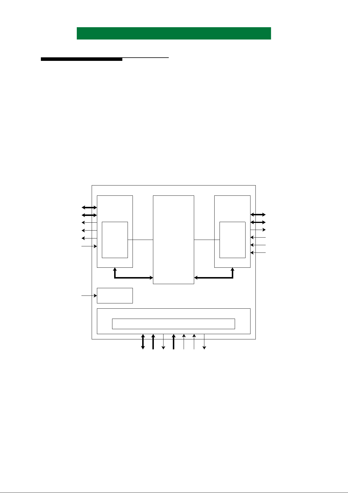
1.4 FUNCTIONAL DESCRIPTION
AHA3540 is a compression/decompression
device residing between the host interface, usually
SCSI, and the buffer manager ASIC. Major blocks
in this device are the Microproce ssor Interface, P ort
A Interface, Port B Interface, and the Compression/
Decompression Engine. The Microprocessor
Interface provides status and control information by
register access. Port A and Port B Interfaces are
configurable for polarity, handshaking modes, and
other options. The operating mode establishes the
direction of both the Port A and Port B Interfaces.
Compression or Compression P ass Through sets the
Port A Interface as an input and the Port B Interface
as an output. Conversely Decompression or
Decompression Pass Through sets the Port A
Interface as an output and the Port B Inter face as an
input. Decompression Output Disabled mode
allows the device to dec ompress a user programmed
number of records while dumping the
uncompressed data, then automatically begin
outputting the remaining uncompressed records.
A four byte Record Length register and a four
byte Record Count register allow the user to
partition the data into multiple records.
Compression Pass Through mode and
Decompression Pass Through modes allow data
transfers through the device without changing the
data. Both interfaces, Port A and Port B, have
selectable transfer modes.
Figure 1: Functional Block Diagram
PORT A
DMA
STATE
MACHINE
CLOCK
GENERATION
PORT B
DMA
STATE
MACHINE
PROCESSOR INTERFACE STATE MACHINE
PROCESSOR INTERFACE
ALDC
CORE
APARITY[1:0]
ADATA[15:0]
CLOCK
PORT A
INTERFACE
PORT B
INTERFACE
AHA3540 Compression Chip
ACOUT
ARD
BPARITY[1:0]
BDATA[15:0]
BCOUT
BCIN
MCIN[1:0]
WAITN
ADDR[4:0]
MMODE
RESETN
IREQN
AWR
ACIN
MDATA[7:0]
IBM
IBM is a registered trademark of IBM.
BWR
BRD

PS3540-1100 Page 3 of 47
Advanced Hardware Architectures, Inc.
1.4.1 PORT A AND PORT B INTERFACES
Both Port A and Port B Interfaces are
independently configurable via the Port A
Configuration register (ACNF), the Port A Polarity
register (APOL), the Port B Configuration register
(BCNF), and the Port B Polarity register (BPOL).
Port A may be configured to operate in burst mode
(20 MB/sec, Slave), 43C97C mode (40 MB /s ec,
Slave) or FAS368 mode (40 MB/sec, Slave). Port B
may be configured to operate in burst mode (20 MB/
sec, Master), 43C97C mode (40 MB/sec, Master) or
FAS368 mode (40 MB/sec, Master).
Burst mode is an asynchronous DMA transfer
mode requiring a request followed by one or more
acknowledges. Data is latched on the trailing edge
of the acknowledge pulses.
FAS368 mode is a DMA transfer mode
compatible with FAS368 devices. In this mode
DACKA (ACOUT) is asserted low for the entire
burst transfer and 16- bit data is strobed into or out of
Port A using ARD or AWR respectively. ACOUT,
A WR an d ARD must be pro grammed as ac tive low
signals in the APOL register. ACIN (DREQ) must
be programmed as active high.
Port A and Port B Interfaces both contain
sixteen-byte FIFOs.
1.4.2 DATA EXPANSION DURING
COMPRESSION
Data expansion occurs when the size of the data
increases during a compression operation. This
typically occurs when the d ata is compressed prior
to input into the chi p.The EXPAND status bit is set
if the Port B Transfer Count is larger than the Port
A T ransfer Cou nt regis ter. If data e xpansio n caused
the Port B T rans fer Count to exceed its maximum 4-
byte value then the BTC Overflow Error status gets
set. Worst case expansion allowable by the
algorithm is 12.5% or (9/8 ti mes the uncompr essed
Record Length).
1.4.3 MULTIPLE RECORDS
The AHA3540 device has two provisions to
manage compressing a block of data into multiple
records: automatic segmentation into multiple
records at the Por t A interfa ce and the Res et histor y
buffer command. During compression operation,
the Port A interface autom atically partitions the
uncompres sed data into equal length records
according to the Record Count and Record Length
registers. The two sets of registers determine the
number of records and length of each record in the
data transfer operati on. When compressing multiple
records the devi ce retains the con tents of the hist ory
buffer between records. This usually improves
compression ratio by al lowing data from the current
record to match against data from the previous
record. During decompress ion, t he previ ous re cord
must be deco mpressed prior to the current record
unless the history buffer is reset just before
compressing the curr ent record. For example, Figure
2 shows three records with a history buffer reset
before record three. In this case, record three can be
decompressed without previously decompressing
records one and two. However, decompressing
record two requires deco mpressing rec ord one first .
When processing multiple records (Record
Count is greater tha n on e), the Record Length must
be greater than 0x22.
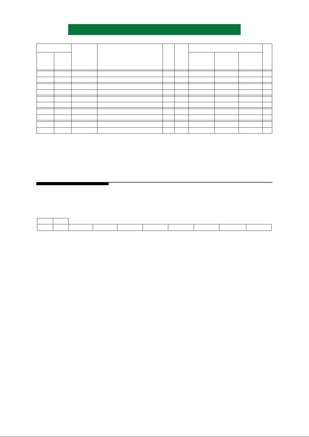
1.4.4 BYTE ALIGNMENT
Both the Port A and Port B interfaces support the
insertion and re moval of padding byte s to align data
transfers to any byte bounda ry withi n a two -byte or
four-byte wide memory system. Figure 3 shows the
four padding possibilities. In this figure, padding
bytes are designated P
i
, and normal data bytes are
designated D
i
. Four bits w ithin the command
register are used to specify the desired input and
output padding for a given command.
Pad bytes are no t counted by any of the counters.
Figure 2: Multiple Record Compression
History
Buffer Reset
Por t A
Uncompressed
Data
(optional)
RECORD 1
Compressed
History Buffer Reset
RECORD 1
Por t B
Compressed
Data
RECORD 2 RECORD 3
Compressed
RECORD 2
Compressed
RECORD 3

Page 4 of 47 PS3540-1100
Advanced Hardware Architectures, Inc.
Figure 3: Port A Interface Input Padding
2.0 COMPRESSION OPERA TION
2.1 COMPRESSION PASS THROUGH
Compression Pass Through mode allows data to
enter the Port A Interface, transfer through the ALDC
core, and exit through the Port B Interface unchanged.
Pass through mode uses the Por t A Transf er c ount er,
Port B T r ansfer counter an d R ecord Length and
Record Count re gi st e rs . The DONE status bit and
interrupt (if not masked) are set when the transfer
completes.
2.2 COMPRESSION
During compression operation, uncompressed
data flows into the Port A Interface, is compressed
by the compression engine , and the compressed data
transferre d out of the Port B Interface.
The device contains a Content Addressable
Memory (CAM). The CAM is the h istory buffer
during compression operation. The compressor
appends an end marker control code to the end of the
compressed data. It a lso pads the end of a transfer to
a byte boundary with zeroes.
The compression engine constantly monitors the
performance of compression for expansion during
compression operation. When the Port B Transfer
Count is la r ger th an t he Port A Transfe r Co un t the
EXP AND bit in the Status 0 register is set indicating
data expansion during compression operation.
Port A Interface count increments with each
byte received and when this count equals the
transfer size, all bytes in this transfer have been
received into Port A.
A compression oper ation is c omple te whe n the
last byte transfer s out of the Port B Int erface and the
Record Length is zero and the Recor d Count is one,
thus setting the DONE status bit and generating a
Done Interrupt if it is not masked.
Port A Data Transfers
ADATA
[15:8] [7:0]
D
1
n+8
n+4
n
D11D10D9D
8
D7D6D5D
4
D3D2D1D
0
D
3
D
5
D
7
D
0
D
2
D
4
D
6
Part (a): Zero Bytes of Padding
Port A Data Transfers
ADATA
[15:8] [7:0]
D
0
n+8
n+4
n
D10D9D8D
7
D6D5D4D
3
D2D1D
0
D
2
D
4
D
6
P
0
D
1
D
3
D
5
Part (b): One Byte of Padding
Port A Data Transfers
ADATA
[15:8] [7:0]
P
1
n+8
n+4
n
D9D8D7D
6
D5D4D3D
2
D1D
0
D
1
D
3
D
5
P
0
D
0
D
2
D
4
Part (c): Two Bytes of Padding
Port A Data Transfers
ADATA
[15:8] [7:0]
P
1
n+8
n+4
n
D8D7D6D
5
D4D3D2D
1
D
0
D
0
D
2
D
4
P
0
P
2
D
1
D
3
Part (d): Three Bytes of Padding
PS3540-1100 Page 5 of 47
Advanced Hardware Architectures, Inc.
3.0 DECOMPRESSION OPERATION
3.1 DECOMP RESSION P ASS THRO UGH
Decompression Pass Through mode allows data
to enter the Port B Interface, transfer through the
ALDC core, and exit through the Port A Interface
unchanged. Pass through mode uses the Port A
Transfer counter, Port B Transfer counter, Record
Length and Record Count registers. The DONE
status bit and interrupt (i f not masked) are set when
the transfer completes.
3.2 DECOMPRESSION
During Decompression mode, compressed data
flows into the Port B Interface and is decompress ed.
The resulting uncompressed data is transfer red out of
the Port A Interface.
A decompression operation is complete when
the last byt e transfers out of the Port A Interface,
thus setting the DONE status bit and generating a
Done Interrupt if it is not masked.
Decoder Control Code Errors are generated if
invalid control codes are detected in the compressed
data stream. This error is reported in the Error
Status register.
Multiple records can be decompressed by
programming the Record Count register. The
Record Count register decrements every time an
End of Record is decoded.
3.3 DECOMPRESSION OUTPUT
DISABLED MODE
Decompression output disabled mode allows
the user to program the number of records into the
Data Disable Count register to deco mpress while
discarding the output. The device then switches to
normal decompression mode and continues to
decompress the remaining records determined by
the remaining number of records in the Record
Count register , a nd trans fers thi s data out of Por t A.
4.0 MICROPROCESSOR INTER-
FACE AND REGISTER ACCESS
4.1 MICROPROCESSOR INTERFACE
Microprocessor Interface configuration is
determined by the MMODE pin. If MMODE is t ied
high, transfers are cont rolled by a chip se lect sign al
(CSN) and a read/wri te signal (RWN), if MMODE
is tied low, transfers are controlled by separate read
(READN) and write (WRITEN) signals. Re fer to
Section 10.0 Timing Specifications for timing
diagrams.
Table 1: Micropr oces so r In te rface Control Signals
4.1.1 INTERRUPTS
IREQN is th e hardware interrupt signal.
IREQN is a standard TTL output. When active, it
indicates a n interrupt is set in the devi ce. The
microprocessor can determine the cause of the
interrupt by reading the Interrupt Status register.
Masking individual interrupts with the
Interrupt Mask register disables particular
interrupts from causing the interrupt signal pin to
assert (IREQN).
The interrupt signals are reset to their inactive
state when either a hardware or software reset
occurs, new compression operation begins, or by
writing a zero to the Interrupt Status bit.
In general, the Interrupt Status and Status bits
get set even if the Interrup t Mask bits are set. The
exceptions are the One Byte at Port B, End of
Record at Port B, One Byte at Port A, and End of
Record at Port A. If these interrupt s are masked, this
status information can only be provided at the end of
transfer, not at end of records because the ALDC
core does not identify end of records in the data
stream.
PIN NAME MMODE TIED LOW MMODE TIED HIGH
MCIN[0] READN CSN
MCIN[1] WRITEN RWN
WAITN WAITN WAITN
ADDR[0]
ADDR[0] = 0 selects register bits 7:0
ADDR[0] = 1 selects register bits 15:8
ADDR[0] = 0 selects register bits 15:8
ADDR[0] = 1 selects register bits 7:0

Page 6 of 47 PS3540-1100
Advanced Hardware Architectures, Inc.
4.1.2 RESETS
There is a hardware reset signal and a software
reset. When the RESETN signal is asserted all
registers are r eset, current operat ions a re cance lled,
and the history buf fer is cleared . The so ftware reset
via the Command register does not affect the
Configuration registers (ACNF or BCNF),
Identification register (ID), the Polarity registers
(APOL or BPOL), or the Command register
(CMND). Al l other registers are reset, current
operations cancelled and the history buffer cleared.
Section 6.0 Register Description lists the
register values after a hardware reset, software reset
command, and after a transfer command.
A new transfer command doe s not reset the data
path; therefore, a hardware reset or software r eset is
generally required prior to issuing a new transfer
command.
4.1.3 PORT A INTERFACE FIFO ACCESS
It is possible to access the Port A Interface FIFO
from the microprocessor interface. T his allows the
uncompressed data stream to be altere d from the
microprocessor. This may be useful to properly
handle exception conditions. Both read and write
accesses are available. Only the Port A Interface
FIFO is accessible from the microprocessor
interface. In order to access the FIFO from th e
microprocessor interf ace, data tr ansfers on the Port
A interface must be suspended. The DMA device
attached to the Port A interface must deactivate the
DREQA line before attempting to access the FIFO
from the microprocessor interface. Unpredictable
results occ ur if DREQA is active during FIFO
access from the microprocessor interface.
Two registers are used to control access to the
FIFO: the Port A FIFO Contr ol (AFCT) register and
the Port A FIFO Data (AFIF) register. AFIF is a
two-byte register used to hold data to be written to
the Port A Interface FIFO during compression
operations and to hold data read from the Port A
Interface FIFO during decompression operations.
Two bits within AFCT are defined: Access Port A
FIFO (ACCF) and Request Port A FIFO (REQF).
The Access Port A FIFO bit must be set for the
entire duration of a read or write access to the Port A
FIFO. This bit controls whether the Port A FIFO is
accessed from the Port A interface or the
microprocessor int erface. The REQF bit is used as a
semaphore to reques t a read or a writ e to the P ort A
Interface FIFO. Read or write is determined by the
current command being executed. The FIF O can be
read only during deco mpression commands and can
be written only during compression commands.
Writing to the Port A Interface FIFO, assuming
a compression or compression bypass operation is
being executed, requires the following:
1) Suspend transfers on Port A Interface
(DREQA input must be deasserted).
2) Write a Select Port A Command.
3) Set ACCF.
4) Place data to be written to the original data
interface FIFO in AFIF.
5) Set REQF.
6) Read REQF until REQF returns to a zero.
7) Repeat steps 3 to 5 as necessary.
8) Clear ACCF and resume DMA operations.
Reading from the Port A Interface FIFO,
assuming a decompression bypass, decompression
or decompression output disabled operation is being
executed, requires the following:
1) Suspend transfers on Port A Interface
(DREQA input must be deasserted).
2) Write a Select Port A Command.
3) Set ACCF.
4) Set REQF.
5) Read REQF until REQF returns zero.
REQF is reset when two bytes have been read
from the Port A Interface FIFO and placed in
AFIF.
6) Read data from AFIF.
7) Repeat steps 3 to 5 as necessary.
8) Clear ACCF and resume DMA operations.
All Port A interface status indicators are
updated exactly as if the data is read from or written
to the Port A i nterface data bus. For instance:
• The Port A Interface Transfer Count (ATC)
will increment as b yte s are transferred th rou gh
the microprocessor interface.
• All Status bits (STAT0 and STAT1) and
Interrupt Status bits (INTS) will operate when
data is transferred through the microprocessor
interface.
• Padding bytes are supported at command
boundaries.
• Padding bytes may have to be inserted to
ensure that the last transfer from the
micropro cessor ends on an even-byte
boundary.

PS3540-1100 Page 7 of 47
Advanced Hardware Architectures, Inc.
4.2 REGISTER ACCESS
MMODE determines whet her ADDR[0] selects
even or odd addressed registers. When MMODE = 1
and ADDR[0]=0, odd addressed registers are
accessible. MMODE=1 causes ADDR[0] input
signal to be inverted.
The registers may not be stable if PAUSED is
not set. Registers should onl y be written when they
are stable.
When writing to register s th at a re de fi ned as 16bit registers, both bytes mus t be writ te n bef ore t he
register is updated. When writing t he 16-bit
Command register , t h e co mmand is e xecut ed whe n
the most significant byte is writt en. ADDR[0] selects
between the upper and lower bytes of 16-bit r egisters.
Registers i n the ALDC core require longer to
access than the external microprocessor interface
permits. Therefore, if back to back writes to the
same address ever occur, they must be separated by
a minimum of 8 clocks.
4.3 PAUSING / RESUME
When a Pause command is issued or an
unmasked data transfer interrupt occurs, the device
pauses at the next break in the DMA handshaking.
The following unmasked int errupts cause the device
to pause: ODT (Output Disable Terminated),
EORPA (End of Record at Port A), BPA (One Byte
at Port A), EORPB (End of Recor d at Port B) , BPB
(One Byte at Port B), BCMP (Port B Interface
Compare), and EORD (End of Record at Decoder).
A Slave port pauses after ACOUT (DACKA)
deasserts. For a Master port, the PAUSED status bit
will get set even if BCOUT (DREQB) is asserted.
The master port may have several transfers in its
output pipe. Therefore, several transfers could
occur before the interface pauses and DREQB
remains deasserted. Once paused and the last
transfer is complet e, the d ata bus ses ar e put i n high
impedance. Operation is continued by issuing a
resume command
Registers i n the ALDC core require longer to
access than the external microprocessor interface
permits. Therefore, these registers must be
prefetched for external reads. To assure that the
values read from these registers are current, it is
recommended that a Pause comman d be iss ued and
Paused Status read prior to reading these registers.
When a pause command is received, it takes up to
40 clock cycles to update these registers. The
PAUSED status bit is not set until the registers are
updated. Additional microprocessor accesses
during this time will delay the pre fetched reads and
Paused status. Registers that must be prefetched
include the Compressed Bytes Processed, Error
Status, Interrupt Status, Record Count and Data
Disable Count registers.
5.0 PORT A AND PORT B
CONFIGURATION
Port A and Port B are both 16-bit bidirectional
data ports with pa rity checki ng and gener ation. The
ports are controlled by the configuration registers
ACNF[15:0] and BCNF[15:0], and polarity
registers APOL[7:0] and BPOL[7:0].

Page 8 of 47 PS3540-1100
Advanced Hardware Architectures, Inc.
6.0 REGISTER DESCRIPTION
ADDR[4:0]
MNEMONIC REGISTER NAME R/W
N
O
T
E
S
REGISTER RESET VALUE P
A
G
E
#
MMODE
= 0
MMODE
= 1
HARDWARE
RESET
RESET
COMMAND
NEW
TRANSFER
COMMAND
0x00 0x01 STAT0 Stat u s , B y te 0 R 1 0x00 0x00 0x80 9
0x01 0x00 STAT1 Status, Byte 1 R 1, 4 0x0C 0x0C 0000UU00 10
0x00 0x01 ACNF0 Port A Configur a t i on, Byte 0 R/W 2 0x00 unchanged unchanged 11
0x01 0x00 ACNF1 Port A Configur a t i on, Byte 1 R/W 2 0x00 unchanged unchanged 11
0x00 0x01 BCNF0 Port B C o nfigura tion, By t e 0 R/W 3 0x00 unchanged unchanged 11
0x01 0x00 BCNF1 Port B C o nfigura tion, By t e 1 R/W 3 0x00 unchanged unchanged 12
0x02 0x03 ID0 Identification 0 R 1 0x40 0x40 0x40 12
0x03 0x02 ID1 Identification 1 R 1 0x35 0x35 0x35 12
0x02 0x03 APOL Port A P olarity R/W 2 0xFF unchanged unchanged 12
0x03 0x02 res Reserved
0x02 0x03 BPOL Port B P olarity R/W 3 0xDF unchanged unchanged 13
0x03 0x02 res Reserved
0x04 0x05 ATCH0 Port A Transfer Count, Byte 2 R 1 0x00 0x00 0x00 13
0x05 0x04 ATCH1 Port A Transfer Count, Byte 3 R 1 0x00 0x00 0x00 13
0x04 0x05
RCH0 Record Count, Byte 2 R/W 2 0x00 0x00 0x00
14
0x05 0x04 RCH1 Record Count, Byte 3 R/W 2 0x00 0x00 0x00 14
0x04 0x05 BCCH0 Port B Compare Count, Byte 2 R/W 3 0x00 0x00 0x00 14
0x05 0x04 BCCH1 Port B Compare Count, Byte 3 R/W 3 0x00 0x00 0x00 14
0x06 0x07 ATCL0 Port A Transfer Count, Byte 0 R 1 0x00 0x00 0x00 13
0x07 0x06 ATCL1 Port A Transfer Count, Byte 1 R 1 0x00 0x00 0x00 13
0x06 0x07
RCL0 Record Count, Byte 0 R/W 2 0x00 0x00
0x00 14
0x07 0x06 RCL1 Record Count, Byte 1 R/W 2 0x00 0x00
0x00
14
0x06 0x07 BCCL0 Port B Compare Count, Byte 0 R/W 3 0x00 0x00 0x00 14
0x07 0x06 BCCL1 Port B Compare Count, Byte 1 R/W 3 0x00 0x00 0x00 14
0x08 0x09 BTCH0 Port B Transfer Count, Byte 2 R 1 0x00 0x00 0x00 15
0x09 0x08 BTCH1 Port B Transfer Count, Byte 3 R 1 0x00 0x00 0x00 15
0x08 0x09
AFIF0 Por t A F IF O D at a A cc e s s, B y te 0 R/W 2 0x00 0x00 0x00
15
0x09 0x08 AFIF1 Po rt A F IF O D a ta A c c es s , By t e 1 R/W 2 0x00 0x00 0x00 15
0x08 0x09 CBPH0
Compressed Bytes Processed,
Byte 2
R 3 0x00 0x00 0x00 16
0x09 0x08
CBPH1
Compressed Bytes Processed,
Byte 3
R 3 0x00 0x00 0x00
16
0x0A 0x0B BTCL0 Port B Transfer Count, Byte 0 R 1 0x00 0x00 0x00 15
0x0B 0x0A BTCL1 Port B Transfer Count, Byte 1 R 1 0x00 0x00 0x00 15
0x0A 0x0B AFCT Po r t A F I F O Contro l R/W 2 0x00 0x00 0x00 16
0x0B 0x0A res Reserved 2
0x0A 0x0B CBPL0
Compressed Bytes Processed,
Byte 0
R 3 0x00 0x00 0x00 16
0x0B 0x0A
CBPL1
Compressed Bytes Processed,
Byte 1
R 3 0x00 0x00 0x00
16
0x0C 0x0D ERRS Err o r Status R 1 0x00 0x00 0x00 17
0x0D 0x0C res Reserved
0x0E 0x0F INTS0 Interrupt Status, Byte 0 R/W 1 0x00 0x00 0x00 17
0x0F 0x0E INTS1 Interrupt Status, Byte 1 R/W 1 0x00 0x00 0x00 18
0x10 0x11
CMND0 Command 0
R/W
0x00 0x00 0x00
19
0x11 0x10 CMND 1 C o m m a n d 1 R/W 0x00 0xA0 0x00 19
0x12 0x13
res Reserved
0x13 0x12 res Reserved
0x14 0x15 RLH0 Record L e n g th, Byte 2 R/W 0x00 0x00 unchanged 20
0x15 0x14 RLH1 Record L e n g th, Byte 3 R/W 0x00 0x00 unchanged 20
PS3540-1100 Page 9 of 47
Advanced Hardware Architectures, Inc.
Notes:
1) When CMND is not a Selection Command.
2) When CMND is a Select Port A Configuration Command.
3) When CMND is a Select Port B Configuration Command.
4) U identifies a bit that is unchanged.
6.1 STATUS 0 (STAT0)
Read Only
Hardware Reset Value = 0x00
Reset Command = 0x00
Any status bit which is active when the device pauses, due to an interrupt or Pause Command, will
remain active until t here is a Resume Command. See Appendix A.1 for dif ference s between AHA3540 an d
IBM ALDC1-20S-LP.
BUSY - Busy. This bit is set when a data transfer operation begins. It is cleared when the data transfer
operation completes successfully, when an unmasked error occurs, when a reset occurs.
PAUSED - Paused. Th is bit is set wh en a data transf er operation is currently paused. It is cleared when a
paused data transfer operation is resumed, when a reset occurs, or on a new transfer.
OUTDIS - Out put Disabled. This bit i s set when Port A Interfac e output is disabled. I t is cleared when Port
A Interface output is re-enabled, when a reset occurs, or on a new transfer.
BYP ASS - Bypass. This bit is set after a Start Compres sion Bypass or a Start Decompression Bypass
command is written to the Command register. It is cleared after a Start Compression, Start
Decompression, St art Decompression Output Disable, when a reset occurs , when an unmasked
error occurs, or when a transfer is complete.
EXP AND - Expansion. This bit i s set when the Port B Transfer Count register is larger than the Port A
Tr ansfer Count re gister . It may toggle many times d uring a compress ion operation. It is cleared
when another data transfer operation begins or when a reset occurs.
ANYINT - Any Interrupt. This bit is set while an unmasked interr upt is ac ti ve. Cl ear ed on a ne w tra nsf er,
and when all unmasked interrupts have been cleared.
ANYERR - Any Error. This bit is set when an unmasked error occurs. It is cleared when a data transfer
operation begins or when a reset occurs.
DONE - Done. This bit is set when the curr ent data transfer operatio n is complete. It is cleared when a
data transfer operation begins or when a reset occurs.
0x16 0x17 RLL0 Record Length, B y t e 0 R/W 0x00 0x00 unchanged 20
0x17 0x16 RLL1 Record Length, B y t e 1 R/W 0x00 0x00 unchanged 20
0x18 0x19 DDCH0 Data Disabled Count, Byte 2 R/W 0x00 0x00 unchanged 20
0x19 0x18 DDCH1 Data Disabled Count, Byte 3 R/W 0x00 0x00 unchanged 20
0x1A 0x1B DDCL0 Data Disabled Count, Byte 0 R/W 0x00 0x00 unchanged 20
0x1B 0x1A DDCL1 Data Disabled Count, Byte 1 R/W 0x00 0x00 unchanged 20
0x1C 0x1D EMSK Error Mask R/W 0x00 0x00 unchanged 21
0x1D 0x1C res Reserved
0x1E 0x1F IMSK0 Inter r u p t M a s k 0 R/W 0x00 0x00 unchanged 22
0x1F 0x1E IMSK1 Inte r r u p t M a s k 1 R/W 0x00 0x00 unchanged 22
MMODE =
bit7 bit6 bit5 bit4 bit3 bit2 bit1 bit0
01
0x00 0x01 BUSY PAUSED OUTDIS BYPASS EXPAND ANYINT ANYERR DONE
ADDR[4:0]
MNEMONIC REGISTER NAME R/W
N
O
T
E
S
REGISTER RESET VALUE P
A
G
E
#
MMODE
= 0
MMODE
= 1
HARDWARE
RESET
RESET
COMMAND
NEW
TRANSFER
COMMAND

Page 10 of 47 PS3540-1100
Advanced Hardware Architectures, Inc.
6.2 STATUS 1 (STAT1)
Read Only
Hardware Reset Value = 0x0C
Reset Command = 0x0C
The Status bits BPB, EORP B, BPA and EORPA will only get set after the last word i s transferr ed if the
following Interrupt Mask bits are set: BPBM, EORPBM, BPAM and EORPAM. If these bits are set, the
ALDC core provides end of transfer information, but no end of record information. See Appendix A.1 for
differences between AHA3540 and IBM ALDC1-20S-LP.
EORD - End of Record at Decoder. This bit is set when the ALDC decoder detects an End of Record
control code in the compressed data stream or when an ALDC Decoder Control Code Error
occurs. This bit is cleared af ter reset, when the de coder begins processi ng the first code word of
the next record, or when a ne w data transfer op eration begins. It i s valid for Decompre ssion and
Decompression Output Disable modes.
BCMP - Port B Interface Compare. Thi s bit is set whe n Port B T rans fer Count is gr eater than or equa l to
Port B Interface Compare Count. Othe rwise, it is cleare d. This bit is cleared af ter reset or when
a new data transfer operation begins. This bit is valid for all modes of operation.
BPB - One Byte at Port B. During com pression bypass a nd compression opera tions, this bit is set at the
same time th e End of Record at Port B (STAT1[4] and INTS1[4]) is set if only one byte at the
Port B Interface is part of the current record. During decompression bypass operation, this bit
is set during the las t da ta tra nsf er of the record at the Port B Interface if only one byte be longs
to the current r eco rd. This bit is clear ed aft er reset, when a new data t ransfer operation beg ins ,
or when the first byte of the next record is transferred. Not valid during Decompression and
Decompression Output Disable modes.
EORPB - End of Record at Por t B. During compression bypass and c ompression ope rations, t his bit i s set
when the last byte of a compressed record is transferred out of the Po rt B interface. During
decompression bypass oper ations, this bit is set when the last by te of a record is tr ansferred into
the Port B interface. This bit is cleare d after reset, when a new dat a transfer operation begins,
or when the first byte of the next record is transferred. Not valid during Decompression and
Decompression Output Disable modes.
EMPB - Empty at Port B. This bit is set when there is no data in the Port B interface data path. This bit
must be set when writing to the Recor d Lengt h register during Dec ompression bypass operat ion
and when writing to the Record Count register during Decompression and Decompression
Output disabled operations. Set after reset.
EMP A - Empty at Port A. This bit is set when there is no data in the Port A interface data path. This bit
must be set when writing to t he Reco rd Length or Record Count register s du ri ng Compr es si on
and Compression Bypass operations. S et after reset.
BP A - One Byte at Port A. During compression bypass and compression operations, this bit is set during
the last data transfer of the record at the Port A interface if only one byte belongs to the current
record. During decompression bypass, decompression, and decompression output disabled
modes, this bit is set the same time the End of Record at Port A interface bit (STAT1[0] and
INTS1[0]) is set if only one byte at the Port A interface is part of the current record. This bit is
cleared after reset, when a new data transfer operation begins, or when the first byte of the next
record is transferred.
EORP A - End of Record at Por t A. During compression by pass and compression operations, this bi t is set
each time the Record Length (RL) is decremented to zero. During decompression bypass,
decompression, and decompre ssion output disabled oper ations, this bit is set whe n the last byt e
of a record is trans ferred out the P ort A interf ace. This bit is cle ared after res et, when a new dat a
transfer operation begins, or when the first byte of the next record is transferred.
MMODE =
bit15 bit14 bit13 bit12 bit11 bit10 bit9 bit8
01
0x01 0x00 EORD BCMP BPB EORPB EMPB EMPA BPA EORPA

PS3540-1100 Page 11 of 47
Advanced Hardware Architectures, Inc.
6.3 PORT A CONFIGURATION 0 (ACNF0)
Reserved
Hardware Reset Value = 0x00
Reset Command = unchanged
6.4 PORT A CONFIGURATION 1 (ACNF1)
Read/Write
Hardware Reset Value = 0x00
Reset Command = unchanged
PARITY - Parity. When set, parity checking is enabled for the ADATA[15:0] data bus. When cleared,
parity checking is disabled for the ADATA[15:0] bus.
ODD - Odd. Setting this bit along with PARITY enables odd parity checking and generation on the
ADA TA[15:0] data bus. When cleared with P ARITY se t even parity check ing and generation is
enabled on the ADATA[15:0] data bus.
SLAVE - Slave. Must always be written with a one.
MODE[2:0]-DMA Mode. These bits conf igure the in terface DMA mode of the Por t A Interface wit h values
as defined below.
6.5 PORT B CONFIGURATION 0 (BCNF0)
Reserved
Hardware Reset Value = 0x00
Reset Command = unchanged
MMODE =
bit15 bit14 bit13 bit12 bit11 bit10 bit9 bit8
01
0x00 0x01 reserved
MMODE =
bit15 bit14 bit13 bit12 bit11 bit10 bit9 bit8
01
0x01 0x00 PARITY O DD SLAVE MODE[2:0 ] reserved
MODE[2:0] DMA TYPE
000 Reserved
001 FAS368 mode
010 43C97 ATA
011 Burst
100 Reserved
101 Reserved
110 Reserved
111 Reserved
MMODE =
bit15 bit14 bit13 bit12 bit11 bit10 bit9 bit8
01
0x00 0x01 reserved
 Loading...