


PS3520-1098
The Data Coding Leader
Advanced Hardware
Architectures
TM
Advanced Hardware
Architectures, Inc.
2365 NE Hopkins Court
Pullman, WA 99163-5601
509.334.1000
Fax: 509.334.9000
e-mail: sales@aha.com
http://www.aha.com
Product Specification
AHA3520
20 MBytes/sec ALDC Data
Compression Coprocessor IC

Advanced Hardware Architectures, Inc.
PS3520-1098
i
Table of Conte n ts
1.0 Introduction
. . . . . . . . . . . . . . . . . . . . . . . . . . . . . . . . . . . . . . . . . . . . . . . . . . . . . . . . . . . . . . . . . . . . . . . . . . . . .1
1.1 Conventions, Notations and Definitions. . . . . . . . . . . . . . . . . . . . . . . . . . . . . . . . . . . . . . . . . . . . . . . . . . . . .1
1.2 Features . . . . . . . . . . . . . . . . . . . . . . . . . . . . . . . . . . . . . . . . . . . . . . . . . . . . . . . . . . . . . . . . . . . . . . . . . . . .1
1.3 Applications. . . . . . . . . . . . . . . . . . . . . . . . . . . . . . . . . . . . . . . . . . . . . . . . . . . . . . . . . . . . . . . . . . . . . . . . . .1
1.4 Functional Description. . . . . . . . . . . . . . . . . . . . . . . . . . . . . . . . . . . . . . . . . . . . . . . . . . . . . . . . . . . . . . . . . .1
1.4.1 Port A and Port B Interfaces. . . . . . . . . . . . . . . . . . . . . . . . . . . . . . . . . . . . . . . . . . . . . . . . . . . . . . .2
1.4.2 FIFO Operation. . . . . . . . . . . . . . . . . . . . . . . . . . . . . . . . . . . . . . . . . . . . . . . . . . . . . . . . . . . . . . . . .2
1.4.3 Data Expansion During Compression . . . . . . . . . . . . . . . . . . . . . . . . . . . . . . . . . . . . . . . . . . . . . . .2
2.0 Compression Operation
. . . . . . . . . . . . . . . . . . . . . . . . . . . . . . . . . . . . . . . . . . . . . . . . . . . . . . . . . . . . . . . . . . .3
2.1 Compression Pass Through . . . . . . . . . . . . . . . . . . . . . . . . . . . . . . . . . . . . . . . . . . . . . . . . . . . . . . . . . . . . .3
2.2 Compression . . . . . . . . . . . . . . . . . . . . . . . . . . . . . . . . . . . . . . . . . . . . . . . . . . . . . . . . . . . . . . . . . . . . . . . . .3
3.0 Decompression Operation
. . . . . . . . . . . . . . . . . . . . . . . . . . . . . . . . . . . . . . . . . . . . . . . . . . . . . . . . . . . . . . . . .4
3.1 Decompression Pass Through . . . . . . . . . . . . . . . . . . . . . . . . . . . . . . . . . . . . . . . . . . . . . . . . . . . . . . . . . . .4
3.2 Decompression . . . . . . . . . . . . . . . . . . . . . . . . . . . . . . . . . . . . . . . . . . . . . . . . . . . . . . . . . . . . . . . . . . . . . . .4
3.3 Decompression Output Disabled Mode. . . . . . . . . . . . . . . . . . . . . . . . . . . . . . . . . . . . . . . . . . . . . . . . . . . . .4
4.0 Microprocessor Interface and Register Access
. . . . . . . . . . . . . . . . . . . . . . . . . . . . . . . . . . . . . . . . . . . . . . . .4
4.1 Microprocessor Interface. . . . . . . . . . . . . . . . . . . . . . . . . . . . . . . . . . . . . . . . . . . . . . . . . . . . . . . . . . . . . . . .4
4.1.1 Interrupts . . . . . . . . . . . . . . . . . . . . . . . . . . . . . . . . . . . . . . . . . . . . . . . . . . . . . . . . . . . . . . . . . . . . .4
4.1.2 Resets . . . . . . . . . . . . . . . . . . . . . . . . . . . . . . . . . . . . . . . . . . . . . . . . . . . . . . . . . . . . . . . . . . . . . . .5
4.2 Register Access. . . . . . . . . . . . . . . . . . . . . . . . . . . . . . . . . . . . . . . . . . . . . . . . . . . . . . . . . . . . . . . . . . . . . . .5
4.3 Pausing . . . . . . . . . . . . . . . . . . . . . . . . . . . . . . . . . . . . . . . . . . . . . . . . . . . . . . . . . . . . . . . . . . . . . . . . . . . . .5
5.0 Port A and Port B Configuration
. . . . . . . . . . . . . . . . . . . . . . . . . . . . . . . . . . . . . . . . . . . . . . . . . . . . . . . . . . . . .5
6.0 Register Description
. . . . . . . . . . . . . . . . . . . . . . . . . . . . . . . . . . . . . . . . . . . . . . . . . . . . . . . . . . . . . . . . . . . . . .6
6.1 Status 0 (STAT0). . . . . . . . . . . . . . . . . . . . . . . . . . . . . . . . . . . . . . . . . . . . . . . . . . . . . . . . . . . . . . . . . . . . . .7
6.2 Port A Configuration 0 (ACNF0) . . . . . . . . . . . . . . . . . . . . . . . . . . . . . . . . . . . . . . . . . . . . . . . . . . . . . . . . . .7
6.3 Port A Configuration 1 (ACNF1) . . . . . . . . . . . . . . . . . . . . . . . . . . . . . . . . . . . . . . . . . . . . . . . . . . . . . . . . . .8
6.4 Port B Configuration 0 (BCNF0) . . . . . . . . . . . . . . . . . . . . . . . . . . . . . . . . . . . . . . . . . . . . . . . . . . . . . . . . . .8
6.5 Port B Configuration 1 (BCNF1) . . . . . . . . . . . . . . . . . . . . . . . . . . . . . . . . . . . . . . . . . . . . . . . . . . . . . . . . . .9
6.6 Identification (ID). . . . . . . . . . . . . . . . . . . . . . . . . . . . . . . . . . . . . . . . . . . . . . . . . . . . . . . . . . . . . . . . . . . . . .9
6.7 Port A Polarity (APOL). . . . . . . . . . . . . . . . . . . . . . . . . . . . . . . . . . . . . . . . . . . . . . . . . . . . . . . . . . . . . . . . . .9
6.8 Port B Polarity (BPOL). . . . . . . . . . . . . . . . . . . . . . . . . . . . . . . . . . . . . . . . . . . . . . . . . . . . . . . . . . . . . . . . .10
6.9 Port A Transfer Count (ATC0, ATC1, ATC2, ATC3). . . . . . . . . . . . . . . . . . . . . . . . . . . . . . . . . . . . . . . . . .10
6.10 Port B Transfer Count (BTC0, BTC1, BTC2, BTC3). . . . . . . . . . . . . . . . . . . . . . . . . . . . . . . . . . . . . . . . . .10
6.11 Error Status (ERRS) . . . . . . . . . . . . . . . . . . . . . . . . . . . . . . . . . . . . . . . . . . . . . . . . . . . . . . . . . . . . . . . . . .1 1
6.12 Interrupt Status (INTS) . . . . . . . . . . . . . . . . . . . . . . . . . . . . . . . . . . . . . . . . . . . . . . . . . . . . . . . . . . . . . . . .11
6.13 Command (CMND) . . . . . . . . . . . . . . . . . . . . . . . . . . . . . . . . . . . . . . . . . . . . . . . . . . . . . . . . . . . . . . . . . . .12
6.14 Transfer Size (TS0, TS1, TS2, TS3). . . . . . . . . . . . . . . . . . . . . . . . . . . . . . . . . . . . . . . . . . . . . . . . . . . . . .13
6.15 Data Disabled Count (DDC0, DDC1, DDC2, DDC3). . . . . . . . . . . . . . . . . . . . . . . . . . . . . . . . . . . . . . . . . .13
6.16 error mask (EMSK) . . . . . . . . . . . . . . . . . . . . . . . . . . . . . . . . . . . . . . . . . . . . . . . . . . . . . . . . . . . . . . . . . . .14
6.17 Interrupt Mask (IMSK) . . . . . . . . . . . . . . . . . . . . . . . . . . . . . . . . . . . . . . . . . . . . . . . . . . . . . . . . . . . . . . . . .14
7.0 Signal Descriptions
. . . . . . . . . . . . . . . . . . . . . . . . . . . . . . . . . . . . . . . . . . . . . . . . . . . . . . . . . . . . . . . . . . . . . .15
7.1 Microprocessor Interface. . . . . . . . . . . . . . . . . . . . . . . . . . . . . . . . . . . . . . . . . . . . . . . . . . . . . . . . . . . . . . .15
7.2 Port A Interface . . . . . . . . . . . . . . . . . . . . . . . . . . . . . . . . . . . . . . . . . . . . . . . . . . . . . . . . . . . . . . . . . . . . . .16
7.3 Port B Interface . . . . . . . . . . . . . . . . . . . . . . . . . . . . . . . . . . . . . . . . . . . . . . . . . . . . . . . . . . . . . . . . . . . . . .17
8.0 Pinout
. . . . . . . . . . . . . . . . . . . . . . . . . . . . . . . . . . . . . . . . . . . . . . . . . . . . . . . . . . . . . . . . . . . . . . . . . . . . . . . . .1 8
9.0 Electrical Specifications
. . . . . . . . . . . . . . . . . . . . . . . . . . . . . . . . . . . . . . . . . . . . . . . . . . . . . . . . . . . . . . . . . .20
9.1 Absolute Maximum Ratings. . . . . . . . . . . . . . . . . . . . . . . . . . . . . . . . . . . . . . . . . . . . . . . . . . . . . . . . . . . . .20
9.2 Recommended Operating Conditions . . . . . . . . . . . . . . . . . . . . . . . . . . . . . . . . . . . . . . . . . . . . . . . . . . . . .20
9.3 DC Specifications . . . . . . . . . . . . . . . . . . . . . . . . . . . . . . . . . . . . . . . . . . . . . . . . . . . . . . . . . . . . . . . . . . . .20

Advanced Hardware Architectures, Inc.
ii
PS3520-1098
10.0 Timing Specifications
. . . . . . . . . . . . . . . . . . . . . . . . . . . . . . . . . . . . . . . . . . . . . . . . . . . . . . . . . . . . . . . . . . . .21
11.0 Packaging
. . . . . . . . . . . . . . . . . . . . . . . . . . . . . . . . . . . . . . . . . . . . . . . . . . . . . . . . . . . . . . . . . . . . . . . . . . . . . .34
12.0 Ordering Information
. . . . . . . . . . . . . . . . . . . . . . . . . . . . . . . . . . . . . . . . . . . . . . . . . . . . . . . . . . . . . . . . . . . . .35
12.1 Available Parts. . . . . . . . . . . . . . . . . . . . . . . . . . . . . . . . . . . . . . . . . . . . . . . . . . . . . . . . . . . . . . . . . . . . . . .35
12.2 Part Numbering . . . . . . . . . . . . . . . . . . . . . . . . . . . . . . . . . . . . . . . . . . . . . . . . . . . . . . . . . . . . . . . . . . . . . .35
13.0 AHA Related Technical Publications
. . . . . . . . . . . . . . . . . . . . . . . . . . . . . . . . . . . . . . . . . . . . . . . . . . . . . . . .35

Advanced Hardware Architectures, Inc.
PS3520-1098
iii
Figures
Figure 1: Functional Block Diagram. . . . . . . . . . . . . . . . . . . . . . . . . . . . . . . . . . . . . . . . . . . . . . . . . . . . . . . . . . . . .3
Figure 2: Pinout . . . . . . . . . . . . . . . . . . . . . . . . . . . . . . . . . . . . . . . . . . . . . . . . . . . . . . . . . . . . . . . . . . . . . . . . . . .19
Figure 3: Clock Timing . . . . . . . . . . . . . . . . . . . . . . . . . . . . . . . . . . . . . . . . . . . . . . . . . . . . . . . . . . . . . . . . . . . . . .21
Figure 4: Reset Timing. . . . . . . . . . . . . . . . . . . . . . . . . . . . . . . . . . . . . . . . . . . . . . . . . . . . . . . . . . . . . . . . . . . . . .21
Figure 5: Almost Full/Almost Empty Timing . . . . . . . . . . . . . . . . . . . . . . . . . . . . . . . . . . . . . . . . . . . . . . . . . . . . . .21
Figure 6: Processor Read Timing, MMODE = 1. . . . . . . . . . . . . . . . . . . . . . . . . . . . . . . . . . . . . . . . . . . . . . . . . . .22
Figure 7: Processor Write Timing, MMODE = 1. . . . . . . . . . . . . . . . . . . . . . . . . . . . . . . . . . . . . . . . . . . . . . . . . . .2 3
Figure 8: Processor Read Timing, MMODE = 0. . . . . . . . . . . . . . . . . . . . . . . . . . . . . . . . . . . . . . . . . . . . . . . . . . .24
Figure 9: Processor Write Timing, MMODE = 0. . . . . . . . . . . . . . . . . . . . . . . . . . . . . . . . . . . . . . . . . . . . . . . . . . .2 5
Figure 10: Port A/B Timing, Four Edge, Master Mode. . . . . . . . . . . . . . . . . . . . . . . . . . . . . . . . . . . . . . . . . . . . . . .26
Figure 11: Port A/B Timing, Four Edge, Slave Mode. . . . . . . . . . . . . . . . . . . . . . . . . . . . . . . . . . . . . . . . . . . . . . . .27
Figure 12: Port A/B Timing, Burst, Master Mode . . . . . . . . . . . . . . . . . . . . . . . . . . . . . . . . . . . . . . . . . . . . . . . . . . .28
Figure 13: Port A/B Timing, Burst, Slave Mode . . . . . . . . . . . . . . . . . . . . . . . . . . . . . . . . . . . . . . . . . . . . . . . . . . . .29
Figure 14: Peripheral Access Read Timing, MMODE = 1 . . . . . . . . . . . . . . . . . . . . . . . . . . . . . . . . . . . . . . . . . . . .30
Figure 15: Peripheral Access Write Timing, MMODE = 1 . . . . . . . . . . . . . . . . . . . . . . . . . . . . . . . . . . . . . . . . . . . .31
Figure 16: Peripheral Access Read Timing, MMODE = 0 . . . . . . . . . . . . . . . . . . . . . . . . . . . . . . . . . . . . . . . . . . . .32
Figure 17: Peripheral Access Write Timing, MMODE = 0 . . . . . . . . . . . . . . . . . . . . . . . . . . . . . . . . . . . . . . . . . . . .33
Figure 18: AHA3520 PQFP Package Specifications . . . . . . . . . . . . . . . . . . . . . . . . . . . . . . . . . . . . . . . . . . . . . . . .34

Advanced Hardware Architectures, Inc.
iv
PS3520-1098
Tables
Table 1: Microprocessor Interface Control Signals . . . . . . . . . . . . . . . . . . . . . . . . . . . . . . . . . . . . . . . . . . . . . . . . .4
Table 2: Port A Interface Signals . . . . . . . . . . . . . . . . . . . . . . . . . . . . . . . . . . . . . . . . . . . . . . . . . . . . . . . . . . . . . .5
Table 3: Port B Interface Signals . . . . . . . . . . . . . . . . . . . . . . . . . . . . . . . . . . . . . . . . . . . . . . . . . . . . . . . . . . . . . .5
Table 4: Clock Timing . . . . . . . . . . . . . . . . . . . . . . . . . . . . . . . . . . . . . . . . . . . . . . . . . . . . . . . . . . . . . . . . . . . . . .21
Table 5: Reset Timing. . . . . . . . . . . . . . . . . . . . . . . . . . . . . . . . . . . . . . . . . . . . . . . . . . . . . . . . . . . . . . . . . . . . . .21
Table 6: Almost Full/Almost Empty Timing . . . . . . . . . . . . . . . . . . . . . . . . . . . . . . . . . . . . . . . . . . . . . . . . . . . . . .21
Table 7: Processor Read Timing, MMODE = 1. . . . . . . . . . . . . . . . . . . . . . . . . . . . . . . . . . . . . . . . . . . . . . . . . . .22
Table 8: Processor Write Timing, MMODE = 1. . . . . . . . . . . . . . . . . . . . . . . . . . . . . . . . . . . . . . . . . . . . . . . . . . .2 3
Table 9: Processor Read Timing, MMODE = 0. . . . . . . . . . . . . . . . . . . . . . . . . . . . . . . . . . . . . . . . . . . . . . . . . . .24
Table 10: Processor Write Timing, MMODE = 0. . . . . . . . . . . . . . . . . . . . . . . . . . . . . . . . . . . . . . . . . . . . . . . . . . .2 5
Table 11: Port A/B Timing, Four Edge, Master Mode. . . . . . . . . . . . . . . . . . . . . . . . . . . . . . . . . . . . . . . . . . . . . . .26
Table 12: Port A/B Timing, Four Edge, Slave Mode. . . . . . . . . . . . . . . . . . . . . . . . . . . . . . . . . . . . . . . . . . . . . . . .27
Table 13: Port A/B Timing, Burst, Master Mode . . . . . . . . . . . . . . . . . . . . . . . . . . . . . . . . . . . . . . . . . . . . . . . . . . .28
Table 14: Port A/B Timing, Burst, Slave Mode . . . . . . . . . . . . . . . . . . . . . . . . . . . . . . . . . . . . . . . . . . . . . . . . . . . .29
Table 15: Peripheral Access Read Timing, MMODE = 1 . . . . . . . . . . . . . . . . . . . . . . . . . . . . . . . . . . . . . . . . . . . .30
Table 16: Peripheral Access Write Timing, MMODE = 1 . . . . . . . . . . . . . . . . . . . . . . . . . . . . . . . . . . . . . . . . . . . .31
Table 17: Peripheral Access Read Timing, MMODE = 0 . . . . . . . . . . . . . . . . . . . . . . . . . . . . . . . . . . . . . . . . . . . .32
Table 18: Peripheral Access Write Timing, MMODE = 0 . . . . . . . . . . . . . . . . . . . . . . . . . . . . . . . . . . . . . . . . . . . .33
Table 19: PQFP (Plastic Quad Flat Pack) 14 mm × 20 mm Package Dimensions. . . . . . . . . . . . . . . . . . . . . . . . .34

PS3520-1098 Page 1 of 35
Advanced Hardware Architectures, Inc.
1.0 INTRODUCTION
AHA3520 is a single chip lossless compr ession
and decompression integ rated circuit implemen ting
the industry standard adaptive lossless data
compression algorithm, al so known a s ALDC. The
device compresses, decompresses or passes
through data unchanged depending on the operat ing
mode selected. This device achieves an average
compression ratio of 2:1 on typical computer files.
The flexible hardware interface makes this part
suitable for many applicat ions.
AHA 3520 is algorithm and pi nout co mp ati bl e
to the IBM ALDC device. Compressed files
between AHA and IBM’s implementation of the
algorithm do not always produce the same
compressed code stream. However, the
decompressed results are always the same. Files
compressed on either device can be interchanged
and decompressed on either device.
Content Addressable Memory (CAM) within
the compression/decompression engine eliminates
the need for external SRAMS. This part connects
directly to industry standard peripheral chips.
Included in this specification is a functional
overview, operation modes, register descriptions,
DC and AC Electrical characteristics, ordering
information, and a listing of related technical
publications. It is intended for hardware and
software engineer s designing a compres sion system
using AHA3520.
AHA designs and develops lossless
compression, forward error correction and data
storage formatter/controller ICs. Other ALDC
product offering includes AHA3521. This is a pin
and firmware compatible device that includes
additional features. Technical publications are
available upon request.
1.1 CONVENTIONS, NOTATIONS AND
DEFINITIONS
- Active low signals have an “N” appended to the
end of the signal name. For example, CSN and
WRITEN.
- “Signal assertion” means the output signal is
logically true.
- Hex values are represented with a prefix of “0x”,
such as Register “0x00”. Binary values do not
contain a prefix, for example, MMODE = 1.
- A prefix or suffix of “x” indicates a letter missing
in a register name or signal name. For example,
xCNF0 refers to the ACNF0 or BCNF0 register.
- A range of signal names or register bits is denoted
by a set of colons between the numbers. Most
significant bit is always shown first, followed by
least significant bit. For example, MDATA[7:0]
indicates signal names MDATA7 through
MDATA0.
- Mega Bytes per second is referred to as MBytes/
sec or MB/sec.
- Reserved bits in registers are referred as “
res
”.
1.2 FEATURES
PERFORMANCE:
• 20 MB/s data compression, decompression or
pass-through rate with a single 40 MHz clock
• 2:1 average compression ratio
• A four byte
Transfer Size
register allows block
transfers up to 4 gigabytes
• Error checking in decompression mode
reportable via an interrupt
FLEXIBILITY:
• In-line and Look-aside architectures supported
• Polled or interrupt driven I/O
• T wo independent DMA ports programma ble for 8
or 16-bit transfers, handshaking modes and
master or slave operation
• Programmable polarity for DMA control signals
SYSTEM INTERFACE:
• Single chip data compression solution
• Two selectable microprocessor interfaces
• Programmable Interrupts
• Interfaces directly with the AHA5140 tape
formatter and industry standard SCSI chips
OTHERS:
• Open standard ALDC adaptive lossless
compression algorithm
• Complies to QIC-154, ECMA 222, ANSI
X3.280-1996 and ISO 15200 standard
specifications
• Compatible to IBM ALDC1-20S-HA
specification
• 100 pin package in 14 × 20 mm PQFP
1.3 APPLICATIONS
• QIC or 8 mm tape drives
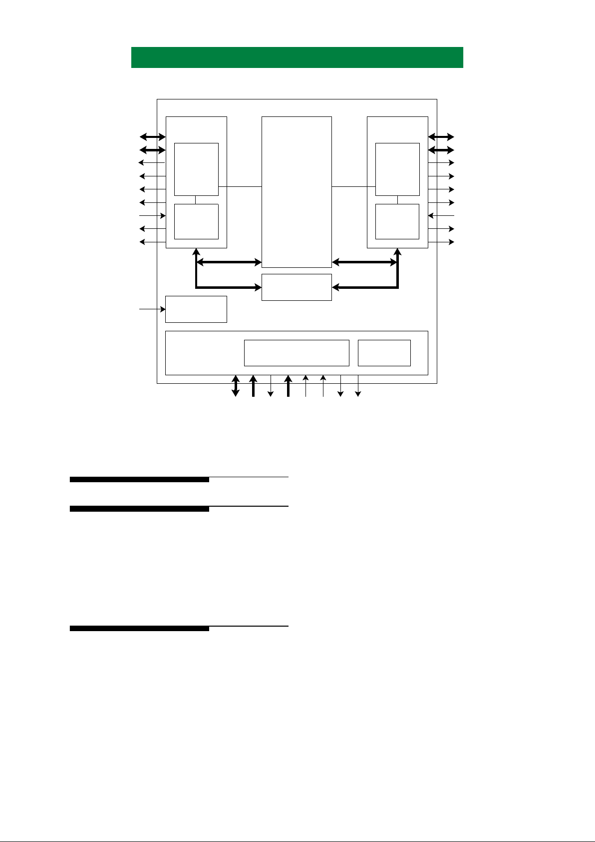
1.4 FUNCTIONAL DESCRIPTION
AHA3520 is a compression/decompression
device residing between the host interface, usually
SCSI, and the buffer manager ASIC. Major blocks
in this device are the Micropr ocessor Interfac e, Port
A Interface, Port B Interface, and the Compression /
Decompression Engine. The Micropro cessor
Interface provides status and control information by
register access. Port A and Port B Interfaces are
DMA ports configurable for bus width, polarity,
handshaking modes, and other options. The

Page 2 of 35 PS3520-1098
Advanced Hardware Architectures, Inc.
operating mode establishe s the direction of both the
Port A and Port B Interfaces. Compression or
Compression Pass Through sets the Port A Interface
as an input and the Port B Interface as an output.
Conversely Decompression or Decompression Pass
Through sets the Port A Interface as an output and
the Port B Interface as an input. Decompression
Output Disabled mode allows the device to
decompress a block of data up to a predetermined
point while dumping the uncompressed data, then
automatically begin outputting the remaining
uncompressed data in that block or record.
A four byte Tr ansfer Size counter allows the use r
to partition the data into bl ocks of four gigabytes or
less to process. Compression Pas s Through mode and
Decompression Pass Through modes al low data
transfers through the devi ce wi thout cha nging the
data. Both the Port A Interfac e and Po rt B I nte rface
have a 16-byte FIFO with Almost Empty and Almost
Full signal pins and progr ammable t hre shol ds. Bot h
DMA interfaces, Port A and Port B, have
programmable wait states in add it ion t o fou r
selectable DMA transfer modes: a synch ronou s
request/acknowledge pair , asynchronous burst mode,
and two peripheral acces s modes t hat correlate with
the two microprocesso r modes.
1.4.1 PORT A AND PORT B INTERFACES
Both Port A and Port B Interfaces are
independently configurable via the
Port A
Configuration
registers (ACNFx), the
Port A
Polarity
register (APOL), the
Port B Configuration
registers (BCNFx), and the
Port B Polarity
register
(BPOL). Both operate in four DMA modes.
Four-edge mode is an asynchronous dat a transfer
requiring a request and ackn owledge pul se f or each
transfer of one or two bytes, depending on th e width
configuration of the Inte rfa ce. A f our e dge transfer
begins by asserting the request signal, followed by
the acknowledge in response to t he r eque st, whi ch
causes the request to dea ssert, and final ly this causes
the acknowledge to deassert. Dat a i s tr ans fer red o n
the trailing edge of the a cknowl edge s igna l.
Burst mode is similar to four -edge mode except
there may be many acknowledges whil e the request
is held asser ted . Th e advantage of this mode i s that
it requires fewer clocks per transfer.
Two peripheral access modes exist and are
selected via the MMODE pin. Peripheral access
allows the microprocessor to write to and read from
a peripheral device connected to the Port A
Interface or P ort B Interface. This mode is a
relatively slow , asynchronous transfer. This mode is
not allowed during a data transfer operation.
1.4.2 FIFO OPERATION
Port A and Port B Interfaces both contain
sixteen-byte FIFOs with progr ammable th resholds.
AHA3520 has an Almost Full and an Almos t Empty
signal pin associated with each of the Data
Interfaces. The FIFO thres holds are programmed in
the configuration regist ers (ACNF0 and BCNF0). If
the Data Interface is configured for either four-edge
or burst mode of operation the FIFO threshold
determines when request gets asserted and
deasserted. During an output transfer the request
signal asserts when the number of bytes in the FIFO
is greater than or equal to the programmed FIFO
threshold. The interface continues to request data
transfers until the FIFO becomes empty.
When transferring data into either the Port A or
Port B Interfaces, the request signal asserts when
the number of empty byte locations in the FIFO is
greater than or equal to the programmed FIFO
threshold. The interface continues to request data
transfers until the FIFO is full.
The almost full (xAF) and almost empty (xAE)
signals are always ava ilable to the user . Almost Ful l
can be used as an early warning indicator to stop
transferring d ata i nto th e Po rt B I nterf ace or Po rt A
Interface. The xAE signal can be used to stop
transfers out of the Port A Interface or Port B
Interface
The xAF signal deasserts when a transfer
operation begins. It asserts the clock after the
number of empty byte locat ions in the FIFO is less
than or equal to the FIFO thre shold. The xAF s ignal
deasserts the clock after the number of empty byte
locations in the FIFO is greater than the FIFO
threshold.
The xAE signal asserts when a transfer
operation begins. It deasserts the clock after the
number of available bytes in the FIFO is greater than
the FIFO threshold. The xAE signal asserts after the
clock when the number of available bytes in the
FIFO is less than or equal to the FIFO threshold.
1.4.3 DATA EXPANSION DURING
COMPRESSION
Data expansion occurs when the size of the data
increases during a compressi on oper at ion. Th is
typically occurs when t he data is compressed prior to
input into the chip.The EXPAND status bit is set if
the Port B Trans fer Count is lar ger than th e
Tr ansfer
Size
register. If data expansion caused the Port B
Transfer Count t o ex ceed it s maximum 4-byte value
then the BTC Overflow Error status get s set . Worst
case expansion allowable by the algorithm is 12.5%
or (9/8 times the uncompressed t ran sfe r si ze) .
PS3520-1098 Page 3 of 35
Advanced Hardware Architectures, Inc.
Figure 1: Functional Block Diagram
2.0 COMPRESSION OPERATION
2.1 COMPRESSION PASS THROUGH
Compression Pass Through mode allows data to
enter the Port A Interface, transfer through the device
unchanged and exit through the Port B Interface. Pass
through mode uses the Port A Transfer counter, Port
B Trans f er c ounter and
Transfer Size
register. The
DONE status bit and i nterrup t (if not mask ed) are se t
when the tran sf er c ompletes.
2.2 COMPRESSION
During compression operation, uncompressed
data flows into the Port A Interface, is compressed
by the compression engin e and the compressed dat a
transferred out of the Port B Interface.
The device contains a Content Addressable
Memory (CAM). The CAM is the history buffer
during compression operation. The compressor
appends an end marker control code to the end of the
compressed data. It also pads the end of a transfer t o a
byte boundary with zeroes. End marker control
codewords are monitored during decompression, to
determine Decompression End errors.
The compression engine constantly monitors
the performance of compression for expansion
during compression operat ion. The EXPAND bit is
set if the Port B Transfer Count is larger than the
transfer size at the end of a compressi on o peration.
When the Port B Transfer Count is higher than the
Port A Transfer Count the EXPAND bit in the
Status 0
register is set indicating data expansion
during compression operation.
Port A Interface count increments with each
byte received and when this count equals the
transfer size, all bytes in this transfer have been
received into Port A.
A compression operati on is c omplete when t he
last byte transfer s out of the Port B Int erface and the
Port B Interface count is zero, thus setting the
DONE status bit and generati ng a Done Inter rupt if
it is not masked.
PORT B
TRANSFER
COUNTER
PORT A
DMA
STATE
PORT A
TRANSFER
COUNTER
MACHINE
CLOCK
GENERATION
PORT B
DMA
STATE
MACHINE
INTERRUPT
LOGIC
PROCESSOR INTERFACE
STATE MACHINE
PASS THROUGH
CONTROLLER
PROCESSOR
INTERFACE
ALDC
ENGINE
APARITY[1:0]
ADATA[15:0]
CLOCK
MDATA[7:0]
PORT A
INTERFACE
PORT B
INTERFACE
AHA3520 Compression Chip
ACOUT
ARD
APCS
AAF
BPARITY[1:0]
BDATA[15:0]
BCOUT
BCIN
BPCS
BAF
MCIN[1:0]
WAITN
ADDR[4:0]
MMODE
RESETN
IREQN
IREQ
AWR
ACIN
AAE
BAE
BRD
BWR

Page 4 of 35 PS3520-1098
Advanced Hardware Architectures, Inc.
3.0 DECOMPRESSION OPERATION
3.1 DECOMPRESSIO N PAS S THROU GH
Decompression Pass Through mode allows data
to enter the Port B Interface, transfer through the
device unchanged and exit through the Port A
Interface. Pass through mode uses the Port A Transfer
counter, Port B Transfer counter and
Transfer Size
register. The DONE status bit and interrupt (if not
masked) are set when the transfer completes.
3.2 DECOMPRESSION
During Decompression mode, compressed data
flows into the Port B Interface and is decompress ed.
The resulting uncompressed data is transfer red out of
the Port A Interface.
The number of compressed bytes in the transfer
is programmed into the four byte
Transfer Size
register. A decompression operation is complete
when the last byte transfers out of the Po rt A
Interface, thus setting the DONE status bit and
generating a Done Interrupt if it is not maske d.
Two types of errors are detected and reported
during decompression. Decoder Control Coder
Errors are caused by detection of invalid control
codes in the compress ed data stream. Decoder End
Errors are detected when either the decompressor
encountered an end control code before the
expected end of record indicated by the
Transfer
Size
register, or the end of record was reached
according to the
Transfer Size
register but no end
control code was detected. The se errors are reported
in the
Error Status
register.
3.3 DECOMPRESSION OUTPUT
DISABLED MODE
Decompressed output disabl ed mode allows the
user to decompress to a point in the record or bl ock
and rebuild the history buffer while discarding the
uncompresse d data. After the point in the file is
reached where the user wants the data (Port A
Transfer Count is equal or greater than the Data
Disable Count), the device switches to normal
decompression mode and th e rema inder of that fi le
is decompressed and transferred out of the Port A
Interface. Removal of CBG hea der s also applies to
this mode.
4.0 MICROPR OCESSOR INTERFACE AND REGISTER ACCESS
4.1 MICROPROCESSOR INTERFACE
Microprocessor Interface configuration is
determined by the MMODE pin. If MMODE is t ied
high transfers are controlled by a chip sele ct si gnal
(CSN) and a read/write signal (RWN), otherwise
transfers are controll ed by separate read (READN),
write (WRITEN) signals. Refer to Section 10.0
Timing Specifications
for timing diagrams.
4.1.1 INTERRUPTS
IREQ and IREQN are two hardware interrupt
signals. IREQN is a negative active open-drain
output that requires a pull-up resistor if it is used.
IREQ is a standard TTL output. When active they
indicate an interrupt is set in the device. The
microprocessor can determine the cau se of the
interrupt by reading the
Interrupt Status
register.
Masking individual interrupts with the
Interrupt Mask
register disables particular
interrupts from causing the interrupt signal pins to
assert (IREQ and IREQN). Th ey do not disa ble bits
in the
Interrupt Status
register.
The interrupt signals are reset to their inactive
state when either a hardware or software reset
occurs, when a data transfer operation resumes, or
when a data transfer operation begins. In addition,
disabling Interrup t Mas k bit s aft er the In terr upt pi n
is asserted, clears the interrupt and deasserts the
Interrupt pin.
Table 1: Microprocessor Interface Control Signals
PIN NAME MMODE TIED LOW MMODE TIED HIGH
MCIN[0] READN CSN
MCIN[1] WRITEN RWN
WAITN WAITN WAITN
ADDR[0]
ADDR[0] = 0 selects register bits 7:0
ADDR[0] = 1 selects register bits 15:8
ADDR[0] = 0 selects register bits 15:8
ADDR[0] = 1 selects register bits 7:0
PS3520-1098 Page 5 of 35
Advanced Hardware Architectures, Inc.
4.1.2 RESETS
The AHA3520 has one hardware reset signal
and a software reset. When the RESETN signal is
asserted all registers except the
Identification
registers are r eset, current oper ations a re cance lled,
and the history buf fer is cleared . The s oftware reset
via the
Command
register does not affect the
Configuration
registers (ACNFx or BCNFx),
Identification
registers (IDx), either of the
Polarity
registers (APOL or BPOL), or the
Command
register (CMND). All other registers are reset,
current operations cancelled and the history buffer
cleared.
4.2 REGISTER ACCESS
MMODE determines whether ADDR[0]
selects even or odd addressed registers. When
MMODE is high and ADDR[0]=0, odd addressed
registers are accessible. MMODE=1 causes
ADDR[0] input signal to be inverted.
The following registers may not be stable if
BUSY is set:
Status 0, Status 1, Port A Transfer
Count, Port B Transfer Count, Error Status
,
Interrupt Status
and
FIFO Access
.
4.3 PAUSING
When a Pause command is issued, the device
pauses at the next break in the DMA handshaking.
When a port is in slave mode, it pauses after
xCOUT (DACKx) deasserts. When a port is in
master mode and xCOUT (DREQx) is asserted, the
port does not pause until xCIN (DACKx) is
recieved from the external DMA device. The
AHA3520 waits until both ports are paused, at
which time the BUSY status bit clears and the
PAUSED status bit and interrupt are set.
5.0 PORT A AND PORT B
CONFIGURATION
Port A and Po rt B operate identically. They
both are 16-bit bidirectional data ports with parity
checking and generation. There are three
configuration registers associated with each port
and a polarity register that determines the polarity
of all of the control signals for that port.
The function of the contro l pin is determined by
either xCNF0[13, 12] bits or
Command
register
programmed for peripheral access. The polarity of
control signals are c ontro lled b y s pecif ic bit s in the
Polarity
registers.
Table 2: Port A Interface Signals
Table 3: Port B Interface Signals
SIGNAL
NAME
MASTER
SLAVE=0
SLAVE
SLAVE=1
APOL
bit
DIRECTION
ACIN DACKA DREQA 7 I
ACOUT DREQA DACKA 5 O
AWR deasserted AWR 4 O
ARD d easserted ARD 3 O
APCS APCS APCS 2 O
AAF AAF AAF 1 O
AAE AAE AAE 0 O
SIGNAL
NAME
MASTER
SLAVE=0
SLAVE
SLAVE=1
BPOL
bit
DIRECTION
BCIN DACKB DREQB 7 I
BCOUT DREQB DACKB 5 O
BWR deasserted BWR 4 O
BRD deasserted BRD 3 O
BPCS BPCS BPCS 2 O
BAF BAF BAF 1 O
BAE BAE BAE 0 O

Page 6 of 35 PS3520-1098
Advanced Hardware Architectures, Inc.
6.0 REGISTER DESCRIPTION
Notes:
1) When CMND is not a Selection Command.
2) When CMND is a Select Port A Configuration Command.
3) When CMND is a Select Port B Configuration Command.
4) When CMND is any Transfer Command or Select Port A Configuration Command.
5) When CMND is any Transfer Command or Select Port B Configuration Command.
ADDR[4:0]
MNEMONIC REGISTER NAME R/W NOTES
REGISTER RESET VALUE
MMODE=0 MMODE=1
HARDWARE
RESET
RESET
COMMAND
NEW
TRANSFER
COMMAND
0x00 0x01 STAT0 Stat us 0 R 1 0x00 0x00 0x80
0x01 0x00
res Reserved
0x00 0x01 ACNF0 Por t A Confi g u ration 0 R/W 2 0x00 unchanged unchanged
0x01 0x00 ACNF1 Por t A Confi g u ration 1 R/W 2 0x00 unchanged unchanged
0x00 0x01 BCNF0 Port B C o n f igura tion 0 R/W 3 0x00 unchanged unchanged
0x01 0x00 BCNF1 Port B C o n f igura tion 1 R/W 3 0x00 unchanged unchanged
0x02 0x03 ID Identificati on R 1 0xC1 0xC1 0xC1
0x03 0x02
res Reserved
0x02 0x03 APOL Port A P o l a rity R/W 2 0xFF unchanged unchanged
0x03 0x02
res Reserved
0x02 0x03 BPOL Port B Po l arity R/W 3 0xFF unchanged unchanged
0x03 0x02
res Reserved
0x04 0x05 A TC2 Port A Transfer Count, Byte 2 R 4 0x00 0x00 0x00
0x05 0x04 A TC3 Port A Transfer Count, Byte 3 R 4 0x00 0x00 0x00
0x06 0x07 A TC0 Port A Transfer Count, Byte 0 R 4 0x00 0x00 0x00
0x07 0x06 A TC1 Port A Transfer Count, Byte 1 R 4 0x00 0x00 0x00
0x08 0x09 BTC2 Port B Transfer Count, Byte 2 R 5 0x00 0x00 0x00
0x09 0x08 BTC3 Port B Transfer Count, Byte 3 R 5 0x00 0x00 0x00
0x0A 0x0B BTC0 Port B Transfer Count, Byte 0 R 5 0x00 0x00 0x00
0x0B 0x0A BTC1 Port B Transfer Count , Byte 1 R 5 0x00 0x00 0x00
0x0C 0x0D ERRS Er r o r S tatus R 1 0x00 0x00 0x00
0x0D 0x0C
res Reserved
1
0x0E 0x0F INTS Inte r r u p t S tatus R 1 0x00 0x00 0x00
0x0F 0x0E
res Reserved
0x10 0x11
res Reserved
0x11 0x10 CMND Command R/W 0x00 0x00 0x00
0x12 0x13
res Reserved
0x13 0x12
res Reserved
0x14 0x15 TS2 Tra n s f e r Size , B y te 2 R/W 0x00 0x00 unchanged
0x15 0x14 TS3 Tra n s f e r Size , B y te 3 R/W 0x00 0x00 unchanged
0x16 0x17 TS0 Tra n s f e r Size , B y te 0 R/W 0x00 0x00 unchanged
0x17 0x16 TS1 Tra n s f e r Size , B y te 1 R/W 0x00 0x00 unchanged
0x18 0x19 DDC2 Data Disabled Count, Byte 2 R/W 0x00 0x00 unchanged
0x19 0x18 DDC3 Data Disabled Count, Byte 3 R/W 0x00 0x00 unchanged
0x1A 0x1B DDC0 Data Disabled Count, Byte 0 R/W 0x00 0x00 unchanged
0x1B 0x1A DDC1 Data Disabled Count, Byte 1 R/W 0x00 0x00 unchanged
0x1C 0x1D EMSK Err o r M a s k R/W 0x00 0x00 unchanged
0x1D 0x1C
res Reserved
0x1E 0x1F IMSK Inte r ru pt Mas k R/W 0x00 0x00 unchanged
0x1F 0x1E
res Reserved

PS3520-1098 Page 7 of 35
Advanced Hardware Architectures, Inc.
6.1 STATUS 0 (STAT0)
Read Only
Reset Value = 0x00
Software Reset Value = 0x00
BUSY - Busy. This bit is set when a data transfer operation begins. It is cleared when the data transfer
operation completes successfully, when an unmasked error occurs, when a reset occurs, or
when a paused command is issued by the microprocessor.
PAUSED - Paused. This bit is set when a data transfer operation is currently paused. It is cleared when a
paused dat a transfer operation is resum ed or when a reset occurs.
OUTDIS - Output Disabled. This bit i s set when Port A Interfac e output is disabled. I t is cleared when Port
A Interface output is re-enabled or when a reset occurs.
BYP ASS - Bypass. This bit is set after a Start Compression Bypass or a Start Decompression Bypass
command is written to the
Command
register. It is cleared after a Start Compression, Start
Decompression or when a reset occurs.
EXP AND - Expansion. This bit is set when the
Port B Transfer Count
register is larger than the
Transfer
Size
register at the end of a compression operation. It is cleared when another data transfer
operation begins or when a reset occurs.
ANYINT - Any Interrupt. This bit is set while an unmasked interrupt is active. This signal mirrors the
Interrupt signal pin.
ANYERR - Any Error. This bit is set when an unmasked error occurs. It is cleared when a data transfer
operation begins or when a reset occurs.
DONE - Done. This bit is set when the current data transfer operation is complete. It is cleared when a
data transfer operation begins or when a reset occurs.
6.2 PORT A CONFIGURATION 0 (ACNF0)
Read/Write
Reset Value = 0x00
Software Reset Value = unchanged
WAITST[2:0]-Wait State. These bits configure the number of wait states used during a Port A Interface
peripheral access. The values 011 through 111 are valid.
FIFOTH[3:0]-FIFO Threshold. These bits configure the Port A FIFO threshold value. Values from 0000
through 1111 are valid.
MMODE =
bit7 bit6 bit5 bit4 bit3 bit2 bit1 bit0
01
0x00 0x01 BUSY PAUSED OUTDIS BYP ASS EXPAND ANYINT ANYERR DONE
MMODE =
bit7 bit6 bit5 bit4 bit3 bit2 bit1 bit0
01
0x00 0x01 reserved WAITST[2:0] FIFOTH[3:0]

Page 8 of 35 PS3520-1098
Advanced Hardware Architectures, Inc.
6.3 PORT A CONFIGURATION 1 (ACNF1)
Read/Write
Reset Value = 0x00
Software Reset Value = unchanged
PARITY - Parity. When set, parity checking is enabled for the ADATA[15:0] data bus. When cleared,
parity checking is disabled for the ADATA[15:0] bus.
ODD - Odd. Setting this bit along with PARITY enables odd parity checking and generation on the
ADA TA[15:0] data bus. When cleared with PARITY set even parity checking and generation i s
enabled on the ADATA[15:0] data bus.
SLAVE - Slave. When set, the Port B Interface acts as a slave device and generates acknowledges in
response to requests. When cleared, the Port B Interface acts as a DMA master, and generates
requests and expects acknowledges.
MODE[1:0]-DMA Mode. These bits configure th e interface DMA mode of t he Port A Interfac e with values
as defined below.
WIDE - Two Byte. When set, ADATA[15:0] and PARITY[1:0] are used. When cleared, AD[7:0] and
PARITY[0] are used.
6.4 PORT B CONFIGURATION 0 (BCNF0)
Read/Write
Reset Value = 0x00
Software Reset Value = unchanged
WAITST[2:0]-Wait State. These bits configure the number of wait states used during Port A Interface
peripheral access. The values 001 thr ough 11 1 are v alid. Values 000, 001, 010 result in two wait
states.
FIFOTH[3:0]-FIFO Threshold. These bits configure the Port A FIFO threshold value. Values from 0001
through 1111 are valid. A value of 0000 results in the same operation as 0001.
MMODE =
bit7 bit6 bit5 bit4 bit3 bit2 bit1 bit0
01
0x01 0x00 PARITY ODD SLA VE MODE[1:0] WIDE reserved
MODE[1:0] DMA TYPE
00 Four Edge
01 Burst
10 reserved
11 reserved
MMODE =
bit7 bit6 bit5 bit4 bit3 bit2 bit1 bit0
01
0x00 0x01 reserved WAITST[2:0] FIFOTH[3:0]

PS3520-1098 Page 9 of 35
Advanced Hardware Architectures, Inc.
6.5 PORT B CONFIGURATION 1 (BCNF1)
Read/Write
Reset Value = 0x00
Software Reset Value = unchanged
PARITY - Parity. When set, parity checking is enabled for the BDATA[15:0] data bus. When cleared,
parity checking is disabled for the BDATA[15:0] bus.
ODD - Odd. When set, odd parity checking and generation is used on the BDATA[15:0] data bus.
When cleared, even parity checking and generation is used on the BDATA[15:0] data bus.
SLAVE - Slave. When set, the Port B Interface acts as a slave device and generates acknowledges in
response to requests. When cleared, the Port B Interface acts as a DMA master, and generates
requests and expects acknowledges.
MODE[1:0]-DMA Mode. These bits configure the in terface DMA mod e of the Port B Interf ace with values
as defined below.
WIDE - Two Byte. When set, BDATA[15:0] and PARITY[1:0] are used. When cleared, BD[7:0] and
PARITY[0] are used.
6.6 IDENTIFICATION (ID)
Read Only
Value = Contact AHA Applications Engineering
ID[7:0]- The bits of this register correspond to the identification code of the chip. This register is
accessible when CMND is not a Selection Command.
6.7 PORT A POLARITY (APOL)
Read/Write
Reset Value = 0xFF
Software Reset Value = unchanged
The bits of this register correspond to Port A Interface signals. A set bit programs the corresponding
signal to be active low. A cleared bit programs the corresponding signal to be active high. This register is
only accessible when CMND is Select Port A Configuration.
MMODE =
bit7 bit6 bit5 bit4 bit3 bit2 bit1 bit0
01
0x01 0x00 PARITY ODD SLA VE MODE[1:0] WIDE reserved
MODE[1:0] DMA TYPE
00 Four Edge
01 Burst
10 reserved
11 reserved
MMODE =
bit7 bit6 bit5 bit4 bit3 bit2 bit1 bit0
01
0x02 0x03 ID[7:0]
MMODE =
bit7 bit6 bit5 bit4 bit3 bit2 bit1 bit0
01
0x02 0x03 ACIN reserved ACOUT A WR ARD APCS AAF AAE

Page 10 of 35 PS3520-1098
Advanced Hardware Architectures, Inc.
6.8 PORT B POLARITY (BPOL)
Read/Write
Reset Value = 0xFF
Software Reset Value = unchanged
The bits of this register correspond to Port B Interface signals. A set bit programs the corresponding
signal to be active low. A cleared bit programs the corresponding signal to be active high.This register is
only accessible when CMND is Select Port B Configuration.
6.9 POR T A TRANSFER COUNT (ATC0, ATC1, ATC2, ATC3)
Read Only
Reset Value = 0x00
Software Reset Value = 0x00
A TC[31:0]-Port A Transfer Count. These regi ste rs p rovi de st at us i nfor ma ti on on t he number of b ytes
transferred for a curre nt da ta t ra nsfe r ope rat ion . Du rin g a compr ession operation, ATC is
incremented as each orig inal data byt e is re ceived by the Port A Inte rface. W hen ATC equals TS
during compression, all bytes in the compress ion operation have been receive d by the AHA3520.
During a decompression operation, ATC is incremented as each decompressed data byte is sent by
the Port A Interface. This register is only accessible when CMND is not a Sele cti on Command.
6.10 PORT B TRANSFER COUNT (BTC0, BTC1, BTC2, BTC3)
Read Only
Reset Value = 0x00
Software Reset Value = 0x00
BTC[31:0] -Port B Transfer Count. These registers provide status information on the number of bytes
transferred for a current data transfer operation. During a compression operation, BTC is
incremented as each compressed data byte is sent by the Port B Interface. During a
decompression operati on, BTC is incremen ted as each compressed data byte is recei ved by the
Port B Interface. When BTC equals TS during decompression, all bytes in the decompression
operation have been received by the AHA3520 host interface.This register is only accessible
when CMND is not a Selection Command.
MMODE =
bit7 bit6 bit5 bit4 bit3 bit2 bit1 bit0
01
0x02 0x03 BCIN reserved BCOUT BWR BRD BPCS BAF BAE
MMODE =
bit7 bit6 bit5 bit4 bit3 bit2 bit1 bit0
01
0x06 0x07 ATC[7:0]
0x07 0x06 ATC[15:8]
0x04 0x05 ATC[23:16]
0x05 0x04 ATC[31:24]
MMODE =
bit7 bit6 bit5 bit4 bit3 bit2 bit1 bit0
01
0x00 0x01 BTC[7:0]
0x01 0x00 BTC[15:8]
0x00 0x01 BTC[23:16]
0x01 0x00 BTC[31:24]

PS3520-1098 Page 11 of 35
Advanced Hardware Architectures, Inc.
6.11 ERROR STATUS (ERRS)
Read Only
Reset Value = 0x00
Software Reset Value = 0x00
The
Error Status
register provides error status bi ts to the micr oprocessor. This register should only be read
when CMND is not a Selection Command. These bits are set regardless of the error mask settings .
APERR - Port A Interface Parity Error . This bit is set when a pa rity er ror is det ected during a transfer into
ADATA[15:0] and the Port A Interface Parity bit is set. It is cleared when a data transfer
operation begins or when a reset occurs.
BPERR - Port B Interface Pari ty Error. This bit is se t when a pari ty error is detected dur ing a transf er into
BDATA[15:0] and the Port B Interface Parity bit is set. It is cleared when a data transfer
operation begins or when a reset occurs.
BTCO - Port B Transfer Count Overflow Error. This bit is set when a carry out is detected on the
Port B
Tr ansfer Count
register. It is cleared when a data transfer operation begins or when a reset occurs.
ATCO - Port A Transfer Count Overflow Error. This bit is set when a carry out is detected on the
Port A
Tr ansfer Count
register. It is cleared when a data transfer operation begins or when a reset occurs.
ADCC - ALDC Decoder Control Code Error. This bit is set during decompression when an invalid
control code is detected in the compressed data stream. It is cleared when a data transfer
operation begins or when a reset occurs.
ADE - ALDC Decoder End Error. This bit is set during decompression when an End control code is
detected while Port B T r ansfer Cou nt is less t han T ransf er Size or when BTC equa ls TS and no
End control code is detected in the compressed data stream. It is cleared when a data transfer
operation begins or when a reset occurs.
6.12 INTERRUPT STATUS (INTS)
Read Only
Reset Value = 0x00
Software Reset Value = 0x00
DONE - Done Interrupt. This bit is set when data transfer has completed on the Po rt B I nte rf ace during
compression and when data transfer has completed on the Port A Interface during
decompression. It is cleared when a data transfer operation begins or when a reset occurs.
PAUSED - Paused Interrupt. This bit is set when the current tr ansfer st ep after t he microproc essor issu es a
Pause command is completed. It is cleared when the microprocessor issues a Resume
command, when a data transfer operation begins, or when a reset occurs.
ERROR - Error Interrupt. This bit is set when an error occurs. It is cleared when a data transfer operation
begins or when a reset occurs. The
Error Status
register is used to determine the cause of t he error .
MMODE =
bit7 bit6 bit5 bit4 bit3 bit2 bit1 bit0
01
0x0C 0x0D reserved APERR BPERR reserved BTCO A TCO ADCC ADE
MMODE =
bit7 bit6 bit5 bit4 bit3 bit2 bit1 bit0
01
0x0E 0x0F DONE PAUSED re served ERROR

Page 12 of 35 PS3520-1098
Advanced Hardware Architectures, Inc.
6.13 COMMAND (CMND)
Read/Write
Reset Value = 0x00
Software Reset Value = 0x00
The
Command
register is used to program the operation of the compres sion sub system.
CMND[7:0]-Command.This register provides for operation as described in the following table.
MMODE =
bit7 bit6 bit5 bit4 bit3 bit2 bit1 bit0
01
0x11 0x10 CMND[7:0]
CMND[7:0] ACTION
SELECTION COMMANDS
0xC1
Select Port A Configuration. The
Port A Configuration
and
Port A Polarity
registers are enabled for reads and writes.
0xC2
Select Port B Configuration. The
Port B Configuration
and
Port B Polarity
registers are enabled for reads and writes.
0xC4
Select Port A Interface Periphera l Access. All peripher al access add resses ar e
enabled for reads and writes to a Port A Interface attached peripheral.
0xC8
Select Port B Interface Periph eral Ac cess. Al l per iphera l acc ess add resse s are
enabled for reads and writes to a Port B Interface attached peripheral.
TRANSFER COMMANDS
(Described in Sections 2.0 and 3.0)
0x50 Start Compression Bypass.
0x58 Start Compression.
0x60 Start Decompression Bypass.
0x68 Start Decompression.
0x6C Start Decompression Output Disabled.
CONTROL COMMANDS
0x42
Pause. When a data transfer operation is in progress, any current operation
steps are completed and t he Po rt A Int er fa ce a nd Port B Interface data busses
are placed into a high impedance state. The Paused Interrupt and Paused
Status bits are then set . All data cur rently bei ng processe d by the data transfer
operation is preserved.
0x44
Resume. A previously paused data trans fer operation resumes proc essing. The
Paused Interrupt and Paused status bits are cleared and the Busy status bit is
set.
0xA0
Software Reset. The
Port A Configuration, Port B Configuration
,
Identification, Port A Polarity, Port B Polarity
, and
Command
registers are not
affected by th is command. All other registers are reset, current operations are
cancelled, and the history buffer is cleared.
MISCELLANEOUS COMMANDS
0x00 NOP, no operation is performed.

PS3520-1098 Page 13 of 35
Advanced Hardware Architectures, Inc.
6.14 TRANSFER SIZE (TS0, TS1, TS2, TS3)
Read/Write
Reset Value = 0x00
Software Reset Value = 0x00
TS[31:0]- Transfe r Size . The
Tran sfer S iz e
register provides t he micr oproce ssor co ntrol of the number of
bytes transferred during a data transfer operation. The direction of the data transfer operation
specifies whether the
Port A Transfer Count
register or the
Port B Transfer Count
register is
used to determine when all data bytes have been received for the data transfer operation.
During compression, ATC is used. During decompressi on, BTC is use d. When the approp riat e
Tr ansfer Count
register (ATC or BTC) equals TS, all bytes i n the current data transfer oper ation
have been received by the compression module.
6.15 DATA DISABLED COUNT (DDC0, DDC1, DDC2, DDC3)
Read/Write
Reset Value = 0x00
Software Reset Value = 0x00
DDC[31:0]- Data Disabled Count.The
Data Disabled Count
register provides the microprocessor control of
the number of bytes skipped during a Start Decompression Output Disabled operation. If the
Data Disabled Count is set to 0x00 during a St art Decompression Output Disabled o peration or
the DDC is greater than the Transfer Si ze (TS) during a Start Decompressi on Out put Di sabled
operation, then the Port A Interface output is disabled for the entire transfer.
MMODE =
bit7 bit6 bit5 bit4 bit3 bit2 bit1 bit0
01
0x16 0x17 TS[7:0]
0x17 0x16 TS[15:8]
0x14 0x15 TS[23:16]
0x15 0x14 TS[31:24]
MMODE =
bit7 bit6 bit5 bit4 bit3 bit2 bit1 bit0
01
0x1A 0x1B DDC[7:0]
0x1B 0x1A DDC[15:8]
0x18 0x19 DDC[23:16]
0x19 0x18 DDC[31:24]

Page 14 of 35 PS3520-1098
Advanced Hardware Architectures, Inc.
6.16 ERROR MASK (EMSK)
Read/Write
Reset Value = 0x00
Software Reset Value = 0x00
The
Error Mask
register provides error reporting conf igurati on to the mi croprocessor. If an unmasked error
status bit is active, ANYERR status and ERROR interrupts are se t.
APERRM -Port A Interface Parity Error Mask.
BPERRM -Port B Interface Parity Erro r Mask.
BTCOM - Port B Transfer Count Overflow Error Mask.
ATCOM - Port A Transfer Count Overflow Error Mask.
ADCOM - ALDC Decoder Control Code Error Mask.
ADEM - ALDC Decoder End Error Mask.
6.17 INTERRUPT MASK (IMSK)
Read/Write
Reset Value = 0x00
Software Reset Value = 0x00
The
Interrupt Mask
register masks the individual interrupts allowing the use r to control which ones may
cause the Interrupt signal pins (IREQ or IREQN) to ass ert. For example, i f DONE and PAUSED are set with
ERROR cleared, only an ERROR interrupt will cause the Interrupt signal pins to asser t.
DONEM - Done Interrupt Mask.
PAUSEDM -Paused Interrupt Mask.
ERRORM -Error Interrupt Mask.
MMODE =
bit7 bit6 bit5 bit4 bit3 bit2 bit1 bit0
01
0x1C 0x1D reserved APERRM BPERRM reser v ed BTCOM ATCOM ADCOM ADEM
MMODE =
bit7 bit6 bit5 bit4 bit3 bit2 bit1 bit0
01
0x1E 0x1F DONEM PAUSEDM reserved ERRORM

PS3520-1098 Page 15 of 35
Advanced Hardware Architectures, Inc.
7.0 SIGNAL DESCRIPTIONS
This section contains descriptions for all the pins. Each signal has a type code associated with it. The
type codes are described in the following table.
7.1 MICROPROCESSOR INTERFACE
TYPE CODE DESCRIPTION
I Input only pin
O Output only pin
I/O Input/Output pin
MICROPROCESSOR INTERFACE
SIGNAL TYPE DESCRIPTION
DEFAULT
AFTER RESET
MDATA[7:0] I/O Microprocessor data bus Hi-Z
MCIN[0] I
Microprocessor interface control pin [0]. If MMODE is high
this pin is CSN. If MMODE is low this pin is READN.
Input
MCIN[1] I
Microprocessor interface control pin [1]. If MMODE is high
this pin is RWN. If MMODE is low this pin is WRITEN.
Input
WAITN O
Microprocessor outp ut signal. WAITN is driven during CS N and
then goes to tristate with a resistive pullup.
High (internal
pullup)
ADDR[4:0] I
Microprocessor Interface address bus, used to select internal
registers.
Input
MMODE I Microprocessor Interface mode selector pin. Input
RESETN I
Hardware reset signal, resets all registers except the
Identification
register.
Input
IREQN O
Interrupt request output signal, open drain output. This signal
requires a pull-up resistor if used by the system.
Hi-Z
IREQ O Interrupt request output signal, active high. Low
CLOCK I Clock input Input
TESTN[6:0] I Active low test pins . These pins must be ti ed hig h in the sy stem. Input
TRISTATEN I Active low testpin. Tristates all pads Input

Page 16 of 35 PS3520-1098
Advanced Hardware Architectures, Inc.
7.2 POR T A INTERFACE
Note: Refer to Section 5.0 Port A and Port B Configuration and Table 2 for configuration of Port A contr ol signal s.
PORT A INTERFACE
SIGNAL TYPE DESCRIPTION
DEFAULT
AFTER RESET
ACIN I
Port A Interface Control Input signal. This signal functions as
DACKA or DREQA. Polarity is programmed by APOL[7].
Input
ACOUT O
Port A Interface Control Outp ut signa l. This s ignal f uncti ons as
DACKA or DREQA. Polarity is programmed by APOL[5].
High
AWR O
Port A Interface Control Output signal. Polarity is controlled by
APOL[4] .
High
ARD O
Port A Interface Control Output signal. Polarity is controlled by
APOL[3] .
High
APCS O
Port A Interface Control Output signal. Polarity is controlled by
APOL[2] .
High
AAF O
Port A Interface Output signal. Port A FIFO almost full signal.
Polarity is programmed by APOL[1]. Exactly when this flag
gets set depends on the threshold bits in the
Port A
Configuration 0
register.
High
AAE O
Port A Interface Output signal. Port A almost empty signal.
Polarity is programmed by APOL[0]. Exactly when this flag
gets set depends on the threshold bits in the
Port A
Configuration 0
register.
Low
APARITY[1:0] I/O
When enabled, this pin checks parity on input and generates
parity for output for the AD bus. APARITY[0] is used for
AD[7:0], and APARITY[1] is used for AD[15:8]. Setting
ACNF[15]=1 enables APARITY[0]. Setting ACNF[15]=1 and
ACNF[10]=1 enables APARITY[1]. When disabled these pins
may be tied high, tied low or not connected.
Hi-Z
ADATA[15:0] I/O
Port A Interface Data bus. The upper eight bits [15:8] are
enabled by setting ACNF[10]=1. When the upper eight bits are
disabled they may be tied high, tied low, or not connected.
Hi-Z

PS3520-1098 Page 17 of 35
Advanced Hardware Architectures, Inc.
7.3 POR T B INTERFACE
Note: Refer to Section 5.0 Port A and Port B Con fig urati on an d Table 3 for configuration of Po rt B cont r o l s ignals .
PORT B INTERFACE
SIGNAL TYPE DESCRIPTION
DEFAULT
AFTER RESET
BCIN I
Port B Interface Control Input signal. This signal functions as
DACKB or DREQB. Polarity is programmed by BPOL[7].
Input
BCOUT O
Port B Interface Contr ol Outp ut signal. This signal functi ons as
DACKB or DREQB. Polarity is programmed by BPOL[5].
High
BWR O
Port B Interface Control Output signal. Polarity is controlled by
BPOL[4] .
High
BRD O
Port B Interface Control Output signal. Polarity is controlled by
BPOL[3] .
High
BPCS O
Port B Interface Control Output signal. Polarity is controlled by
BPOL[2] .
High
BAF O
Port B Interface Output signal. Port B FIFO almost full signal.
Polarity is programmed by BPOL[1]. Exactly when this flag
gets set depends on the threshold bits in the
Port B
Configuration 0
register.
High
BAE O
Port B Interface Output signal. Port B almost empty signal.
Polarity is programmed by BPOL[0]. Exactly when this flag
gets set depends on the threshold bits in the
Port B
Configuration 0
register.
Low
BPARITY[1:0] I/O
When enabled, this pin checks parity on input and generates
parity for output for the BD bus. BPARITY[0] is used for
BD[7:0], and BPARITY[1] is used for BD[15:8]. Setting
BCNF[15]=1 enables BPARITY[0]. Setting BCNF[15]=1 and
BCNF[10]=1 enables BPARITY[1]. When disabled these pins
may be tied high, tied low or not connected.
Hi-Z
BDATA[15:0] I/O
Port B Interface Data bus. The upper eight bits [15:8] are
enabled by setting BCNF[10]=1. When the upper eight bits are
disabled they may be tied high, tied low, or not connected.
Hi-Z

Page 18 of 35 PS3520-1098
Advanced Hardware Architectures, Inc.
8.0 PINOUT
PIN SIGNAL PIN SIGNAL
1 AAE 51 ACIN
2 VDD 52 VDD
3 GND 53 GND
4 BDATA[7] 54 ADATA[7]
5 BDATA[6] 55 ADATA[6]
6 BDATA[5] 56 TESTN[2]
7 BDATA[4] 57 ADATA[5]
8 BDATA[3] 58 ADATA[4]
9 BDATA[2] 59 ADATA[3]
10 VDD 60 VDD
11 GND 61 GND
12 BDATA[1] 62 ADATA[2]
13 BAF 63 ARD
14 BAE 64 APCS
15 BDATA[0] 65 ADATA[1]
16 BDATA[15] 66 ADATA[0]
17 BDATA[14] 67 ADATA[15]
18 BDATA[13] 68 ADATA[14]
19 BDATA[12] 69 ADATA[13]
20 VDD 70 VDD
21 GND 71 GND
22 BDATA[11] 72 ADATA[12]
23 BDATA[10] 73 ADATA[11]
24 BDATA[9] 74 ADATA[10]
25 BDATA[8] 75 ADATA[9]
26 BPARITY[0] 76 ADATA[8]
27 BPARITY[1] 77 APARITY[0]
28 VDD 78 VDD
29 GND 79 GND
30 IREQN 80 APARITY[1]
31 IREQ 81 MDATA[7]
32 BPCS 82 TESTN[3]
33 WAITN 83 TESTN[4]
34 BRD 84 MDATA[6]
35 BWR 85 MDATA[5]
36 BCOUT 86 MDATA[4]
37 RESETN 87 MDATA[3]
38 TRISTATEN 88 ACOUT
39 CLK 89 AWR
40 GND 90 GND
41 VDD 91 VDD
42 ADDR[4] 92 MCIN[0]
43 ADDR[3] 93 MCIN[1]
44 TESTN[0] 94 MDATA[2]
45 BCIN 95 MDATA[1]
46 GND 96 MDATA[0]
47 TESTN[1] 97 AAF
48 ADDR[2] 98 MMODE
49 ADDR[1] 99 TESTN[5]
50 ADDR[0] 100 TESTN[6]

PS3520-1098 Page 19 of 35
Advanced Hardware Architectures, Inc.
Figure 2: Pinout
AHA3520A-040 PQC
50
49
48
47
46
45
44
43
42
41
40
39
38
37
36
35
34
33
1234567891011121314151617181920212223242526272829
30
32
31
TM
81
82
83
84
85
86
87
88
89
90
91
92
93
94
95
96
97
98
99
100
8079787776757473727170696867666564636261605958575655545352
51
AAE
VDD
GND
BDATA[7]
BDATA[6]
BDATA[5]
BDATA[4]
BDATA[3]
BDATA[2]
VDD
GND
BDATA[1]
BAF
BAE
BDATA[0]
BDATA[15]
BDATA[14]
BDATA[13]
BDATA[12]
VDD
GND
BDATA[11]
BDATA[10]
BDATA[9]
BDATA[8]
BPARITY[0]
BPARITY[1]
VDD
GND
IREQN
APARITY[1]
GND
VDD
APARITY[0]
ADATA[8]
ADATA[9]
ADATA[10]
ADATA[11]
ADATA[12]
GND
VDD
ADATA[13]
ADATA[14]
ADATA[15]
ADATA[0]
ADATA[1]
APCS
ARD
ADATA[2]
GND
VDD
ADATA[3]
ADATA[4]
ADATA[5]
TESTN[2]
ADATA[6]
ADATA[7]
GND
VDD
ACIN
ADDR[0]
ADDR[1]
ADDR[2]
TESTN[1]
GND
BCIN
TESTN[0]
ADDR[3]
ADDR[4]
VDD
GND
CLK
TRISTATEN
RESETN
BCOUT
BWR
BRD
WAITN
BPCS
IREQ
MDATA[7]
TESTN[3]
TESTN[4]
MDATA[6]
MDATA[5]
MDATA[4]
MDATA[3]
ACOUT
AWR
GND
VDD
MCIN[0]
MCIN[1]
MDATA[2]
MDATA[1]
MDATA[0]
AAF
MMODE
TESTN[5]
TESTN[6]

Page 20 of 35 PS3520-1098
Advanced Hardware Architectures, Inc.
9.0 ELECTRICAL SPECIFICATIONS
9.1 ABSOLUTE MAXIMUM RATINGS
9.2 RECOMMENDED OPERATING CONDITIONS
9.3 DC SPECIFICATIONS
Notes:
1) Test Conditions: worst case compression current; 0mA loads.
ABSOLUTE MAXIMUM RATINGS
SYMBOL PARAMETER MIN M AX UNITS NOTES
Vdd Power supply voltage 7.0 Volts
Vpin Voltage applied to any pin -0.5 7.0 Volts
RECOMMENDED OPERATING CONDITIONS
SYMBOL PARAMETER MIN M AX UNITS NOTES
Vdd Power supply voltage 4.75 5.25 Volts
Ta Operating temperature 0 70 °C
DC SPECIFICATIONS
SYMBOL PARAMETER CONDITIONS MIN MAX UNITS NOTES
Vil Input low voltage 0.8 Volts
Vih Input high voltage 2.0 Volts
Vol Output low vo ltage Iol = 4.0 mA mps 0.4 Volts
Voh Output high voltage Ioh = -0.4 mAmps 2.4 Volts
Iil Input low current Vin = 0 Volts -10 µAmps
Iih Input high current Vin = Vdd Volts 10 µAmps
Iozl Output tristate low current Vout = 0 Volts 10 µAmps
Iozh Output tristate high current Vout = Vdd Volts -10 µAmps
IddA Active Idd current Vdd = 5.25 Volts 250 mAmps 1
Idd Supply current (static) 1 mAmps
Iol
Low level output current
(except IREQN)
IREQN (open drain)
4
8
mAmps
Ioh High level output current -4 mAmps
Cin Input capacitance 5 pF
Cout Output capacitance 5 pF
CI/O I/O capacitance 5 pF
CL Load Capacitance 50 pF

PS3520-1098 Page 21 of 35
Advanced Hardware Architectures, Inc.
10.0 TIMING SPECIFICATIONS
Notes:
1) All AC timings are referenced to 1.4 Volts.
Figure 3: Clock Timing
Table 4: Clock Timing
Notes:
1) All AC Timings are referenced to 1.4 Volts
2) Rise and fall times are between 0.8 Volts and 2.0 Volts.
Figure 4: Reset Timing
Table 5: Reset Timing
Figure 5: Almost Full/Almost Empty Timing
Table 6: Almost Full/Almost Empty Timing
Notes:
1) These timings are valid for both Port A and Port B and inverted signal polarities. Replace “x” with “A” for Port
A signals and “B” for Port B signals.
NUMBER PARAMETER MIN MAX UNITS NOTES
1 CLK period 25 ns 1
2 CLK low pulsewidth 10 ns 1
3 CLK high pulsewidth 10 ns 1
4 CLK rise ti me 3 ns 2
5 CLK fall ti me 3 ns 2
NUMBER PARAMETER MIN MAX UNITS NOTES
1 RESETN pulsewidth 5 clocks
2
RESETN delay to CSN, READN or
WRITEN
2clocks
NUMBER PARAMETER MIN MAX UNITS NOTES
1 xAF or xAE asserted from CLOCK rise 3 26 ns
2 xAF or xAE deasserted from CLOCK rise 3 26 ns
4 5
3 2
1
CLOCK
RESETN
MCIN[0] or MCIN[1]
21
(CSN, READN or WRITEN)
CLOCK (input)
xAF
xAE
1
2
21

Page 22 of 35 PS3520-1098
Advanced Hardware Architectures, Inc.
Figure 6: Processor Read Timing, MMODE = 1
Table 7: Processor Read Timing, MMODE = 1
Note:
1) When WAITN causes CSN to deassert, ignore number 3, otherwise ignore number 6.
2) The device latches ADDR on the falling edge of CSN. The user should latch MDATA on the rising edge of CSN.
3) WAITN is pulled up internally with a 10K resistor when not active and not driven low.
NUMBER PARAMETER MIN MAX UNITS NOTES
1 RWN setup to CSN asserted 4 ns
2 RWN hold from CSN asserted 4 ns
3 CSN pulsewidth 3 clocks 1
4 Delay from CSN deasserted until next CSN 1 clock+5 ns
5 CSN asserted to WAITN asserted 18 ns
6 CSN hold from WAITN deasserted 0 ns 1
7 WAITN deasserted from CSN asserted 2 clocks 3 clocks+18 ns
8 ADDR setup to CSN asserted 2 ns 2
9 ADDR hold from CSN asserted 6 ns 2
10 MDATA valid from CSN asserted 2 clocks+24 ns
11 MDATA tristate from CSN deasserted 3 20 ns
12 MDATA hold from CSN deasserted 3 20 ns
13 CSN asserted to MDATA driven 1 clock
14 CSN deasserted to WAITN tristate 10 ns
MCIN[1] (RWN)
MCIN[0] (CSN)
WAITN
MDATA
ADDR
Valid
Valid
12
3 4
5 6
89
7
10
11
12
Tristate Tristate
(Note 3)
14
13

PS3520-1098 Page 23 of 35
Advanced Hardware Architectures, Inc.
Figure 7: Processor Write Timing, MMODE = 1
Table 8: Processor Write Timing, MMODE = 1
Notes:
1) When WAITN causes CSN to deassert, ignore number 3, otherwise ignore number 6.
2) When a read to a r egister immediately follows a write to that same register or to the command r egister, CSN must
deassert for a minimum of 3 clocks after the write.
3) The device latches ADDR on the falling edge of CSN.
4) WAITN is pulled up internally with a 10K resistor when not active and not driven low.
NUMBER PARAMETER MIN MAX UNITS NOTES
1 RWN setup to CSN asserted 4 ns
2 RWN hold from CSN asserted 4 ns
3 CSN pulsewidth 2 clocks 1
4 Delay from CSN deasserted until next CSN 1 clock+5 ns 2
5 CSN asserted to WAITN asserted 18 ns
6 CSN hold from WAITN deasserted 0 ns 1
7 WAITN deasserted from CSN asserted 1 clock 2 clocks+18 ns
8 ADDR setup to CSN asserted 2 ns 3
9 ADDR hold from CSN asserted 6 ns 3
10 MDATA valid before CSN deasserted 4 ns
11 MDATA hold from CSN deasserted 4 ns
12 CSN deasserted to WAITN tristate 10 ns
MCIN[1] (RWN)
MCIN[0] (CSN)
WAITN
MDATA
ADDR
Valid
Valid
12
3 4
5 6
89
7
10 11
(Note 4)
12

Page 24 of 35 PS3520-1098
Advanced Hardware Architectures, Inc.
Figure 8: Processor Read Timing, MMODE = 0
Table 9: Processor Read Timing, MMODE = 0
Notes:
1) When WAITN causes READN to deassert ignore number 1, otherwise ignore number 4.
2) The device latches ADDR on the falling edge of READN. The user should latch MDATA on the rising edge of
READN.
3) WRITEN must be deasserted during register reads.
4) WAITN is pulled up internally with a 10K resistor when not active and not driven low.
NUMBER PARAMETER MIN MAX UNITS NOTES
1 READN pulsewidth 3 clocks 1
2
Delay from READN deasserted until next
READN
2clocks
3 READN asserted to WAITN asserted 18 ns
4 READN hold from WAITN deasserted 0 ns 1
5 WAITN deasserted from READN asserted 2 clocks 3 clocks+18 ns
6 ADDR setup to READN asserted 2 ns 2
7 ADDR hold from READN asserted 6 ns 2
8 MDATA valid from READN asserted 2 clocks+24 ns
9 MDATA tristate from READN deasserted 20 ns
10 MDATA hold from READN deasserted 3 ns
11 MDATA asserted from READN asserted 1 clock
12 READN deasserted to WAITN tristate 10 ns
7
MCIN[0] (READN)
WAITN
ADDR
MDATA
Valid
Valid
1
3
6
5
8
9
10
2
4
Tristate Tristate
11
12
(Note 4)
(Note 3)

PS3520-1098 Page 25 of 35
Advanced Hardware Architectures, Inc.
Figure 9: Processor Write Timing, MMODE = 0
Table 10: Processor Write Timing, MMODE = 0
Notes:
1) When WAITN causes WRITEN to deassert ignore number 1, otherwise ignore number 4.
2) The device latches ADDR on the falling edge of WRITEN.
3) READN must be deasserted during register writes.
4) WAITN is pulled up internally with a 10K resistor when not active and not driven low.
NUMBER PARAMETER MIN MAX UNITS NOTES
1 WRITEN pulsewidth 2 clocks 1
2
Delay from WRITEN deasserted until next
WRITEN
3clocks
3 WRITEN asserted to WAITN asserted 18 ns
4 WRITEN hold from WAITN deasserted 0 ns 1
5 WAITN deasserted from WRITEN asserted 1 clock 2 clocks+18 ns
6 ADDR setup to WRITEN asserted 2 ns 2
7 ADDR hold from WRITEN asserted 6 ns 2
8 MDATA valid before WRITEN deasserted 4 ns
9 MDATA hold from WRITEN deasserted 4 ns
10 WRITEN deasserted to WAITN tristate 10 ns
MCIN[1] (WRITEN)
WAITN
ADDR
MDATA
Valid
Valid
1
3
6
5
9
2
4
8
7
10
(Note 4)
(Note 3)

Page 26 of 35 PS3520-1098
Advanced Hardware Architectures, Inc.
Figure 10: Port A/B Timing, Four Edge, Master Mode
Table 11: Port A/B Timing, Four Edge , Maste r Mode
Notes:
1) These timings are valid for both Port A and Port B and inverted signal polarities. Replace “x” with “A” for Port
A signals and “B” for Port B signals.
2) Internal bus keepers hold the xDATA until overdriven.
NUMBER PARAMETER MIN MAX UNITS NOTES
1 DACKx asserted to DREQx deasserted 20 ns 1
2
Delay from DREQx deasserted to next
DREQx
2 clocks−5 ns 1
3 DREQx asserted to DACKx asserted 1 clocks 1
4 DACKx pulsewidth 2 clocks 1
5
Delay from DACKx deasserted to next
DREQx
1clocks1
6
xDATA (output) driven from DACKx
asserted
2ns1
7 xDA TA (output) hold from DACKx deasserted 2 23 ns 1, 2
8
xDATA (input) valid before DACKx
deasserted
4ns1
9 xDATA (input) hold from DACKx deasserted 8 ns 1
10 xDAT A ( outp ut) val id f rom DACKx asserte d 23 ns 1
6
xCOUT (DREQx output)
xCIN (DACKx input)
xDATA (output)
xDATA (input)
Valid
1
3
9
Valid
2
5
4
8
Tristate
Tristate
Tristate
Tristate
7
10

PS3520-1098 Page 27 of 35
Advanced Hardware Architectures, Inc.
Figure 11: Port A/B Timing, Four Edge, Slave Mode
Table 12: Port A/B Timing, Four Edge, Slave Mode
Notes:
1) These timings are valid for both Port A and Port B and inverted signal polarities. Replace “x” with “A” for Port
A signals and “B” for Port B signals.
2) Internal bus keepers hold the xDATA until overdriven.
NUMBER PARAMETER MIN MAX UNITS NOTES
1 DREQx pulsewidth 2 clocks 1
2 DACKx deasserted from DREQx deasserted 1 clock 2 clocks+22 ns 1
3
Delay from DACKx deasserted to next
DREQx
0ns1
4 DREQx asserted to DACKx asserted 1 clocks 1
5 DACKx pulsewidth 2 clocks−8 ns 1
6
xDATA (output) driven from DACKx
asserted
1 clock−5 ns 1
7 xDA TA (output) hold from DACKx deasserted 1 clock−10 ns 1 clock+5 ns 1, 2
8 xDA TA (input) valid after DREQx deasserted 1 clock−5 ns 1
9 xDATA (input) hold from DACKx deasserted 0 ns 1
10 xDAT A ( output) valid from DACKx asserted 1 clock+10 ns 1
xCIN (DREQx input)
xCOUT (DACKx output)
xWR or xRD (output)
xDATA (output)
Valid
1 23
4 5
6
7
Valid
xDATA (input)
8
9
Tristate
Tristate
Tristate
Tristate
10

Page 28 of 35 PS3520-1098
Advanced Hardware Architectures, Inc.
Figure 12: Port A/B Timing, Burst, Master Mode
Table 13: Port A/B Timing, Burst, Master Mode
Notes:
1) These timings are valid for both Port A and Port B and inverted signal polarities. Replace “x” with “A” for Port
A signals and “B” for Port B signals.
2) Internal bus keepers hold the xDATA until overdriven.
NUMBER PARAMETER MIN MAX UNITS NOTES
1
Last DACKx asserted to DREQx deasser ted,
end of burst
20 ns 1
2
DREQx asserted to first DACKx asserted,
start of burst
1clocks1
3 DACKx pulsewidth 2 clocks−10 ns 1
4 DACKx deasserted to DACKx asserted 2 clocks−10 ns 1
5
Last DACKx deasserted to next DREQx
asserted, next burst
2clocks1
6
xDATA (output) driven from DACKx
asserted
2ns1
7 xDA TA (output) hold from DACKx deasserted 2 23 ns 1, 2
8
xDATA (input) valid before DACKx
deasserted
4ns1
9 xDA TA (input) hold from DACKx deasserted 8 ns 1
10 DACKx cycle time 4 clocks 1
11 xDATA (output) valid from DACKx asserted 23 ns 1
1
xCOUT (DREQx output)
xCIN (DACKx input)
xDATA (output)
xDATA (input)
2
3
Valid
Valid Valid Valid
5
7
6
9
8
Tristate
Tristate
Tristate
Tristate
4 10
Valid Valid
11

PS3520-1098 Page 29 of 35
Advanced Hardware Architectures, Inc.
Figure 13: Port A/B Timing, Burst, Slave Mode
Table 14: Port A/B Timing, Burst, Slave Mode
Notes:
1) These timings are valid for both Port A and Port B and inverted signal polarities. Replace “x” with “A” for Port
A signals and “B” for Port B signals.
2) Internal bus keepers hold the xDATA until overdriven.
NUMBER PARAMETER MIN MAX UNITS NOTES
1
Last DACKx asserted to DREQx deasser ted,
end of burst
0 ns 3 clocks−22 ns 1
2
DREQx asserted to first DACKx asserted,
start of burst
1clocks1
3 DACKx pulsewidth 2 clocks−8 ns 2 clocks+8 ns 1
4 DACKx deasserted to DACKx asserted 2 clocks−8 ns 1
5
Last DACKx deasserted to next DREQx
asserted, next burst
2clocks1
6
xDATA (output) driven from DACKx
asserted
1 clock−5 ns 1
7 xDA TA (output) hold from DACKx deasserted 1 clock−10 ns 1 clock+5 ns 1, 2
8 xDATA (input) valid after DACKx asserted 2 clocks−18 ns 1
9 xDA TA (input) hold from DACKx deasserted 0 ns 1
10 xDAT A (output) valid from DACKx asserted 1 clock+10 ns ns 1
1
xCIN (DREQx input)
xCOUT (DACKx output)
xWR or xRD (output)
xDATA (output)
2
3
5
9
6
Valid Valid Valid
xDATA (input)
7
T ristate
T ristate
T ristate
T ristate
4
8
Valid Valid Valid
10

Page 30 of 35 PS3520-1098
Advanced Hardware Architectures, Inc.
Figure 14: Peripheral Access Read Timing, MMODE = 1
Table 15: Peripheral Access Read Timing, MMODE = 1
Notes:
1) When WAITN causes CSN to deassert ignore number 3, otherwise ignore number 6.
2) “n” is the numbe r of wait states programmed into the xCNF registers.
3) The device latches ADDR on the falling edge of CSN. The user should latch MDATA on the rising edge of CSN.
4) These timings are valid for both Port A and Port B and inverted signal polarities. Replace “x” with “A” for Port
A signals and “B” for Port B signals.
5) WAITN is pulled up internally with a 10K resistor when not active and not driven low.
NUMBER PARAMETER MIN MAX UNITS NOTES
1 RWN setup to CSN asserted 4 ns
2 RWN hold from CSN asserted 4 ns
3 CSN pulsewidth (n+1) clocks 1, 2
4 Delay from CSN deasserted until next CSN 2 clocks
5 CSN asserted to WAITN asserted 5 18 ns
6 CSN hold from WAITN deasserted 0 ns 1
7 WAITN deasserted from CSN asserted n clocks
(n+1) clock s
+18 ns
2
8 ADDR setup to CSN asserted 4 ns 3
9 ADDR hold from CSN asserted 4 ns 3
10 MDATA (output) hold from CSN deasserted 3 20 ns
11
MDATA (output) valid fr om xDAT A (inp ut)
valid
19 ns 4
12 xRDN asserted from CSN asserted 1 clock 2 clocks+21 ns 4
13 xRDN deasserted from CSN deasserted 1 clock 2 clocks+21 ns 4
14 xPCSN asserted from CSN asserted 1 clock 2 clocks+21 ns 4
15 xPCSN deasserted from CSN deasserted 1 clock 2 clocks+21 ns 4
16 CSN deasserted to WAITN tristate 0 10 ns
MCIN[1] (RWN)
MCIN[0] (C SN)
WAITN
ADDR
Valid
3
1
Valid
MDATA (output)
10
xRDN
xPCSN
xDATA (input)
Valid
2
4
5 6
8 9
7
1112 13
14 15
Tristate Tristate
(Note 5)
16

PS3520-1098 Page 31 of 35
Advanced Hardware Architectures, Inc.
Figure 15: Peripheral Access Write Timing, MMODE = 1
Table 16: Peripheral Access Write Timing, MMODE = 1
Notes:
1) When WAITN causes CSN to deassert ignore number 3, otherwise ignore number 6.
2) “n” is the numbe r of wait states programmed into the xCNF registers.
3) The device latches ADDR on the falling edge of CSN.
4) These timings are valid for both Port A and Port B and inverted signal polarities. Replace “x” with “A” for Port
A signals and “B” for Port B signals.
5) WAITN is pulled up internally with a 10K resistor when not active and not driven low.
6) This timing applies to before a write access as well as after.
NUMBER PARAMETER MIN MAX UNITS NOTES
1 RWN setup to CSN asserted 4 ns
2 RWN hold from CSN asserted 4 ns
3 CSN pulsewidth (n+1) clocks 1, 2
4 Delay from CSN deasserted until next CSN 3 clocks 6
5 CSN asserted to WAITN asserted 5 18 ns
6 CSN hold from WAITN deasserted 0 ns 1
7 WAITN deasserted from CSN asserted n clocks (n+1) clocks+18 ns 2
8 ADDR setup to CSN asserted 4 ns 3
9 ADDR hold from CSN asserted 4 ns 3
10 MDATA valid before CSN deasserted 4 ns
11 MDATA hold from CSN deasserted 4 ns
12 xWRN asserted from CSN asserted 1 clock 2 clocks+21 ns 4
13 xWRN deasserted from CSN deasserted 1 clock 2 clocks+21 ns 4
14 xPCSN asserted from CSN asserted 1 clock 2 clocks+21 ns 4
15 xPCSN deasserted from CSN deasserted 1 clock 2 clocks+21 ns 4
16
xDATA (output) tristated from CSN
deasserted
2 clocks 3 clocks+17 ns 4
17 xDATA valid from CSN deasserted 19 ns 4
18 CSN asserted to xDATA driven 1 clock
19 MCIN[0] inactive to WAITN tr istate 0 10 ns
MCIN[1] (RWN)
MCIN[0] (CSN)
WAITN
ADDR
Valid
3
1
Valid
MDATA
11
xWRN
xPCSN
xDATA (output)
2
4
5 6
8 9
7
17
12
14 15
10
13
Valid
16
Tristate
TristateTristate
Tristate
(Note 5)
19
18

Page 32 of 35 PS3520-1098
Advanced Hardware Architectures, Inc.
Figure 16: Peripheral Access Read Timing, MMODE = 0
Table 17: Peripheral Access Read Timing, MMODE = 0
Notes:
1) When WAITN causes READN to deassert ignore number 1, otherwise ignore number 4.
2) The device latches ADDR on the falling edge of READN. The user should latch MDAT A on the rising edge of READN.
3) WRITEN must be deasserted during register reads.
4) “n” is the numbe r of wait states programmed into the xCNF registers.
5) These timings are valid for both Port A and Port B and inverted signal polarities. Replace “x” with “A” for Port
A signals and “B” for Port B signals.
6) WAITN is pulled up internally with a 10K resistor when not active and not driven low.
NUMBER PARAMETER MIN MAX UNITS NOTES
1 READN pulsewidth (n+1) clocks 1, 2
2
Delay from READN deasserted until next
READN
2clocks
3 READN asserted to WAITN asserted 5 18 ns
4 READN hold from WAITN deasserted 0 ns 1
5 WAITN deasserted from READN asserted n clocks (n+1) clocks+18 ns 2
6 ADDR setup from READN asserted 4 ns 2
7 ADDR hold from READN asserted 4 ns 2
8
MDATA (output) hold from READN
deasserted
320ns
9
MDATA (output) valid fr om xDAT A (input)
valid
19 ns 5
10 xRDN asserted from READN asserted 1 clock 2 clocks+21 ns 5
11 xRDN deasserted from READN deasserted 1 clock 2 clocks+21 ns 5
12 xPCSN asserted from READN asserted 1 clock 2 clocks+21 ns 5
13 xPCSN deasserted from READN deasserted 1 clock 2 clocks+21 ns 5
14 READN deasserted to WAITN tristate 0 10 ns
MCIN[0] (READN)
WAITN
ADDR
Valid
1
Valid
MDATA (output)
8
xRDN
xPCSN
xDATA (input)
Valid
2
3 4
6 7
5
9
10
11
12 13
Tristate Tristate
14
(Note 6)

PS3520-1098 Page 33 of 35
Advanced Hardware Architectures, Inc.
Figure 17: Peripheral Access Write Timing, MMODE = 0
Table 18: Peripheral Access Write Timing, MMODE = 0
Notes:
1) When WAITN causes WRITEN to deassert ignore number 1, otherwise ignore number 4.
2) The device latches ADDR on the falling edge of WRITEN.
3) READN must be deasserted during register writes.
4) “n” is the numbe r of wait states programmed into the xCNF registers.
5) These timings are valid for both Port A and Port B and inverted signal polarities. Replace “x” with “A” for Port
A signals and “B” for Port B signals.
6) WAITN is pulled up internally with a 10K resistor when not active and not driven low.
NUMBER PARAMETER MIN MAX UNITS NOTES
1 WRITEN pulsewidth (n+1) clocks 1, 2
2
Delay from WRITEN deasserted until next
WRITEN
3clocks
3 WRITEN asserted to WAITN asserted 5 18 ns
4 WRITEN hold from WAITN deasserted 0 ns 1
5 WAITN deasserted from WRITEN asserted n clocks (n+1) clocks+18 ns 2
6 ADDR setup from WRITEN asserted 4 ns 2
7 ADDR hold from WRITEN asserted 4 ns 2
8 MDATA valid before WRITEN deasserted 4 ns
9 MDATA hold from WRITEN deasserted 4 ns
10 xWRN asserted from WRITEN asserted 1 clock 2 clocks+21 ns 5
11 xWRN deasserted from WRITEN deasserted 1 clock 2 clocks+21 ns 5
12 xPCSN asserted from WRITEN asserted 1 clock 2 clocks+21 ns 5
13 xPCSN deasserted from WRITEN deasserted 1 clock 2 clocks+21 ns 5
14 xDATA (output) tristated from WRITEN deasserted 2 clocks 3 clocks+17 ns 5
15 xDATA valid from WRITEN deasserted 19 ns 5
16 WRITEN asserted to xDATA driven 1 clock 5
17 WRITEN inactive to WAITN tristate 0 10 ns
MCIN[1] (WRITEN)
WAITN
ADDR
Valid
1
Valid
MDATA (input)
9
xWRN
xPCSN
xDATA (output)
2
3 4
6 7
5
15
10
12
13
8
11
Valid
14
Tristate
TristateT ristate
T ristate
(Note 6)
17
16

Page 34 of 35 PS3520-1098
Advanced Hardware Architectures, Inc.
11.0 PACKAGING
Figure 18: AHA3520 PQFP Package Specifications
Table 19: PQFP (Plastic Quad Flat Pack) 14 mm × 20 mm Package Dimensions
JEDEC Outline MO-112
(All dimensions are in mm)
SYMBOL
NUMBER OF PIN AND SPECIFICATION DIMENSION
100
RB
MIN NOM MAX
(LCA) 20
(LCB) 30
A3.1
A1 0.1 0.23 0.36
A2 2.57 2.71 2.87
D 23.65 23.9 24.15
D1 19.9 20 20.1
E 17.65 17.9 18.15
E1 13.9 14 14.1
L 0.73 0.88 1.03
P0.65
B 0.22 0.3 0.33
AHA3520A-040 PQC
TM
D1
P
D
B
E1PE
(LCA)
(LCB)
81
82
83
84
85
96
97
98
99
100
3029282726
L
A
A2
A1

PS3520-1098 Page 35 of 35
Advanced Hardware Architectures, Inc.
12.0 ORDERING INFORMATION
12.1 AVAILABLE PARTS
12.2 PART NUMBERING
Device Number:
3520
Revision Letter:
A
Package Material Codes:
P Plastic
Package Type Codes:
Q Q - Quad Flat Pack
Test Specifications:
C Commercial 0°C to +70°C
13.0 AHA RELATED TECHNICAL PUBLICATIONS
PART NUMBER DESCRIPTION
AHA3520A-040 PQC
20 MBytes/sec ALDC Data Compression Coprocessor IC
with Enhanced Features, PQFP
AHA 3520 A- 040 P Q C
Manufacturer
Device
Number
Revision
Level
Speed
Designation
Package
Material
Package
Type
Test
Specification
DOCUMENT # DESCRIPTION
PB3520
AHA Product Brief – AHA3520 20 MBytes/sec ALDC Data Compression
Coprocessor IC
PB3521
AHA Product Brief – AHA3521 20 MBytes/sec ALDC Data Compression
Coprocessor IC with Enhanced Features
PS3521
AHA Product Specification – AHA3521 20 MBytes/sec ALDC Data
Compression Coprocessor IC with Enhanced Features
ANDC18 AHA Application Note – Differences between AHA and IBM Devices
ANDC19
AHA Application Note – Designer’s Guide for ALDC Compression/
Decompression Devices: AHA3520 and AHA3521
 Loading...