


PS3431-0500
2365 NE Hopkins Court
Pullman, WA 99163-5601
tel: 509.334.1000
fax: 509.334.9000
e-mail: sales@aha.com
www.aha.com
advancedhardwarearchitectures
Product Specification
AHA3431 StarLite
TM
40 MBytes/sec Simultaneous
Compressor/Decompressor IC, 3.3V

Advanced Hardware Architectures, Inc.
PS3431-0500 i
Table of Contents
1.0 Introduction . . . . . . . . . . . . . . . . . . . . . . . . . . . . . . . . . . . . . . . . . . . . . . . . . . . . . . . . . . . . . . . . . . . . . . . . . . . . .1
1.1 Conventions, Notations and Definitions. . . . . . . . . . . . . . . . . . . . . . . . . . . . . . . . . . . . . . . . . . . . . . . . . . . . .1
1.2 Features . . . . . . . . . . . . . . . . . . . . . . . . . . . . . . . . . . . . . . . . . . . . . . . . . . . . . . . . . . . . . . . . . . . . . . . . . . . .1
1.3 Functional Overview . . . . . . . . . . . . . . . . . . . . . . . . . . . . . . . . . . . . . . . . . . . . . . . . . . . . . . . . . . . . . . . . . . .2
2.0 System Configuration . . . . . . . . . . . . . . . . . . . . . . . . . . . . . . . . . . . . . . . . . . . . . . . . . . . . . . . . . . . . . . . . . . . . .3
2.1 Microprocessor Interface . . . . . . . . . . . . . . . . . . . . . . . . . . . . . . . . . . . . . . . . . . . . . . . . . . . . . . . . . . . . . . . .3
3.0 Functional Description . . . . . . . . . . . . . . . . . . . . . . . . . . . . . . . . . . . . . . . . . . . . . . . . . . . . . . . . . . . . . . . . . . . .6
3.1 Data Ports . . . . . . . . . . . . . . . . . . . . . . . . . . . . . . . . . . . . . . . . . . . . . . . . . . . . . . . . . . . . . . . . . . . . . . . . . . .6
3.2 DMA Mode. . . . . . . . . . . . . . . . . . . . . . . . . . . . . . . . . . . . . . . . . . . . . . . . . . . . . . . . . . . . . . . . . . . . . . . . . . .6
3.3 Pad Word Handling in BurstMode . . . . . . . . . . . . . . . . . . . . . . . . . . . . . . . . . . . . . . . . . . . . . . . . . . . . . . . .9
3.4 DMA Request Signals andStatus. . . . . . . . . . . . . . . . . . . . . . . . . . . . . . . . . . . . . . . . . . . . . . . . . . . . . . . . .9
3.4.1 FIFO Thresholds. . . . . . . . . . . . . . . . . . . . . . . . . . . . . . . . . . . . . . . . . . . . . . . . . . . . . . . . . . . . . . . .9
3.4.2 Request During an End-of-Record. . . . . . . . . . . . . . . . . . . . . . . . . . . . . . . . . . . . . . . . . . . . . . . . .10
3.4.3 Request Status Bits . . . . . . . . . . . . . . . . . . . . . . . . . . . . . . . . . . . . . . . . . . . . . . . . . . . . . . . . . . . .10
3.5 Data Format. . . . . . . . . . . . . . . . . . . . . . . . . . . . . . . . . . . . . . . . . . . . . . . . . . . . . . . . . . . . . . . . . . . . . . . . .11
3.6 Odd Byte Handling . . . . . . . . . . . . . . . . . . . . . . . . . . . . . . . . . . . . . . . . . . . . . . . . . . . . . . . . . . . . . . . . . . .11
3.6.1 Compression Input and Pad Bytes. . . . . . . . . . . . . . . . . . . . . . . . . . . . . . . . . . . . . . . . . . . . . . . . .11
3.6.2 Compression Output and PadBytes . . . . . . . . . . . . . . . . . . . . . . . . . . . . . . . . . . . . . . . . . . . . . . .11
3.6.3 Decompression Input, Pad Bytes and Error Checking. . . . . . . . . . . . . . . . . . . . . . . . . . . . . . . . . .11
3.6.4 Decompression Output and PadBytes . . . . . . . . . . . . . . . . . . . . . . . . . . . . . . . . . . . . . . . . . . . . .11
3.7 Video Interfaces. . . . . . . . . . . . . . . . . . . . . . . . . . . . . . . . . . . . . . . . . . . . . . . . . . . . . . . . . . . . . . . . . . . . . .12
3.7.1 Video Input. . . . . . . . . . . . . . . . . . . . . . . . . . . . . . . . . . . . . . . . . . . . . . . . . . . . . . . . . . . . . . . . . . .12
3.7.2 Video Output. . . . . . . . . . . . . . . . . . . . . . . . . . . . . . . . . . . . . . . . . . . . . . . . . . . . . . . . . . . . . . . . . .12
3.8 Algorithm. . . . . . . . . . . . . . . . . . . . . . . . . . . . . . . . . . . . . . . . . . . . . . . . . . . . . . . . . . . . . . . . . . . . . . . . . . .13
3.9 Compression Engine. . . . . . . . . . . . . . . . . . . . . . . . . . . . . . . . . . . . . . . . . . . . . . . . . . . . . . . . . . . . . . . . . .13
3.10 Decompression Engine. . . . . . . . . . . . . . . . . . . . . . . . . . . . . . . . . . . . . . . . . . . . . . . . . . . . . . . . . . . . . . . .13
3.11 Prearming . . . . . . . . . . . . . . . . . . . . . . . . . . . . . . . . . . . . . . . . . . . . . . . . . . . . . . . . . . . . . . . . . . . . . . . . . .13
3.12 Interrupts. . . . . . . . . . . . . . . . . . . . . . . . . . . . . . . . . . . . . . . . . . . . . . . . . . . . . . . . . . . . . . . . . . . . . . . . . . .14
3.13 Duplex Printing . . . . . . . . . . . . . . . . . . . . . . . . . . . . . . . . . . . . . . . . . . . . . . . . . . . . . . . . . . . . . . . . . . . . . .1 4
3.14 Blank Bands . . . . . . . . . . . . . . . . . . . . . . . . . . . . . . . . . . . . . . . . . . . . . . . . . . . . . . . . . . . . . . . . . . . . . . . .14
3.15 Low Power Mode. . . . . . . . . . . . . . . . . . . . . . . . . . . . . . . . . . . . . . . . . . . . . . . . . . . . . . . . . . . . . . . . . . . . .14
3.16 Test Mode . . . . . . . . . . . . . . . . . . . . . . . . . . . . . . . . . . . . . . . . . . . . . . . . . . . . . . . . . . . . . . . . . . . . . . . . . .14
4.0 Register Descriptions . . . . . . . . . . . . . . . . . . . . . . . . . . . . . . . . . . . . . . . . . . . . . . . . . . . . . . . . . . . . . . . . . . . .15
4.1 System Configuration 0, Address 0x00 - Read/Write . . . . . . . . . . . . . . . . . . . . . . . . . . . . . . . . . . . . . . . . .1 7
4.2 System Configuration 1, Address 0x01 - Read/Write . . . . . . . . . . . . . . . . . . . . . . . . . . . . . . . . . . . . . . . . .1 7
4.3 Input FIFO Thresholds, Address 0x02 - Read/Write. . . . . . . . . . . . . . . . . . . . . . . . . . . . . . . . . . . . . . . . . .18
4.4 Output FIFO Thresholds, Address 0x03 - Read/Write. . . . . . . . . . . . . . . . . . . . . . . . . . . . . . . . . . . . . . . . .18
4.5 Compression Ports Status, Address 0x04 - Read Only. . . . . . . . . . . . . . . . . . . . . . . . . . . . . . . . . . . . . . . .18
4.6 Decompression Ports Status, Address 0x05 - Read Only. . . . . . . . . . . . . . . . . . . . . . . . . . . . . . . . . . . . . .19
4.7 Port Control, Address 0x06 - Read/Write . . . . . . . . . . . . . . . . . . . . . . . . . . . . . . . . . . . . . . . . . . . . . . . . . .20
4.8 Interrupt Status/Control 1, Address 0x07 - Read/Write. . . . . . . . . . . . . . . . . . . . . . . . . . . . . . . . . . . . . . . .20
4.9 Interrupt Mask 1, Address 0x09 - Read/Write. . . . . . . . . . . . . . . . . . . . . . . . . . . . . . . . . . . . . . . . . . . . . . .21
4.10 Version, Address 0x0A - Read Only . . . . . . . . . . . . . . . . . . . . . . . . . . . . . . . . . . . . . . . . . . . . . . . . . . . . . .21
4.11 Decompression Record Length, Address 0x0C, 0x0D, 0x0E, 0x0F - Read/Write. . . . . . . . . . . . . . . . . . . .22
4.12 Compression Record Length, Address 0x10, 0x11, 0x12, 0x13 - Read/Write . . . . . . . . . . . . . . . . . . . . . .22
4.13 Compression Control, Address 0x14 - Read/Write . . . . . . . . . . . . . . . . . . . . . . . . . . . . . . . . . . . . . . . . . . .23
4.14 Compression Reserved, Address 0x15 - Read/Write . . . . . . . . . . . . . . . . . . . . . . . . . . . . . . . . . . . . . . . . .23
4.15 Compression Line Length, Address 0x16, 0x17 - Read/Write. . . . . . . . . . . . . . . . . . . . . . . . . . . . . . . . . . .24
4.16 Decompression Control, Address 0x18 - Read/Write . . . . . . . . . . . . . . . . . . . . . . . . . . . . . . . . . . . . . . . . .24
4.17 Decompression Reserved, Address 0x1A - Read/Write . . . . . . . . . . . . . . . . . . . . . . . . . . . . . . . . . . . . . . .25

Advanced Hardware Architectures, Inc.
ii PS3431-0500
4.18 Decompression Line Length, Address 0x1C, 0x1D - Read/Write . . . . . . . . . . . . . . . . . . . . . . . . . . . . . . . .25
4.19 Compression Record Count, Address 0x20, 0x21 - Read/Write. . . . . . . . . . . . . . . . . . . . . . . . . . . . . . . . .25
4.20 Interrupt Status/Control 2, Address 0x27 - Read/Write. . . . . . . . . . . . . . . . . . . . . . . . . . . . . . . . . . . . . . . .25
4.21 Interrupt Mask 2, Address 0x29 - Read/Write. . . . . . . . . . . . . . . . . . . . . . . . . . . . . . . . . . . . . . . . . . . . . . .26
4.22 Decompression Record Count, Address 0x2C, 0x2D - Read/Write . . . . . . . . . . . . . . . . . . . . . . . . . . . . . .26
4.23 Compression Byte Count, Address 0x30, 0x31, 0x32, 0x33 - Read/Write . . . . . . . . . . . . . . . . . . . . . . . . .26
4.24 Compression Control Prearm, Address 0x34 - Read/Write. . . . . . . . . . . . . . . . . . . . . . . . . . . . . . . . . . . . .26
4.25 Pattern, Address 0x35 - Read/Write . . . . . . . . . . . . . . . . . . . . . . . . . . . . . . . . . . . . . . . . . . . . . . . . . . . . . .27
4.26 Decompression Control Prearm, Address 0x38 - Read/Write. . . . . . . . . . . . . . . . . . . . . . . . . . . . . . . . . . .27
4.27 Decompression Reserved, Address 0x3A - Read/Write . . . . . . . . . . . . . . . . . . . . . . . . . . . . . . . . . . . . . . .27
5.0 Signal Descriptions . . . . . . . . . . . . . . . . . . . . . . . . . . . . . . . . . . . . . . . . . . . . . . . . . . . . . . . . . . . . . . . . . . . . . .27
5.1 Microprocessor Interface . . . . . . . . . . . . . . . . . . . . . . . . . . . . . . . . . . . . . . . . . . . . . . . . . . . . . . . . . . . . . . .28
5.2 Data Interface . . . . . . . . . . . . . . . . . . . . . . . . . . . . . . . . . . . . . . . . . . . . . . . . . . . . . . . . . . . . . . . . . . . . . . .29
5.3 Video Interface . . . . . . . . . . . . . . . . . . . . . . . . . . . . . . . . . . . . . . . . . . . . . . . . . . . . . . . . . . . . . . . . . . . . . .30
5.4 System Control . . . . . . . . . . . . . . . . . . . . . . . . . . . . . . . . . . . . . . . . . . . . . . . . . . . . . . . . . . . . . . . . . . . . . .30
6.0 Pinout . . . . . . . . . . . . . . . . . . . . . . . . . . . . . . . . . . . . . . . . . . . . . . . . . . . . . . . . . . . . . . . . . . . . . . . . . . . . . . . . .3 1
7.0 DC Electrical Specifications . . . . . . . . . . . . . . . . . . . . . . . . . . . . . . . . . . . . . . . . . . . . . . . . . . . . . . . . . . . . . . .33
7.1 Operating Conditions. . . . . . . . . . . . . . . . . . . . . . . . . . . . . . . . . . . . . . . . . . . . . . . . . . . . . . . . . . . . . . . . . .33
7.2 Absolute Maximum Stress Ratings . . . . . . . . . . . . . . . . . . . . . . . . . . . . . . . . . . . . . . . . . . . . . . . . . . . . . . .33
8.0 AC Electrical Specifications . . . . . . . . . . . . . . . . . . . . . . . . . . . . . . . . . . . . . . . . . . . . . . . . . . . . . . . . . . . . . . .34
9.0 Package Specifications. . . . . . . . . . . . . . . . . . . . . . . . . . . . . . . . . . . . . . . . . . . . . . . . . . . . . . . . . . . . . . . . . . .40
10.0 Ordering Information. . . . . . . . . . . . . . . . . . . . . . . . . . . . . . . . . . . . . . . . . . . . . . . . . . . . . . . . . . . . . . . . . . . . .41
10.1 Available Parts. . . . . . . . . . . . . . . . . . . . . . . . . . . . . . . . . . . . . . . . . . . . . . . . . . . . . . . . . . . . . . . . . . . . . . .41
10.2 Part Numbering. . . . . . . . . . . . . . . . . . . . . . . . . . . . . . . . . . . . . . . . . . . . . . . . . . . . . . . . . . . . . . . . . . . . . .41
11.0 Related Technical Publications . . . . . . . . . . . . . . . . . . . . . . . . . . . . . . . . . . . . . . . . . . . . . . . . . . . . . . . . . . . .42
Appendix A:Additional Timing Diagrams for DMA Mode Transfers . . . . . . . . . . . . . . . . . . . . . . . . . . . . . . . . . . .43
Appendix B:Recommended Power Decoupling Capacitor Placement . . . . . . . . . . . . . . . . . . . . . . . . . . . . . . . . .50

Advanced Hardware Architectures, Inc.
PS3431-0500 iii
Figures
Figure 1: Functional Block Diagram . . . . . . . . . . . . . . . . . . . . . . . . . . . . . . . . . . . . . . . . . . . . . . . . . . . . . . . . . . . . . .2
Figure 2: Microprocessor Port Write (PROCMODE[1:0]=“01”). . . . . . . . . . . . . . . . . . . . . . . . . . . . . . . . . . . . . . . . . .4
Figure 3: Microprocessor Port Read (PROCMODE[1:0]=“01”). . . . . . . . . . . . . . . . . . . . . . . . . . . . . . . . . . . . . . . . . .4
Figure 4: Microprocessor Port Write (PROCMODE[1:0]=“11”). . . . . . . . . . . . . . . . . . . . . . . . . . . . . . . . . . . . . . . . . .5
Figure 5: Microprocessor Port Read (PROCMODE[1:0]=“11”). . . . . . . . . . . . . . . . . . . . . . . . . . . . . . . . . . . . . . . . . .5
Figure 6: DMA Mode Timing for Single Word Writes, Strobe Condition of DSC=100. . . . . . . . . . . . . . . . . . . . . . . . .7
Figure 7: DMA Mode Timing for Single Word Reads, Strobe Condition of DSC=100. . . . . . . . . . . . . . . . . . . . . . . . .7
Figure 8: DMA Mode Timing for Four Word Burst Write, One Wait State, Strobe Condition of DSC=100 . . . . . . . . .7
Figure 9: DMA Mode Timing for Four Word Burst Read, One Wait State, Strobe Condition of DSC=100. . . . . . . . .8
Figure 10: DMA Mode Timing for Eight Word Burst Write, Zero Wait State, Strobe Condition of DSC=100 . . . . . . . .8
Figure 11: DMA Mode Timing for Eight Word Burst Read, Zero Wait State, Strobe Condition ofDSC=100 . . . . . . . .8
Figure 12: FIFO Threshold Example (IFT=4, DSC=2, 1 Word Already in FIFO). . . . . . . . . . . . . . . . . . . . . . . . . . . . .10
Figure 13: Request vs. End-of-Record, Strobe Condition of DSC=010 . . . . . . . . . . . . . . . . . . . . . . . . . . . . . . . . . . .10
Figure 14: Timing Diagram, Video Input. . . . . . . . . . . . . . . . . . . . . . . . . . . . . . . . . . . . . . . . . . . . . . . . . . . . . . . . . . .12
Figure 15: Timing Diagram, Video Output. . . . . . . . . . . . . . . . . . . . . . . . . . . . . . . . . . . . . . . . . . . . . . . . . . . . . . . . . .1 2
Figure 16: Pinout. . . . . . . . . . . . . . . . . . . . . . . . . . . . . . . . . . . . . . . . . . . . . . . . . . . . . . . . . . . . . . . . . . . . . . . . . . . . .32
Figure 17: Data Interface Timing. . . . . . . . . . . . . . . . . . . . . . . . . . . . . . . . . . . . . . . . . . . . . . . . . . . . . . . . . . . . . . . . .34
Figure 18: Request Deasserts at EOR, Strobe Condition of DSC=0-3, 6-7; ERC=0 . . . . . . . . . . . . . . . . . . . . . . . . .34
Figure 19: Request Deasserts at EOR, Strobe Condition of DSC=0-3, 6-7; ERC=1 . . . . . . . . . . . . . . . . . . . . . . . . .35
Figure 20: Request Deasserts at EOR, Strobe Condition of DSC=4 or 5; ERC=0. . . . . . . . . . . . . . . . . . . . . . . . . . .35
Figure 21: Request Deasserts at EOR, Strobe Condition of DSC=4 or 5; ERC=1. . . . . . . . . . . . . . . . . . . . . . . . . . .35
Figure 22: Output Enable Timing . . . . . . . . . . . . . . . . . . . . . . . . . . . . . . . . . . . . . . . . . . . . . . . . . . . . . . . . . . . . . . . .36
Figure 23: Video Input Port Timing. . . . . . . . . . . . . . . . . . . . . . . . . . . . . . . . . . . . . . . . . . . . . . . . . . . . . . . . . . . . . . .36
Figure 24: Video Output Port Timing. . . . . . . . . . . . . . . . . . . . . . . . . . . . . . . . . . . . . . . . . . . . . . . . . . . . . . . . . . . . . .37
Figure 25: Microprocessor Interface Timing (PROCMODE[1]=0). . . . . . . . . . . . . . . . . . . . . . . . . . . . . . . . . . . . . . . .37
Figure 26: Microprocessor Interface Timing (PROCMODE[1]=1). . . . . . . . . . . . . . . . . . . . . . . . . . . . . . . . . . . . . . . .38
Figure 27: Interrupt Timing . . . . . . . . . . . . . . . . . . . . . . . . . . . . . . . . . . . . . . . . . . . . . . . . . . . . . . . . . . . . . . . . . . . . .39
Figure 28: Clock Timing . . . . . . . . . . . . . . . . . . . . . . . . . . . . . . . . . . . . . . . . . . . . . . . . . . . . . . . . . . . . . . . . . . . . . . .39
Figure 29: Power On Reset Timing. . . . . . . . . . . . . . . . . . . . . . . . . . . . . . . . . . . . . . . . . . . . . . . . . . . . . . . . . . . . . . .39
Figure A1: DMA Mode Timing for Single Word Writes, Strobe Condition of DSC=000...............................................43
Figure A2: DMA Mode Timing for Single Word Reads, Strobe Condition of DSC=000...............................................43
Figure A3: DMA Mode Timing for Four Word Burst Write, One Wait State, Strobe Condition ofDSC=000 ...............43
Figure A4: DMA Mode Timing for Four Word Burst Read, One Wait State, Strobe Condition ofDSC=000...............44
Figure A5: DMA Mode Timing for Eight Word Burst Write, Zero Wait State, Strobe Condition of DSC=000..............44
Figure A6: DMA Mode Timing for Eight Word Burst Read, Zero Wait State, Strobe Condition ofDSC=000..............44
Figure A7: DMA Mode Timing for Single Word Writes, Strobe Condition of DSC=010...............................................45
Figure A8: DMA Mode Timing for Single Word Reads, Strobe Condition of DSC=010...............................................45
Figure A9: DMA Mode Timing for Four Word Burst Write, One Wait State, Strobe Condition ofDSC=010 ...............45
Figure A10:DMA Mode Timing for Four Word Burst Read, One Wait State, Strobe Condition ofDSC=010...............46
Figure A11:DMA Mode Timing for Eight Word Burst Write, Zero Wait State, Strobe Condition ofDSC=010..............4 6
Figure A12:DMA Mode Timing for Eight Word Burst Read, Zero Wait State, Strobe Condition ofDSC=010..............46
Figure A13:DMA Mode Timing for Single Word Writes, Strobe Condition of DSC=011...............................................47
Figure A14:DMA Mode Timing for Single Word Reads, Strobe Condition of DSC=011...............................................47
Figure A15:DMA Mode Timing for Four Word Burst Write, One Wait State, Strobe Condition ofDSC=011 ...............47
Figure A16:DMA Mode Timing for Four Word Burst Read, One Wait State, Strobe Condition ofDSC=011...............48
Figure A17:DMA Mode Timing for Eight Word Burst Write, Zero Wait State, Strobe Condition ofDSC=011..............4 8
Figure A18:DMA Mode Timing for Eight Word Burst Read, Zero Wait State, Strobe Condition ofDSC=011..............48
Figure A19:DMA Mode Timing for Single Word Writes, Strobe Condition of DSC=111...............................................49
Figure A20:DMA Mode Timing for Single Word Reads, Strobe Condition of DSC=111...............................................49

Advanced Hardware Architectures, Inc.
iv PS3431-0500
Tables
Table 1: Data Bus and FIFO Sizes Supported by AHA3431 . . . . . . . . . . . . . . . . . . . . . . . . . . . . . . . . . . . . . . . . . . .2
Table 2: AHA3431 Connection to Host Microprocessors. . . . . . . . . . . . . . . . . . . . . . . . . . . . . . . . . . . . . . . . . . . . . .3
Table 3: Microprocessor Port Configuration. . . . . . . . . . . . . . . . . . . . . . . . . . . . . . . . . . . . . . . . . . . . . . . . . . . . . . . .4
Table 4: Internal Strobe Conditions for DMA Mode. . . . . . . . . . . . . . . . . . . . . . . . . . . . . . . . . . . . . . . . . . . . . . . . . .6
Table 5: Internal Registers. . . . . . . . . . . . . . . . . . . . . . . . . . . . . . . . . . . . . . . . . . . . . . . . . . . . . . . . . . . . . . . . . . . .15
Table 6: Data Port Timing Requirements. . . . . . . . . . . . . . . . . . . . . . . . . . . . . . . . . . . . . . . . . . . . . . . . . . . . . . . . .34
Table 7: Request vs. EOR Timing. . . . . . . . . . . . . . . . . . . . . . . . . . . . . . . . . . . . . . . . . . . . . . . . . . . . . . . . . . . . . .36
Table 8: Output Enable Timing Requirements. . . . . . . . . . . . . . . . . . . . . . . . . . . . . . . . . . . . . . . . . . . . . . . . . . . . .36
Table 9: Video Input Port Timing Requirements . . . . . . . . . . . . . . . . . . . . . . . . . . . . . . . . . . . . . . . . . . . . . . . . . . .36
Table 10: Video Output Port Timing Requirements. . . . . . . . . . . . . . . . . . . . . . . . . . . . . . . . . . . . . . . . . . . . . . . . . .37
Table 11: Microprocessor Interface Timing Requirements . . . . . . . . . . . . . . . . . . . . . . . . . . . . . . . . . . . . . . . . . . . .38
Table 12: Interrupt Timing Requirements. . . . . . . . . . . . . . . . . . . . . . . . . . . . . . . . . . . . . . . . . . . . . . . . . . . . . . . . . .39
Table 13: Clock Timing Requirements . . . . . . . . . . . . . . . . . . . . . . . . . . . . . . . . . . . . . . . . . . . . . . . . . . . . . . . . . . . .39
Table 14: Power On Reset Timing Requirements . . . . . . . . . . . . . . . . . . . . . . . . . . . . . . . . . . . . . . . . . . . . . . . . . . .39

PS3431-0500 Page 1 of 50
Advanced Hardware Architectures, Inc.
1.0 INTRODUCTION
AHA3431 is a lossless compression
coprocessor IC for hardcopy systems on many
standard platforms. The device is targeted for high
throughput and high resolution hardcopy systems.
The AHA3431 is functionally ba ckward compatible
to the AHA3411.
Enhancements to this product over the
AHA3411 include improved I/O timings, higher
operating frequency and data rate, and l ower power .
Blank band generation in real time and
prearming registers between records enable
advanced banding techniqu es. Bands may be in raw
uncompressed, compressed or blank format in the
frame buffer. The device processes all three formats
and outputs the raster data to the printer engine.
Appropriate register s are prearmed when switch ing
from one type to the next. Separate byte ordering
between the Compressor and the Decompressor
with bit order control in to the compressor allow ful l
reversal of the image data for duplex printing
support. A system may use mult iple record counters
and End-of-Transfer interrupts to easily handle
pages partitioned into smaller records or bands.
This document contains f unctional des cription,
system configurations, register descriptions,
electrical characteristics and ordering information.
It is intended for system de signers considering a
compression coprocessor in their embedded
applications. Software simulation and an analysis of
the algorithm for printe r and copier images of
various com plexity are also available for
evaluation. A comprehensive Designer’s Guide
complements this document to assist with the
system design. Section 1 1.0 contains a li st of related
technical publications.
1.1 CONVENTIONS, NOTATIONS AND
DEFINITIONS
– Active low signals h ave an “N” appended to the
end of the signal name. For example, CSN and
RDYN.
– A “bar” over a signal name in dicates an inve rse of
the signal. For example, SD
indicates an inverse
of SD. This terminology is used only in logic
equations.
–“Signal assertion” means the output signal is
logically true.
– Hex values are represented with a prefix of “0x”,
such as Register “0x00”. Binary values do not
contain a prefix, for example, DSC=000.
– A range of signal names or r egister bits is denoted
by a set of colons between the numbers. Most
significant bit i s a lways shown first, foll owed by
least significant bit. For example, VOD[7:0]
indicates signal names VOD7 through VOD0.
– A logical “AND” function of two signals is
expressed with an “&” between variables.
– Mega Bytes per second is referred to as MBytes/
sec or MB/sec.
– In refe rencing microproc essors, an x, xx or xxx is
used as suffix to indicate more than one
processor. For example, Motorola 68xxx
processor family includes various 68000
processors from Motorola.
– Reserved bits in registers are referred as “
res”.
– REQN or ACKN ref er to either CI, DI, CO or DO
Request or Acknowledge signals, as applicable.
1.2 FEATURES
PERFORMANCE:
• 40 MBytes/sec maximum sustained co mpression
and decompression rate
• 160 MBytes/sec burst data rate ove r a 32-bi t data
bus
• 40 MBytes/sec synchronous 8-bit video in and
video out ports
• Maximum clock speeds up to 40 MHz
• Simultaneous compression and decompres sion at
full bandwidth
• Average 15 to 1 compression ratio for 1200 dpi
bitmap image data
• Advanced banding support: blank bands,
prearming
FLEXIBILITY:
• Big Endian or Little Endian; 32 or 16-bit bus
width and data bit/byte reordering for duplex
printing support
• Programmable Record Lengt h, Record Count and
Scan Length Registers may be prearmed
• Scan line length up to 2K bytes
• Interfaces directly with various MIPS, Motorola
68xxx and Cold FIRE, and Intel i960 embedded
processors
• Pass-through mode passes raw data through
compression and decompression engines
• Counter checks errors in decompression
SYSTEM INTERFACE:
• Single chip compression/dec ompre ssion soluti on
– no external SRAM required
• Four 16 × 32-bit FIFOs with programmable
threshold counters facilitate burst mode transfers
OTHERS:
• Low power modes
• Software emulation program available
• 128 pin quad flat package
• 3.3V operation
• Test pin tristates outputs
• Firmware, Register, Pinout and Functional
compatible with 5V, AHA3411
Page 2 of 50 PS3431-0500
Advanced Hardware Architectures, Inc.
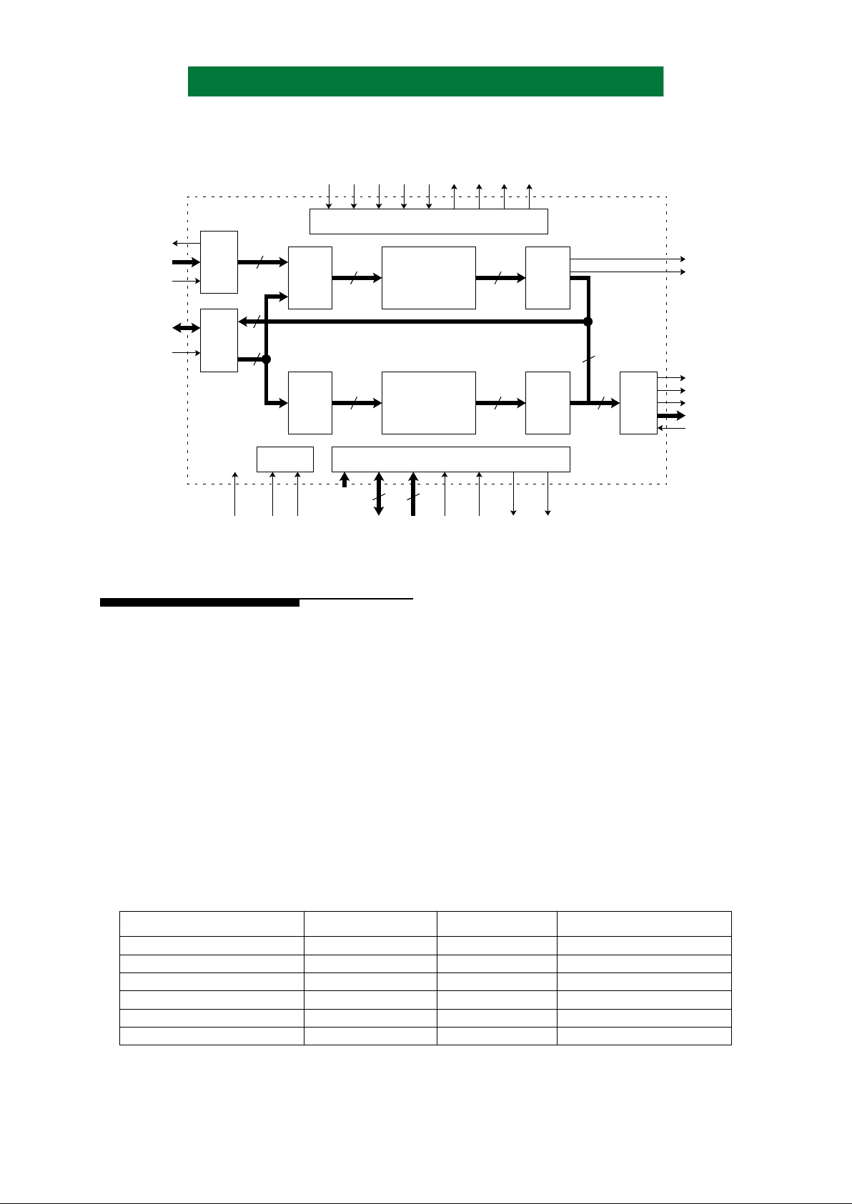
Figure 1: Functional Block Diagram
1.3 FUNCTIONAL OVERVIEW
The coprocessor device has t hree exter nal h igh
speed synchronous data ports capable of
transferring once ever y cloc k cycl e. Thes e are a 32bit bidirectional dat a port, an 8-bit V ideo Input Data
(VID) port and a Video Output Data (VOD) port.
The 32-bit port is capable of transferring up to 4
bytes per clock. The VID and VOD are capable of
up to one byte per clock.
The device accepts uncompressed data through
the 8-bit VID port or the 32-bit data port in to its
Compression In FIFO (CI FIFO). The 32-bit data
port may be configured for 16-bit transfers.
Compressed data is available through the 32-bit
data port via the Compressed Output FIFO (CO
FIFO). The sustained data rate through the
compression engine is one byte per clock.
Decompression data may be simultaneously
processed by the device. Decompression data is
accepted through the 32-bit data port, buffered in
the Decompression Input FIFO (DI FIFO) and
decompressed. The output da ta is made available on
the 32-bit data port via th e Decompression Output
FIFO (DO FIFO) or the 8-bit Video Output port.
The decompression en gine is cap able of process ing
an uncompressed byte every clock.
The four FIFOs are organized as 16×32 each.
For data transfers through the three ports, the
“effective” FI FO sizes differ according to the ir data
bus widths. The table below shows the size of the
data port and the “effective” FIFO size for the
various configurations supported by the device.
Table 1: Data Bus and FIFO Sizes Supported by AHA3431
(From Scanner)
VIREQN
VID[7:0]
VIACKN
D[31:0]
DRIVEN
TEST
CLK
RSTN
PROCMODE[1:0]
PD[7:0]
PA[5:0]
CSN
DIR
RDYN
INTRN
VOACKN
VOD[7:0]
VOREQN
VOEORN
VOEOTN
(To Printer)
COEORN
DOREQN
COREQN
DIREQN
CIREQN
SD
DOACKN
COACKN
DIACKN
CIACKN
VID
PORT
DATA
PORT
CI
FIFO
16x32
DI
FIFO
16x32
CLOCK
DATA PORT CONTROL
COMPRESSOR
DECOMPRESSOR
MICROPROCESSO R INT ERFACE
CO
FIFO
16x32
DO
FIFO
16x32
VOD
PORT
AHA3431
StarLite
TM
8
8 8
888
32
32 32
6
8
COEOTN
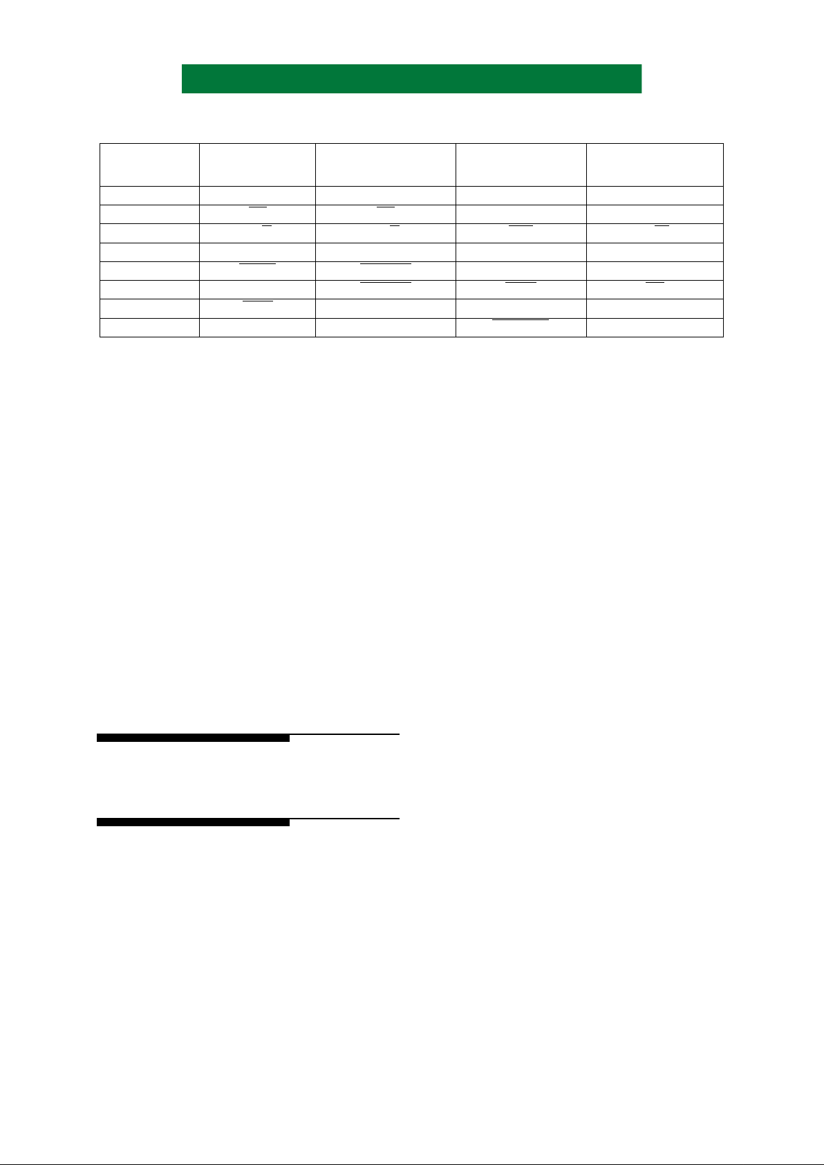
OPERATION DATA BUS WIDTH PORT EFFECTIVE FIFO SIZE
Compression Data In 8 Video In 16 x 8
Compression Data In/Out 32 Data Port 16 x 32
Compression Data In/Out 16 Data Port 16 x 16
Decompression Data In/Out 32 Data Port 16 x 32
Decompression Data In/Out 16 Data Port 16 x 16
Decompressed Data Out 8 Video Out 16 x 8
PS3431-0500 Page 3 of 50
Advanced Hardware Architectures, Inc.
Table 2: AHA3431 Connection to Host Microprocessors
Movement of data for compression or
decompression is performed using synchronous
DMA over the 32-bit data port. The Video ports
support synchronous DMA mode transfers. The
DMA strobe conditions are co nfigurabl e for the 32 bit data port depending upon the system processor
and the available DMA controller.
Data transfer for compres sion or
decompression is synchronous over the three data
ports functioning as DMA masters. To initiate a
transfer into or out of the Video ports, the device
asserts VxREQN, the external device responds with
VxACKN and begins to t ra nsf er da ta over the VID
or VOD busses on each succeeding rising edge of
the clock until VxREQN is deasserted. The 32-bit
port relies on the FIFO Threshold settings to
determine th e transfer.
The sections below describe the various
configurations, programming and other special
considerations in developing a compressi on system
using AHA3431.
2.0 SYSTEM CONFIGURATION
This section provides information on
connecting AHA3431 to various microprocessors.
2.1 MICROPROCESSOR INTERFACE
The device is capable of in te rf acing directly to
various processors for embedd ed applicatio n. T able
2 and Table 3 show how AHA3431 should be
connected to various host microprocessors.
All register accesses to AHA3431 are
performed on the 8-bit PD bus. The PD bus is the
lowest byte of the 32-bit microprocessor bus.
During reads of the internal registers, the upper 24
bits are not driven. System designers should
terminate these lines with Pullup resistors.
AHA3431 provides four modes of operation f or
the microprocessor p ort. Both active high and a ctive
low write enable si gnals are al lowed a s well as t wo
modes for chip select. T he mode of oper atio n is set
by the PROCMODE[1:0] pins. The
PROCMODE[1] signal selects when CSN must be
active and also how long an access lasts.
When PROCMODE[1] is high, CSN
determines the le ngth of the acces s. CSN must be at
least 5 clocks in length. On a read, valid data is
driven onto PD[7:0] during th e 5th clock. If CSN is
longer than 5 clocks, t hen valid data c ontinues to be
driven out onto PD[7:0]. When CSN goes inactive
(high), PD[7:0] goes tristate (asynchronously) and
RDYN is driven high async hronously . CSN must be
high for at least tw o clocks. RDYN is always drive n
(it is not tristate d when PR OC M OD E[ 1 ] is high) . The
mode is typical of processors such as the Motorola
68xxx.
When PROCMODE[1] is low, accesses are
fixed at 5 clocks, PD[7:0] is onl y driven dur ing the
fifth clock, and RDYN is driven high for the f irst 4
clocks and low during the fifth clock. RDYN is
tristated at all other times. Write data must be driven
the clock af ter CSN is sam pled low. Accesses may
be back to back with no delays in between. This
mode is typical of RISC p rocessors such as the i960.
PROCMODE[0] determines th e pol arit y of t he
DIR pin. If PROCMODE[0] is high, then the DIR
pin is an active low write en able. If PROCMODE[0]
is low, then the DIR pin is an active hig h write
enable. Figure 2 through Figure 5 illustrate the
detailed timing diagrams for the microprocessor
interface.
For additional notes on interfacing to various
microprocessors, refer to AHA Application Note
(ANDC16), Designer’ s Guide for StarLite
TM
Family
Products. AHA Applications Engineering is
available to supp ort with other pr ocessors not i n the
Designer’s Guide.
PIN NAME i960Cx i960Kx IDT3081
Motorola
MCFS102(ColdFIRE)
PA A LAD Latched Address Latched Address
CSN CS
CS System Dependent Decoded Chip Select
DIR W/R
W/R WR R/W
PD D LAD A/D A/D[7:0]
SD WAIT
READY System Dependent System Dependent
RDYN No Connect READY
ACK TA
DRIVEN DEN System Dependent System Dependent System Dependent
CLOCK PCLK No Connect SYSCLK
BCLOCK
Page 4 of 50 PS3431-0500
Advanced Hardware Architectures, Inc.
Table 3: Microprocessor Port Configuration
Figure 2: Microprocessor Port Write (PROCMODE[1:0]=“01”)
Figure 3: Microprocessor Port Read (PROCMODE[1:0]=“01”)
PROCMODE[1:0] DIR CYCLE LENGTH EXAMPLE PROCESSOR
00 Active high write fixed i960
01 Active low write fixed
10 Active high write variable
11 Active low write variable 68xxx, MIPS R3000
CLOCK
PA[5:0]
CSN
DIR
PD[7:0]
A0
RDYN
A1
D0 D1
CLOCK
PA[5:0]
CSN
DIR
PD[7:0]
A0
RDYN
A1
D0
A2
D1
PS3431-0500 Page 5 of 50
Advanced Hardware Architectures, Inc.
Figure 4: Microprocessor Port Write (PROCM ODE[1:0]=“11”)
Figure 5: Microprocessor Port Read (PROCMODE[1:0]=“11”)
CLOCK
PA[5:0]
CSN
DIR
PD[7:0]
A0
RDYN
A1
D0
CLOCK
PA[5:0]
CSN
DIR
PD[7:0]
A0
RDYN
A1
D0
Page 6 of 50 PS3431-0500
Advanced Hardware Architectures, Inc.
3.0 FUNCTIONAL DESCRIPTION
This section describes the various data ports,
special handling, data formats and clocking
structure.
3.1 DATA PORTS
AHA3431 contains two data input por ts, CI and
DI, and two data output ports, CO and DO on the
same 32-bit data bus, D[31:0]. Data transfers are
controlled by external DMA control. The logical
conditions under which data is written to the input
FIFOs or read from the output FIFOs are set by t he
DSC (Data Strobe Condition) field of the
System
Configuration 1 register.
A strobe condition defines under what logical
conditions the input FIFOs ar e written or the output
FIFOs read. CIACKN, COACKN, DIACKN,
DOACKN, and SD pins combine to strobe data in a
manner similar to DMA controllers. The DMA
Mode sub-section describe s the var ious da ta st robe
options.
3.2 DMA MODE
On the rising edge of CLOCK when the stro be
condition is met, the port with the active
acknowledge either strobes data into or out of the
chip. No more than one port may assert
acknowledge at any one time. Table 4 shows the
various conditions that may be programmed into
register DSC.
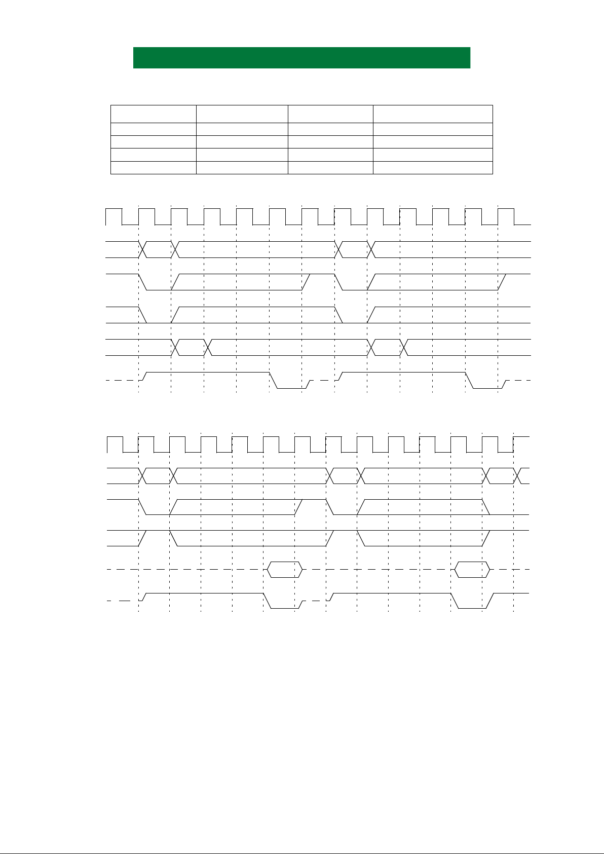
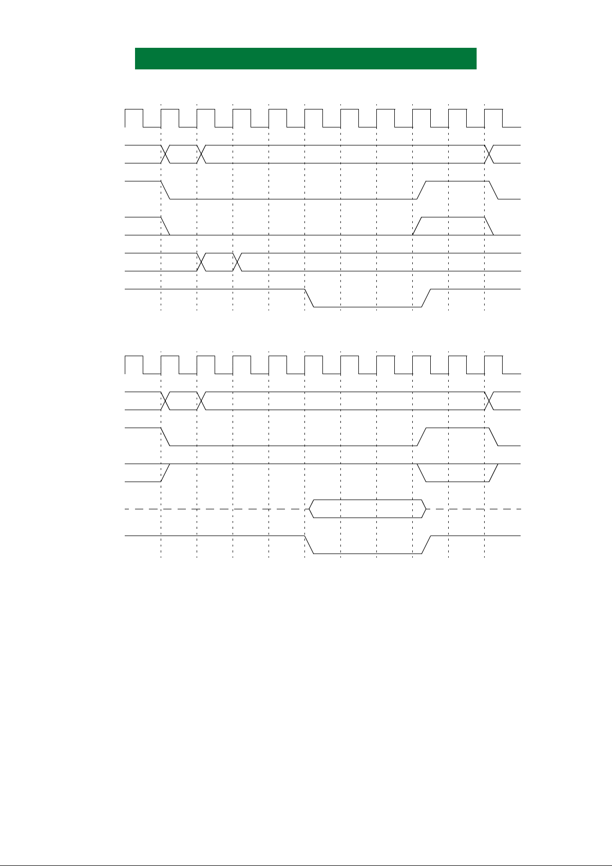
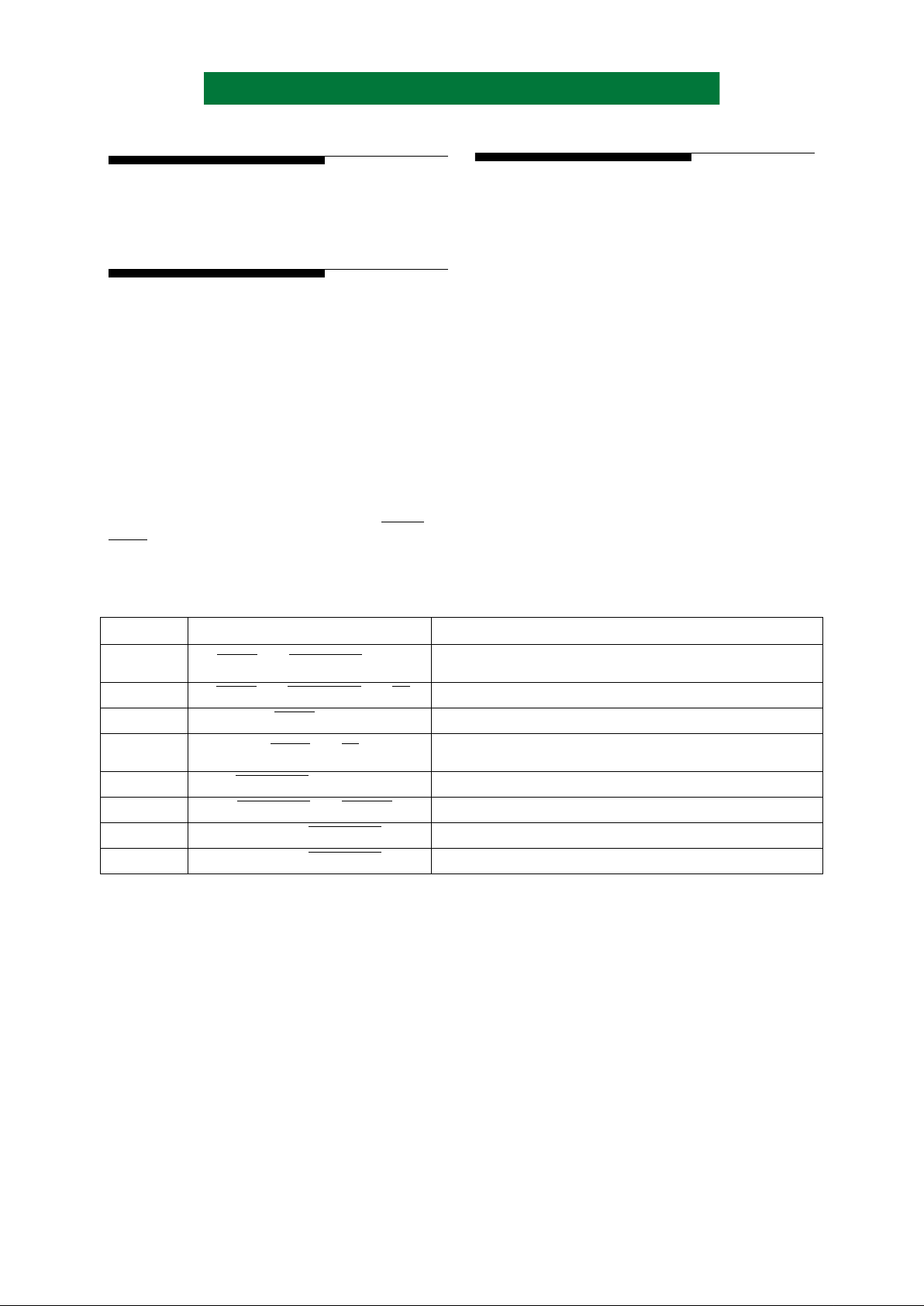
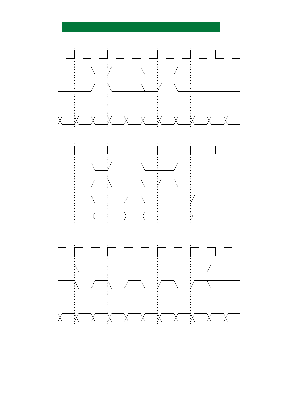
Figure 6 through Figure 11 illustrate the DMA
mode timings for single, four word and eight word
burst transfers for DSC=100 selection. For other
DSC settings, please refer to Appe ndix A. Note that
the only differe nce between odd and eve n values of
DSC is the polarity of SD. Waveforms are only
shown for polari ties of SD correspondi ng to specific
systems.
Table 4: Internal Strobe Conditions for DMA Mode
DSC[2:0] LOGIC EQUATION SYSTEM CONFIGURATION
000
i960Cx with inter nal DMA cont roller. SD is connecte d to
WAITN.
001 No specifi c system
010 General purpose DMA controller
011
i960Kx with external, bus master type DMA controller.
SD is connected to RDYN.
100 No specifi c system
101 No specifi c system
110 No specific system
111 No specific syst em
ACKN()& ACKN
delayed
()& SD)(
ACKN()& ACKN
delayed
()& SD()
ACKN()& SD()
ACKN()& SD()
ACKN
delayed
()& SD
delayed
()
ACKN
delayed
()& SD
delayed
()
ACKN()& ACKN
delayed
()
ACKN()& ACKN
delayed
()
ACKN
delayed
ACKN delayed 1 clock=
SD
delayed
SD delayed 1 clock=
PS3431-0500 Page 7 of 50
Advanced Hardware Architectures, Inc.
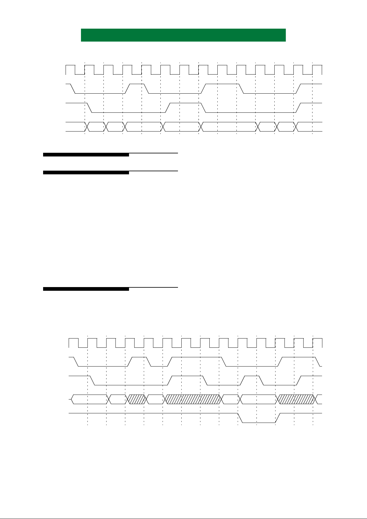
Figure 6: DMA Mode Timing for Single Word Writes, Strobe Condition of DSC=100
Figure 7: DMA Mode Timing for Single Word Reads, Strobe Condition of DSC=100
Figure 8: DMA Mode Timing for Four Word Burst Write, One Wait State, Strobe Condition
of DSC=100
CLOCK
ACKN
SD
DRIVEN
D
D0 D1
CLOCK
ACKN
SD
DRIVEN
D
D1D0
CLOCK
ACKN
SD
DRIVEN
D
D0 D2D1 D3
Page 8 of 50 PS3431-0500
Advanced Hardware Architectures, Inc.
Figure 9: DMA Mode Timing for Four Word Burst Read, One Wait State, Strobe Condition
of DSC=100
Figure 10: DMA Mode Timing for Eight Word Burst Write, Zero Wait State, Strobe Condition
of DSC=100
Figure 11: DMA Mode Timing for Eight Word Burst Read, Zero Wait State, Strobe Condition
of DSC=100
CLOCK
ACKN
SD
DRIVEN
D
D1D0 D2 D3
CLOCK
ACKN
SD
DRIVEN
D
D0 D2D1 D3 D4 D5 D6 D7
CLOCK
ACKN
SD
DRIVEN
D
D0 D2D1 D3 D4 D5 D6 D7

PS3431-0500 Page 9 of 50
Advanced Hardware Architectures, Inc.
3.3 PAD WORD HANDLING IN
BURST MODE
The StarLite compr ession algorit hm appends
a 15 bit End-of-Record codeword to terminate a
compression record. If a word containing an Endof-Record comes out during a bur st read, the words
following the End-of-Record are invalid (pad)
words. This prevents a burst read from crossing
record boundaries. The first word of the next burst
read is the first word of the next record. Any pad
words not previously removed must be deleted.
T wo methods are a vailable to de lete pad words.
During decompression pad words may be deleted
by using the Decompression Pause on Record
Boundaries bit (DPOR), in the Decompression
Control register. After the part is paused, the DI
FIFO must be reset by asserting the DIRST bit in the
Port Control register. Decompressor must also be
reset by ass erting DDR bi t in Decompression
Control register. The COEOTN signal is asserted
when an End-of-Record is present on the output of
the CO FIFO and the compression record counter
has decremented to z er o , t hus i ndi cat ing the end of
a transfer comprised of o ne or more com pressed
records.
Another method to remove pad words during
compression is to read the Compressed Byte Count
register after pausing at an End-of-Record and
subtract this from the system’s received word count.
This difference is the number of pad words that
must be removed from the end of the compressed
record.
The COEORN signal is asserted when an Endof-Record is present on the out put of the CO FIFO.
COEORN is deasserted after the transfer. In some
systems COEORN can be used to generate a DMAdone condition if conditioned with the
acknowledge.
3.4 DMA REQUEST SIGNALS
AND STATUS
AHA3431 requests data using request pins
(CIREQN, DIREQN, COREQN, DOREQN). The
requests are controlled by programmable FIFO
thresholds. Both input and output FIFOs have
programmable empty and full thresholds set in the
Input FIFO Thr eshold
and Outpu t FIFO Thr eshol d
registers. By requesting only when a FIFO can
sustain a ce rtain burst size, the bus is used more
efficiently.
Operation of these req uest signals should not be
confused with the request signals o n the video ports.
CIREQN or DIREQN active indicates space
available in the particular input FIFO, and
COREQN or DOREQN active indicates data is
available in the particular output FIFO. These
request signals inactive does not prevent data
transfers. The data trans fers are controlled solely
with the particular a cknowledge signal be ing active.
The input requests, CIREQN and DIREQN,
operate under the fol lowing priori tize d ru les, li sted
in order of highest to lowest:
1) If the FIFO reset in the
Port Control
register is active, the request is inactive.
2) If a FIFO overflow interrupt is active, the
request is inactive.
3) If the FIFO is at or below the empty
threshold, the request remai ns acti ve.
4) If the FIFO is at or above the full threshold,
the request s tays inactive.
The output requests, COREQN and DOREQN,
operate under the fol lowing priori tize d ru les, li sted
in order of highest to lowest:
1) If the FIFO reset in the
Port Control
register is active, the request is inactive.
2) If the output FIFO underflow interrupt is
active, the request is inactive.
3) If an EOR is present in the output FIFO, th e
request goes active.
4) If the output FIFO is at or above the full
threshold, the request goes acti v e.
5) If an EOR is read (strobed) out of the FI FO,
the request goes inactive during the same
clock as the strobe (if ERC=0), otherwi se it
goes inactive on the next clock.
6) If the output FIFO is at or below the empt y
threshold, the request goes inact iv e.
3.4.1 FIFO THRESHOLDS
For maximum efficiency, the FIFO thresholds
should be set in such a way that the compressor
seldom runs out of data from the CI FIFO or
completely fills the output FIFO. The FIFOs are 16
words deep.
For example, in a system with fixed 8-word
bursts, good values for the thresholds are:
IET=3, IFT=4, OFT=D, OET=C
Setting the input full threshold to one higher
than the input empty threshold simply guarantees
that the request deasserts as soon as possible. The
latency between a word being strobed in and the
request changing due t o a FIFO threshold condi tion
is 3 clocks. This should be kept in mind when
programming threshold value s. Refer to Section 4.0
of AHA Application Note (ANDC16), Designer’s
Guide for StarLite
TM
Family Products for a more
thorough discussion of FIFO thresholds. The
following figure shows an example of an input
FIFO crossing its full threshold.
Page 10 of 50 PS3431-0500
Advanced Hardware Architectures, Inc.
Figure 12: FIFO Threshold Example (IFT=4, DSC=2, 1 Word Already in FIFO)
Note: CIREQN deasserted when threshold counter exceeds IFT=4, but additional words are reading as long as
ACKN is asserted.
Figure 13: Request vs. End-of-Record, Strobe Condition of DSC=010
3.4.2 REQUEST DURING AN END-OF-RECORD
The request deasserts at an EOR in one of two
ways. If ERC bit in Sy stem Conf igurati on 1 is zero,
the request deasserts asynchronously during the
clock where the EOR is strobed out of the FIFO.
This leads to a lo ng output delay for REQN, but may
be necessary in some systems. For DSC values of 4
or 5, the request deasserts the first clock after the
acknowledge pulse for the EOR. If ERC is set to
one, then the request deasserts synchronously the
clock after the EOR is strobed out. The minimum
low time on the request in this case is one clock.
The request delay varies between the different
strobe conditions. See Section 8.0 AC Electrical
Specifications for further details.
3.4.3 REQUEST STATUS BITS
An external microproc essor can also read the
value of each reque st using the CIREQ and COREQ
bits in the Compression Port Status register and the
DIREQ and DOREQ bits in the Decompression
Port Status register. Please note the request status
bits are active high while the pins are active low.
CLOCK
D
CIACKN
CIREQN
Threshold
1
2
3
45
6
7
8
1
234
5
6
78
9
Counter
EOR-2
CLOCK
D
ACKN
REQN
EOR-1
EOR
(ERC=0)
EORN
REQN
(ERC=1)

PS3431-0500 Page 11 of 50
Advanced Hardware Architectures, Inc.
3.5 DATA FORMAT
The width of the D bus is selected with the
WIDE bit in System Configuration 0. If WIDE=1,
then D is a 32-bit bus. If WIDE=0, D is a 16-bit bus.
If the bus is configured to be 16-bits wide
(WIDE=0), all data tran sfe rs occur on D[15:0] and
the upper 16 bits of the bus, D[31:16], should be
terminated with Pullup res istors. If WIDE=0, the
FIFO is sixteen words deep.
Since the compression algorithm is byte
oriented, it is necessary for AHA3431 to know the
ordering of the bytes within the word. The COMP
and DECOMP BIG bits in System Configuration 0
select between big endian and little endian byte
ordering for the compression and decompression
channel. Little endian stores the first byte in the
lower eight bits of a word (D[7:0]). Big endian
stores the first byte in the uppermost ei ght b it s of a
word (D[31:24 ] for WI D E= 1 , D[ 1 5: 8 ] for WI DE = 0 )
for the decompression engine or compression
engine.
REVERSE BYTE in the System Configuration
0 register allows the bit order into the compression
engine to be swapped. This control is useful for
reversing a page of data for duplex printing
applications and has no significant impact on
compression ratio performanc e.
3.6 ODD BYTE HANDLING
All data transfers to or from either the
compression or decompression engines are
performed on the D bus on word b ounda ries . Since
no provision is made for single byte transfers,
occasionally words will contain pad bytes.
Following is a descriptio n of when t hese pad bytes
are necessary for each of the data interfaces.
3.6.1 COMPRESSION INPUT AND PAD BYTES
Uncompressed data input into AHA3431 is
treated as re cords. The le ngth of these r ecords is
fixed by the value in the Record Length or RLEN
register. This register contains the number of
uncompres sed bytes in each record. If th e value in
RLEN is not an integer multiple of n umber of bytes
per word as selec ted by WIDE, the fi nal word in the
transfer of the record contains pad bytes. The
compression engine simpl y discards these pad bytes
and has no effect on either the dictionary or the
output data stream. The next re cord must begin on a
word boundary.
The minimum value for RLEN is 4 bytes.
3.6.2 COMPRESSION OUTPUT AND
PAD BYTES
If a record ends on a byte other than the l ast byte
in a word, the final word contains 1, 2 or 3 pad bytes.
The pad bytes have a value of 0x00. Th is applies t o
the 32-bit data port only.
3.6.3 DECOMPRESSION INPUT, PAD BYTES
AND ERROR CHECKING
This port recognizes th e end of a re cor d by the
appearance of a special End-of- Record se quence in
the data stream. Once this is seen, the remaining
bytes in the current word are treated as pad bytes
and discarded. The word following the end of the
record is the beginning of the next record.
When operating in decompression mode, the
Decompression Record Length (DRLEN) register
can be used to provid e error checking. The e xpected
length of the decompressed record is programmed
into the DRLEN register. The decompressor then
counts down from the value in DRLEN to zero.
A DERR inter r upt is issued if an EOR is not
read out of the decompressor when the counter
expires or if an EOR occurs before the counter
expires (i.e., when the record length s do not match).
If the DERR interrupt is masked, us e of the DRLEN
register is optional.
When operating in pass-t hrough mode, there is
no End-of-Record codeword for the decompressor
to see. In pass-through mode, the user must set the
record length in the DRLEN register.
3.6.4 DECOMPRESSION OUTPUT AND
PAD BYTES
When the decompressor detects an End-ofRecord codeword, it will add enough pad bytes of
value 0x00 to complete the current word as defined
by the WIDE bit in the System Configuration 0
register. For example, if a record ends on a byte
other than the last byte in a word, the final word
contains 1, 2 or 3 pad bytes. This applies to the 32bit data port only, not the VOD port. The VOD port
never outputs pad bytes since it is 8-bits wide.
Page 12 of 50 PS3431-0500
Advanced Hardware Architectures, Inc.
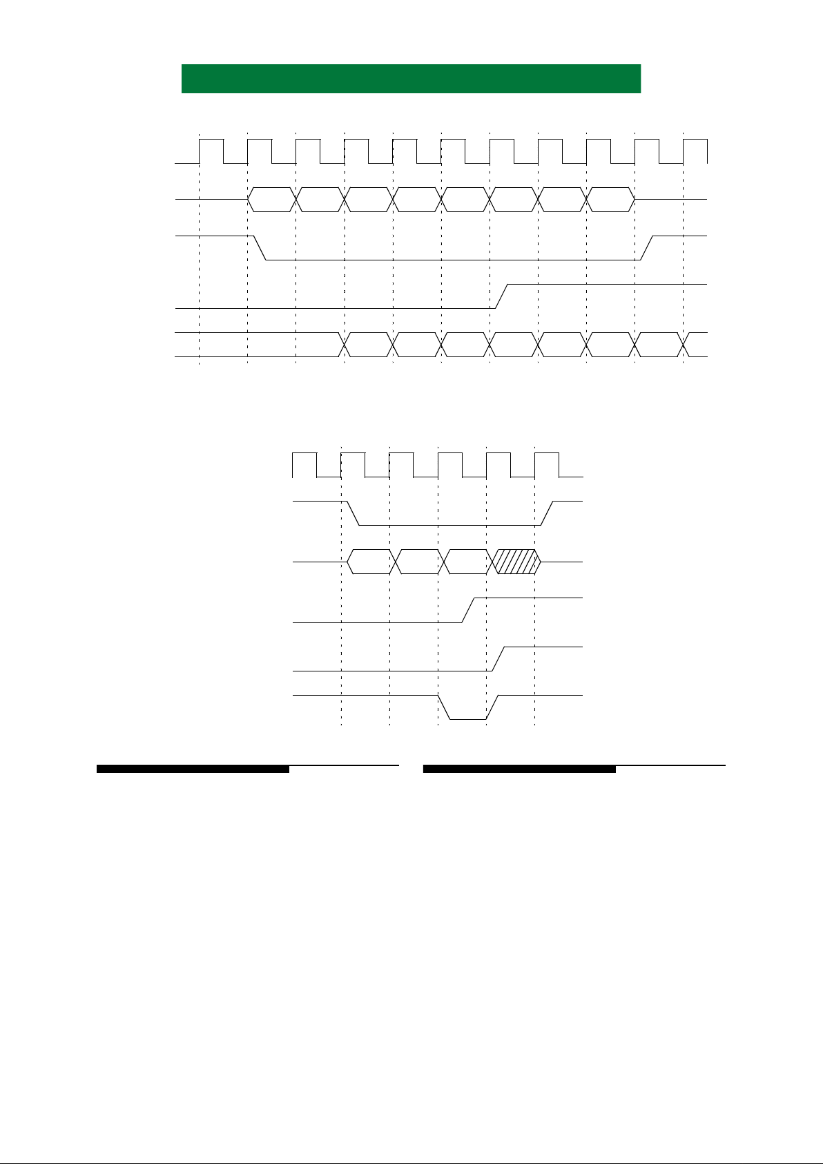
Figure 14: Timing Diagram, Video Input
3.7 VIDEO INTERFACES
3.7.1 VIDEO INPUT
The video input port is enabled by the VDIE bit
in the System Configuration 1 register . The port use s
VIREQN to indicate that the port can accept another
byte. The value on VID[7:0] is written into
AHA3431 each clock that VIREQN and VIACKN
are both low.
The video input port as serts VIREQN whenever
there is room in the CI FIFO. The value s in IET and
IFT are all ignored. Th e compressi on input FI FO is
16 bytes deep in this mode. The video input port can
transfer up to one byte per clock (33MB/sec). The
DMA interface cannot access t he compression input
FIFO when VDIE is set.
3.7.2 VIDEO OUTPUT
The video output port is enabled by the VDOE
bit in the System Configuration 1 regist er. The port
uses VOREQN to indicate that the byte on
VOD[7:0] is valid. An 8-bit word is read ea ch clock
when both VOREQN and VOACKN are sampled
low on a rising edge of CLOCK. Pad bytes at an end
of record are discarde d by the video output po rt and
do not appear on VOD[7:0]. When the byte on
VOD[7:0] is the last by te in a record, the VOEORN
signal goes low. To use VOEORN as an End-ofRecord indicator, it should be conditioned with
VOREQN and VOACKN. Unlike a DMA transfer,
there are no pad bytes after an End-of-Record.
VOEOTN operates similar to VOEORN. It
flags the end of an output transfer of one or more
decompressed records. VOEOTN is as ser te d when
the End-of-Record is at the out put of t he DO FIFO
and the decompression record count has
decremented to zero.
The port requests whenever a valid byte is
present on the output. The values in OET and OFT
are all ignored. The decompression output FIFO is
16 bytes deep in this mode. The video output port
can output up to one byte per clock. The DMA
interface cannot access the decompression output
FIFO when VDOE is set.
Figure 15: Timing Diagram, Video Output
CLOCK
VIREQN
VIACKN
VID[7:0]
0 3
don’t
care
1 2
don’t care
4 5
don’t
care
CLOCK
VOREQN
VOACKN
VOD[7:0]
0 31 2 4 5
VOEORN,
VOEOTN

PS3431-0500 Page 13 of 50
Advanced Hardware Architectures, Inc.
3.8 ALGORITHM
AHA3431 compression is an efficient
implementation of an algorithm optimized for
bitonal imag es. For some comparison data refer to
the AHA Application Note ( AN D C1 3 ),
Compression
Performance: StarLiteTM: ENCODEB2 on
Bitonal Images. A software emulation of the
algorithm is available for evaluation.
3.9 COMPRESSION ENGINE
The compression engine supports either
compression or pass-through processes. The
compression engine is enabled with the COMP bit in
the Compr ession Contr ol register. When the engine is
enabled, it takes data from the CI F I FO as it becomes
available. This data is either compressed by the engine
or passed through unaltered. This pass-through mode
is selected with the CPASS bit in the Compr ession
Control regi ster . The CPASS bit may on ly be changed
when COMP is set to ‘0’. The contents of the
dictionary are preserved when COMP is changed.
However, when CPASS is changed, the contents are
lost. Consequently, the device cannot be changed from
pass-through mode to compression mode or vice versa
without losing the contents of the dictionary.
The compressor can be instr uct ed to ha lt at t he
end of a record or an end of multip le-record transfer .
If the CPOR bit is set, the c ompressor stops taking
data out of the CI FIFO immediately after the last
byte of a record, and the COMP bit is cleared. If the
CPOT bit is set the compressor halts at the end of the
multiple-record transfer. The CEMP bit indicates
the compressor has em ptied all data. Compression is
restarted by setting the COMP bit.
The compression engine takes dat a fr om the
compression input FIFO at a maximu m rate of 33
MBytes/sec. Two conditions cause t he data rate to
drop below the maximum. The first is caused by the
compression input FIFO running empty of dat a to be
compressed. The second conditi on i s ca used b y the
output FIFO filling. Whe n thi s occ urs , the engi ne
halts and waits for the FIFO. While halt ed, the engine
goes into a low power standby mode. Refe r to the
table in Section 7.1 for the e xte nt of power savings.
The compression byte counter counts the number
of bytes output from the CO data port. The counter is
valid to read after a compression end of transfer
interrupt (CEOT), or pausing after End-of-Record.
3.10 DECOMPRESSION ENGINE
The decompression engine is enabled with the
DCOMP bit in the Deco mpr ession Contr ol register .
When the engine is enabled, it takes data from the
DI FIFO as it becom es avai lable. This dat a is eith er
decompressed by the engine or passed through
unaltered. Pass-through mode is selected with the
DPASS bit. DPASS may only be changed when
DCOMP is set to zero and DEMP is s et to one. Th e
contents of the dictionary are preserved when
DCOMP is changed. However, when DPASS is
changed, the contents are lost. Consequently,
AHA3431 cannot be changed from pass-through
mode to decompression mode or vice versa without
losing the contents of the dictionary.
The decompressor can be instructed to halt at
the end of a record or an end of multiple-record
transfer. If the DPOR bit is set, the decompressor
stops taking data out of the DI FIFO immediately
after the last byte of a recor d, and the DCOMP bit is
cleared. If DPOT bit is set the decompressor halts at
the end of the multiple-record transfer. The DEMP
bit indicates the decompressor has emptied of all
data. Decompression is restarted by setting the
DCOMP bit. If DPOR or DPOT is set and data from
a second record enters the FIFO immediately after
the first record, bytes from the second record will
have entered the decompre ssor prior to decoding the
EOR. An implication of this is that bytes from the
second record will r emain i n th e deco mpres sor an d
prevent DEMP from setting after all of the data from
the first record has left the d ecompressor. This
differs from ope ration of the compression e ngine. In
either mode, a DEOR interrupt is generated when
the last byte of a decompressed rec ord is read ou t of
the chip, and DEOT when the last byte of a transfer
is read out of the chip.
The decomp ressor takes data from the
decompression input FIFO at the maximum clock
rate. AHA3431 can maintain this data rate as long as
the decompression input FIFO is not empty or the
decompression output FIFO is not full.
Caveat: Changing the mode for the de compressor
between records or multiple-record t ransfers must be
done with the data of the following record or tr ansfer
held off until the DEOR status bit is t rue for the current
record and the Decompression Control registers have
been reprogrammed. This reprogramming can occur
automatically with pre arm ing.
3.11 PREARMING
Prearming is the ability to write certa in regist ers
that apply to the next record while the device is
processing the current record. Prearmi ng occurs
automatically at the end of a record. I f a prearmable
register is written while the part i s busy pro cessing a
record, at the end of the record the part takes its progr am
from the register value last written. Com pression
Control and Decompression Control registers each
have separate corresponding prearm registe rs.

Page 14 of 50 PS3431-0500
Advanced Hardware Architectures, Inc.
The lower 3 bytes of both the Compression
Record Length and the Decompression Length
registers are prear mable. They may be changed and
the new values loaded into th e respective counte r at
the next End-of-Record. If the most significant byte
is written in either of the Record Length registers,
the counter is immediate ly reloaded wit h the new 4
byte value in the particular register.
3.12 INTERRUPTS
Nine conditions are reported in the Interrupt
Status/C ont rol 1 and Status/Control 2 registers as
individual bits. All interrupts are maskable by
setting the corres ponding bits in the Inter rupt Mas k
register . A one in the Interrupt Mask register means
the corresponding bit in th e Interrupt Status /Control
register is masked and does not affect the interrupt
pin (INTRN). The INTRN pin is active whenever
any unmasked interrupt bit is set to a one.
An End-of-Record interrupt is posted when a
word containing an end-of-record is strobed out of
the compression or decompression output FIFO
(CEOR and DEOR respectively). A DEOR
interrupt is also re ported if an end-of -record i s read
from the video output port. A compression or
decompression end of trans fer interrupt will also be
posted if this is the last record of a transfer.
End-of-Transfer interrupts are posted when an
EOR occurs that c auses the c ounter to decrement to
zero. These are CEOT and DEOT, and they apply to
both the compression and decompression engines
respectively.
Four FIFO error conditions are also reported.
Overflowing the input FIFOs generates a CIOF or
DIOF interrupt. An ove rflow can only be cleared by
resetting the respective FIF O via the Port Control
register.
Underflowing the output FIFOs (readi ng when
they are not ready) generates a COUF or DOUF.
Underflow interru pts are cleared by wri ting a one to
COUF or DOUF. In the event of an underflow, the
respective FIFO mus t be reset. Note that in systems
using fixed length b ursts which rearbit rate duri ng a
burst, the CO FIFO may request a nother burst when
the record actually finishes near the end of the
current burst. In this scenario a second burst takes
place causing a FIFO under flow . As long as a pause
on End-of-Record is used, d ata is not corrupted. The
FIFO simply must be reset.
3.13 DUPLEX PRINTING
Duplex Printing is the ability to print on both
sides of the page. AHA3431 supports this with
separate endian control for the Compressor and
Decompressor, and bit order control at the input to
the compressor . Bit order control allows revers al of
the data bits within each byte of data. For example,
reverse order means bi t-7 is swapped with bi t-0, bit-
6 is swapped with bit-1, etc.... Duri ng compres sion
operation of th e back side of the p age the data words
are sent to the AHA3431 device in reverse order.
The byte order is swapped if necessary by the
COMP BIG bit in the System Configuration 0
Register . The bit or der wit hin eac h byte i s reve rsed
with the REVERSE BYTE bit in this same register.
During decompression of th is reversed page the
DECOMP BIG bit in this register must be
programmed to the same value used when this p age
of data was compressed. Use of this feature has
virtually no effect on the compression ratio when
compared to compressing in forward order.
3.14 BLANK BANDS
Setting DBLANK in the Decompression
Control register ca uses the nex t record outpu t from
the Decompressor to be comprised of a repeating 8bit pattern defined by the Pattern register.
DBLANK automatically clears at the end of the
next record. This command bit may be prearmed by
writing to the Decompression Control Prearm
register . When progr amming the device to generate
blank records the system must not send data to be
decompressed until the device has reached the end
of record for the blank record.
3.15 LOW POWER MODE
The AHA3431 is a data-driven system. When
no data transfers are tak ing place, only the clock and
on-chip RAMs including the FIFOs re quire power.
To reduce power consumption to its absolute
minimum, the user can stop the clock when it is
high. With the system clock stopped and at a high
level, the current consumption is due to leakage.
Control and Status registers are preserved in this
mode. Reinitialization of Control registers are not
necessary when switching from Low Power to
Normal operating mode.
3.16 TEST MODE
In order to facilitate board level testing, the
AHA3431 provides the abili ty to tristate all output s.
When the TEST0 pin is high, all out puts of the chi p
are tristated. When TEST0 is low, th e chip returns to
normal operation.

PS3431-0500 Page 15 of 50
Advanced Hardware Architectures, Inc.
4.0 REGISTER DESCRIPTIONS
The microprocessor configures, controls and monitors IC operation through the use of the registers
defined in this section . The bits la beled “
res” are reserved and must b e set to zero when writ ing t o re giste rs
unless otherwise noted.
A summary of registers is listed below.
Table 5: Internal Registers
ADDRESS R/W DESCRIPTION FUNCTION
DEFAULT
AFTER
RSTN
PREARM
0x00 R/W System Configuration 0
Big Endian vs. Little Endian,
32-bit vs. 16-bit, Reve rse Byte
Undefined No
0x01 R/W System Configuration 1
Data Strobe Condition, EOR
Request Control, VDO Port
Enable, VDI Port Enable
0x00 No
0x02 R/W Input FIFO Thresholds
Input FIFOs Empty
Threshold, Full Threshold
Undefined No
0x03 R/W Output FIFO Thresholds
Output FIFOs Empty
Threshold, Full Threshold
Undefined No
0x04 R Compression Ports Status
FIFO Status, Request Status,
EOR Status
Undefined No
0x05 R Decompression Ports Status
FIFO Status, Request Status,
EOR Status
Undefined No
0x06 R/W Port Control Reset Individual FIFOs 0x0F No
0x07 R/W Interrupt Status/Control 1 EOR, Overflow, Underflow 0x00 No
0x09 R/W Interrupt Mask 1 Interrupt Mask bits 0xFF No
0x0A R Version Die Version Number 0x31 No
0x0C R/W
Decompre ssion Record
Length 0
Bytes Remaining, Byte 0 0xFF Yes
0x0D R/W
Decompre ssion Record
Length 1
Bytes Remaining, Byte 1 0xFF Yes
0x0E R/W
Decompre ssion Record
Length 2
Bytes Remaining, Byte 2 0xFF Yes
0x0F R/W
Decompre ssion Record
Length 3
Bytes Remaining, Byte 3 0xFF No
0x10 R/W Compression Record Length 0
Length of Uncompressed Data
in Bytes, Byte 0
Undefined Yes
0x11 R/W Compression Record Length 1 " " , Byte 1 Undefined Yes
0x12 R/W Compression Record Length 2 " " , Byte 2 Undefined Yes
0x13 R/W Compression Record Length 3 " " , Byte 3 Undefined No
0x14 R/W Compression Control
Pause on Record Boundaries,
Enable Com pression,
Compression Engine Empty
Status, Compressi on
Dictionary Reset, Select P assThrough Mode
0x04 Yes
0x15 R/W Compression Reserved Reserved 0x00 No
0x16 R/W Compression Line Length 0
Line Length Register Lower
8bits
Undefined No
0x17 R/W Compression Line Length 1
Line Length Register Upper
3bits
Undefined No

Page 16 of 50 PS3431-0500
Advanced Hardware Architectures, Inc.
0x18 R/W Decompression Control
Pause on Record Boundaries,
Enable Decompression
Engine, Decompression
Engine Empty Status,
Dictionary Reset, Enable
Pass-Through Mode
0x04 Yes
0x1A R/W Decompression Reserved 1 Reserved 0x00 No
0x1C R/W Decompression Line Length 0
Line Length Register Lower
8bits
Undefined No
0x1D R/W Decompression Line Length 1
Line Length Register Upper
3bits
Undefined No
0x20 R/W Compression Record Count 0
Compressor number of
records in a transfer
0xFF No
0x21 R/W Compression Record Count 1
Compressor number of
records in a transfer
0xFF No
0x27 R/W Interrupt Status/Control 2
Compression EOT Interrupt ,
Decompression EOT Interru pt
0x00 No
0x29 R/W Interrupt Mask 2
Interrupt Mask bits for CEOT,
DEOT
0xFF No
0x2C R/W Decompression Record Count 0
Decompressor number of
records in a transfer
0xFF No
0x2D R/W Decompression Record Count 1
Decompressor number of
records in a transfer
0xFF No
0x30 R Compression Byte Count 0
Compressed byte count,
byte 0
0x00 No
0x31 R Compression Byte Count 1
Compressed byte count,
byte 1
0x00 No
0x32 R Compression Byte Count 2
Compressed byte count,
byte 2
0x00 No
0x33 R Compression Byte Count 3
Compressed byte count,
byte 3
0x00 No
0x34 R/W Compression Control Prearm
Prearm Re gister for
Compression Control
0x00 No
0x35 R/W Pattern
8-bit pattern for blank record
generation
Undefined No
0x38 R/W Decompression Control Prearm
Prearm Re gister for
Decompression Control
0x00 No
0x3A R/W Decompression Reserved 2 Reserved 0x00 No
0x3F Reserved Reserved 0x0F No
ADDRESS R/W DESCRIPTION FUNCTION
DEFAULT
AFTER
RSTN
PREARM

PS3431-0500 Page 17 of 50
Advanced Hardware Architectures, Inc.
4.1 SYSTEM CONFIGURATION 0, ADDRESS 0x00 - READ/WRITE
After reset, its cont ents are undefined . It must be written be fore any input or out put data movement may
be performed.
COMP BIG-Selects between little or big endian byte order for the compressor. See table.
DECOMP BIG-Selects between little or big endian byte order for the decompressor. See table.
REVERSE BYTE- When this bit is one th e byte data entering the compressor is rever sed . Bit 0 i s s w appe d
with bit7, bit1 is swapped with bit6, bit2 is swapped with bit5, etc. . .
res - Bits must alway s be written wi th zeros.
WIDE - Selects between 32 and 16-bit D buses.
4.2 SYSTEM CONFIGURATION 1, ADDRESS 0x01 - READ/WRITE
This register is cleared by reset.
DSC[2:0] - Data S tr obe Cond it ion. Control the condition used to str obe da ta into and out of the data ports
on the D bus. T a ble 4 shows the p rogramming for t he strobe cond ition for va rious DMA modes.
res - Bits must alway s be written wi th zeros.
ERC - EOR Request Control. Determines when COREQN and DOREQN deassert at an End-of-
Record. If ERC=0, then the req uest deasser ts asynchronou sly during the clock when an EOR is
strobed out. If ERC=1, then the request deasserts synchronously the clock after an EOR is
strobed out. See Figure 18 through Figure 21.
Address
bit7 bit6 bit5 bit4 bit3 bit2 bit1 bit0
0x00 res WIDE res
REVERSE
BYTE
DECOMP
BIG
COMP
BIG
COMP BIG or
DECOMP BIG
WIDE DESCRIPTION
00
Little Endian data order 16-bit words
D[15:8] D[7:0]
Byte 1 Byte 0
01
Little Endian data order 32-bit words
D[31:24] D[23:16] D[15:8] D[7:0]
Byte 3 Byte 2 Byte 1 Byte 0
10
Big Endian data order 16-bit words
D[15:8] D[7:0]
Byte 0 Byte 1
11
Big Endian data order 32-bit words
D[31:24] D[23:16] D[15:8] D[7:0]
Byte 0 Byte 1 Byte 2 Byte 3
Address
bit7 bit6 bit5 bit4 bit3 bit2 bit1 bit0
0x01 res VDIE VDOE ERC res DSC[2:0]

Page 18 of 50 PS3431-0500
Advanced Hardware Architectures, Inc.
VDOE - VDO Port Enable. When this bit is set, the data from the decompression output FIFO goes to
the VDO port. When the bit is clear, the decompressed data is read by DMA on the D bus.
VDIE - VDI Port Enable. When this bit is set, the VDI port handshakes data and writes it into the
compression input FIFO. When the bit is clea r , the compressi on input FIFO is wri tten by DMA
from the D bus.
4.3 INPUT FIFO THRESHOLDS, ADDRESS 0x02 - READ/WRITE
After reset, its cont ents are undefined . It must be written be fore any input or out put data movement may
be performed.
IET[3:0] - Empty threshold for input FIFOs. If the number of words in the input FIFO (CI or DI) is less
than or equal to this numb er, the re quest for that channel is as serted.
IFT[3:0] - Full threshold for input FIFOs. If the number of words in the input FIFO (CI or DI) is greater
than or equal to this number, the request for the channel is deasserted.
4.4 OUTPUT FIFO THRESHOLDS, ADDRESS 0x03 - READ/WRITE
After reset, its cont ents are undefined . It must be written be fore any input or out put data movement may
be performed.
OET[3:0] - Empty threshold for output FIFOs. If the num ber of words in the output F IFO (CO or DO) is
less than or equal to this number , the reques t for the channel is deasserted (e xcept in the ca se of
an End-of-Record).
OFT[3:0] - Full threshold for output FIFOs. If the number of words in the output FIFO (CO or DO) is
greater tha n or equal to this number, the request for that channel is assert ed.
4.5 COMPRESSION PORTS STATUS, ADDRESS 0x04 - READ ONLY
This is a read only register. Writing to this register has no ef fect . After re set, its content s are undef ined.
CIFT - Compression input FIFO full threshold. This sig nal is act ive when the CI FIFO is greater than
or equal to the programmed FIFO full threshold. After reset and the Input FIFO Threshold
register has been written, this bit contains a zero.
CIREQ - Compression input request signal state. Reports the current state for the CIREQN pin. Notice
that this bit is active high while the pin is active low. Therefore, the value of this bit is always
the inverse of the value of the signal. After reset this bit contains a zero.
COET - Compression output FIFO empty th reshold. This bit is acti ve when the CO FIFO is les s than or
equal to the programmed FIFO empty threshold. After reset and the Output FIFO Threshold
register has been written, this bit contains a one.
COREQ - Compression output requ est signal state. Repor ts the current stat e for the COREQN pin. Notice
that this bit is active high while the pin is active low. Therefore, the value of this bit is always
the inverse of the value of the signal. After reset this bit contains a zero.
Address
bit7 bit6 bit5 bit4 bit3 bit2 bit1 bit0
0x02 IFT[3:0] IET[3:0]
Address
bit7 bit6 bit5 bit4 bit3 bit2 bit1 bit0
0x03 OFT[3:0] OET[3:0]
Address
bit7 bit6 bit5 bit4 bit3 bit2 bit1 bit0
0x04 COEMP CIEMP res CEOR COREQ COET CIREQ CIFT

PS3431-0500 Page 19 of 50
Advanced Hardware Architectures, Inc.
CEOR - Compression output end of rec ord. This bi t is act ive when the output FIF O contains t he end-of -
record code. After reset this bit contains a zero.
res - Bits must always be written with zeros.
CIEMP - Compression input empty. This bit is active when the CI FIFO is empty. After reset this bit
contains a one.
COEMP - Compression output empty. This bit is active when the CO FIFO is empty. After reset this bit
contains a one.
4.6 DECOMPRESSION PORTS STATUS, ADDRESS 0x05 - READ ONLY
This is a read only register. Writing to this register has no ef fect . After re set, its content s are undef ined.
DIFT - Decompression input FIFO full threshold. This signal i s active whe n the DI FI FO is at or a bove
the programmed FIFO full threshold. After reset and the Input FIFO Threshold register has
been written, this bit contains a zero.
DIREQ - Decompression input request signal state. Reports the current st ate for the DIREQN pin. Notice
that this bit is active high while the pin is active low. Therefore, the value of this bit is always
the inverse of the value of the signal. After reset this bit contains a zero.
DOET - Decompression output FIFO empty threshold. This bit is active when the DO FIFO is at or
below the programmed FIFO empty threshold. After reset and the Output FIFO Threshold
register has been written, this bit contains a one.
DOREQ - Decompression output request signal state. Reports the current state for the DOREQN pin.
Notice that this bit is active high while the pin is active low. Therefore, the value of this bit is
always the inverse of the value of the signal. After reset this bit contains a zero.
DEOR - Decompression output end of record. Thi s bit is act ive when the out put FIFO contains the End-
of-Record code. After reset this bit contains a zero.
res - Bits must always be written with zeros.
DIEMP - Decompression input empty. This bit is active when the DI FIFO is empty. After reset this bit
contains a one.
DOEMP - Decompression output empty . This bit is active when the DO FIFO is empty . After rese t this bit
contains a one.
Address
bit7 bit6 bit5 bit4 bit3 bit2 bit1 bit0
0x05 DOEMP DIEMP res DEOR DOREQ DOET DIREQ DIFT

Page 20 of 50 PS3431-0500
Advanced Hardware Architectures, Inc.
4.7 PORT CONTROL, ADDRESS 0x06 - READ/WRITE
This register is initialized to 0x0F after reset.
CIRST - Compression input reset. Setting this bit to a one resets the CI FIFO and clears state machines
on the compression input port. The reset condition remains active until the microprocessor
writes a zero to this bit.
CORST - Compression output reset. Setting this bit to a one resets the CO FIFO and clears state machines
on the compression output port. The reset condition remains active until the microprocessor
writes a zero to this bit.
DIRST - Decompression input reset. Setting this bit to a one resets the DI FIFO and clears the state
machines in the decompression input port. The reset condition remains active until the
microprocessor writes a zero to this bit.
DORST - Decompression output reset. Setting this bit to a one resets the DO FIFO and clears the state
machines in the decompression output port. The reset condition remains active until the
microprocessor writes a zero to this bit.
res - Bits must always be written with zeros.
4.8 INTERRUPT STATUS/CONTROL 1, ADDRESS 0x07 - READ/WRITE
This register is initialized to 0x00 after reset.
CEOR- Compression End-of-Record interrupt. This bit is set when an End-of-Record codeword is
strobed out of the compression output port. The microprocessor must write a one to this bit to
clear this interrupt.
DEOR - Decompression End-of-Record interrupt. This bi t is set when the last byte of a re cord is strobed
out of the decompression DMA or video output port. The microprocessor must write a one to
this bit to clear this interrupt.
DERR - Decompression Error. This bit is set if an EOR leaves the decompressor before DRLEN has
counted down to zero or if DRLEN counts to zero and the last byte is not an EOR. DERR is
only active in decompression mode (DPASS=0). The microprocessor must write a one to this
bit to clear this interrupt.
res - Bits must always be written with zeros.
CIOF - Compr ession Input FIFO Overflow. This interrupt is generated when a write to a n already full
CI FIFO is performed. Data written in this condit io n is los t. The only means of recovery from
this error is to reset the FIF O with the CIRS T bit. Resetting the FIFO causes this interru pt to
clear. CIREQN is inactive while the interrupt is set.
DIOF - Decompression Input FIFO Overflow. This interrupt is generated when a write to an already
full DI FIFO is performed. Data written in this condition is lost. The only means of recovery
from this error is to reset the FIFO with the DIRST bit. Resetting the FIFO causes this interrupt
to clear. DIREQN is inactive while the interrupt is set.
Address
bit7 bit6 bit5 bit4 bit3 bit2 bit1 bit0
0x06 res DORST DIRST CORST CIRST
Address
bit7 bit6 bit5 bit4 bit3 bit2 bit1 bit0
0x07 DOUF COUF DIOF CIOF res DERR DEOR CEOR

PS3431-0500 Page 21 of 50
Advanced Hardware Architectures, Inc.
COUF - Compression Output FIFO underflow. This interrupt is generated when a read from an empty
CO FIFO is performed. Once this interrupt is set, the CO FIFO must be reset with the CORST
bit. The microproce ssor must wr ite a one to this bit to cl ear this interr upt. COREQN is in active
while the interrupt is set.
DOUF - Decompression Output FIFO underflow. This interrupt is generate d when a read from an empty
DO FIFO is performed. Once this interrupt is set, the DO FIFO must be reset with the DORST
bit. The micropro cessor must write a one to this bi t to c lear this inte rrupt. DOREQN is i nactive
while the interrupt is set.
4.9 INTERRUPT MASK 1, ADDRESS 0x09 - READ/WRITE
This register is initialized to 0xFF after reset.
CEORM - Compression End-of-Recor d Interrupt Mas k. When set to a one, prevent s Compression End-of-
Record from causing INTRN to go active.
DEORM - Decompression End-of-Record Interrupt Mask. When set to a one, prevents Decompression
End-of-Record from causing INTRN to go active.
DERRM - Decompression Error Mask. When set to a one, prevents a decompre ssi on er ro r (DERR) fro m
causing INTRN to go active.
res - Bits must always be written with zeros.
CIOFM - Compression Input FIFO Overflow Mask. When set to a one, prevents a compression input
FIFO overflow (CIOF) from causing INTRN to go active.
DIOFM - Decompression Input FIFO Overflow Mask. When set to a one, prevents a decompression
input FIFO overflow (DIOF) from causing INTRN to go active.
COUFM - Compression Output FIFO Underflow Mask. When set to a one, prevents a compress ion output
FIFO underflow (COUF) from causing INTRN to go active.
DOUFM - Decompression Output FIFO Underflow Mask. When set to a one, prevents a decompression
output FIFO underflow (DOUF) from causing INTRN to go active.
4.10 VERSION, ADDRESS 0x0A - READ ONLY
VERSION[7:0] - Contains version number of the die. The AHA3431 returns the version number 0x31.
Address
bit7 bit6 bit5 bit4 bit3 bit2 bit1 bit0
0x09 DOUFM COUFM DIOFM CIOFM res DERRM DEORM CEORM
Address
bit7 bit6 bit5 bit4 bit3 bit2 bit1 bit0
0x0A VERSION[7:0]

Page 22 of 50 PS3431-0500
Advanced Hardware Architectures, Inc.
4.11 DECOMPRESSION RECORD LENGTH, ADDRESS 0x0C, 0x0D, 0x0E, 0x0F -
READ/WRITE
These registers are initialized to 0xFF after reset.
DRLEN[31:0]-Decompression Record Length. Contains the number of bytes in a decompressed record.
These registers provide different functions depending on whether the decompressor is in pass-
through or decompression mode. In decompress mode, the data itself contains EOR
information and DRLEN is only used for error checking. DRLEN is decremented each time a
byte leaves the decompressor.
In decompression mode, a DERR interrupt is issued if an EOR is not read out of the
decompressor when the counter expires or if an EOR occurs before the counter expires (i.e.,
when the record lengths do not match). If the DERR interrupt is masked, use of the DRLEN
register is optional in decompression mode.
In pass-through mode, DRLEN determines the size of records read out of the decompressor.
The counter is decremented for each byte read into the decompressor.
In either mode, the counter reloads when it reaches zero or when DRLEN[31:24] is written.
Reading DRLEN returns the number of bytes left in the count. The lower three bytes of this
register may be prearmed since the counter is automatically reloaded at the end of a record
when the part is not progra mmed to pause on End-of-Re cord. The upper byte i s not prearmable
since writing to this byte triggers an immediate reload to the counter.
4.12 COMPRESSION RECORD LENGTH, ADDRESS 0x10, 0x11, 0x12, 0x13 - READ/
WRITE
These registers are undefined after reset.
RLEN[31:0]-Record Length. Length of an uncompressed record in bytes. Writing these addresses sets a
register containi ng the l ength of a reco rd. Readi ng thes e addre sses re tu rns a co unter i ndica ting
the number of bytes remaining in the current record. The counter is decremented each time a
byte leaves the CI FIFO. The counter automatically reloads from the register at the end of a
record. The counter is also reloaded when RLEN[31:24] is written. The record length register
is also valid during pass-through operation. The lower three bytes of this register may be
prearmed since the counte r is automat ically r eloaded at the end of a re cord when the pa rt is not
programmed to pause on End-of -Record. The upp er byte is not prearmable si nce writing to t his
byte triggers an immediate reload to the counter.
The minimum value for RLEN is 4.
Address
bit7 bit6 bit5 bit4 bit3 bit2 bit1 bit0
0x0C DRLEN[7:0]
0x0D DRLEN[15:8]
0x0E DRLEN[23:16]
0x0F DRLEN[31:24]
Address
bit7 bit6 bit5 bit4 bit3 bit2 bit1 bit0
0x10 RLEN[7:0]
0x11 RLEN[15:8]
0x12 RLEN[23:16]
0x13 RLEN[31:24]

PS3431-0500 Page 23 of 50
Advanced Hardware Architectures, Inc.
4.13 COMPRESSION CONTROL, ADDRESS 0x14 - READ/WRITE
This register is initialized to 0x04 after reset.
CPOR - Compression Pause on record boundaries. When this bit is set to one, the compressor stops
taking data from the input FIFO once a record boundary is found. A record boundary is
indicated by the RLEN register decrementing to zero. Upon finding the record boundary,
COMP is cleared. This bit may only be changed when COMP is set to zero. After system reset,
this bit is cleared.
COMP - Compression. Setting this bit to a one enables the data compression engine (or pass-through
mode if CPASS is set) to take data from the compression input FIFO. If this bit is cleared,
compression stops. The bit is automatically clea red at the end of a record if CPOR is set or at
the end of a transfer if CPOT is set. The compression can be restarted without loss of data by
setting COMP. After reset, this bit is cleared.
CEMP - Compression engine empty. This bit is set to a one when no data is present inside the
compressor. Writing to this bit has no effect. After system re set, this bit is set.
CDR - Compression Dicti onary Reset. Setti ng this bit immediate ly resets the compr essor including th e
compression dictionary. The reset condition remains active until the microprocessor writes a
zero to this bit.
CPASS - Compression pass-through mode. While this bit is set, data is passed directly through the
compression engine without any effect on either the dictionary or the data itself. This bit may
only be changed when compression is disabled (COMP=0) and the compression engine is
empty of data (CEMP=0). The p ass -t hrough operation is st ar te d by setting COMP. To s top the
pass-through operat ion, COMP should be cleared (t o pause opera tion) and then CPASS may be
cleared.
CPOT - Compression Pause on Transfer boundaries. When this bit is set the compressor stops taking
data from the input FIFO once the end of transfer is reached indicated by the Record Counter
decrementing to zero. Upon finding the End of Tr ansfer boundary the COMP bit is cleared.
CPOT can only be set when COMP is cleared.
res - Bits must always be written with zeros.
CPREARM -Prearm Enable. When this bit is set, Compression Control Pr earm register is loaded into the
Compression Control register when the next end of record leaves the compressor.
4.14 COMPRESSION RESERVED, ADDRESS 0x15 - READ/WRITE
This register is used for production testing. Must be written with zero if at all. Resets to zero.
res - Bits must always be written with zeros.
Address
bit7 bit6 bit5 bit4 bit3 bit2 bit1 bit0
0x14 CPREARM res CPOT CPASS CDR CEMP COMP CPOR
Address
bit7 bit6 bit5 bit4 bit3 bit2 bit1 bit0
0x15 res

Page 24 of 50 PS3431-0500
Advanced Hardware Architectures, Inc.
4.15 COMPRESSION LINE LENGTH, ADDRESS 0x16, 0x17 - READ/WRITE
This register contains information necessary for the compression operation. It must be set prior to any
compression operatio n. It shou ld only be changed whe n COMP is cleare d and CEMP is set. Afte r changin g
compression line length, t he compressor should be reset using CDR. These regi sters are undefined after reset .
res - Bits must always be written with zeros.
LINE[10:0]-Line length. The number of bytes in the scan line is programmed here. Minimum value is 16.
4.16 DECOMPRESSION CONTROL, ADDRESS 0x18 - READ/WRITE
This register is initialized to 0x04 after reset. This register can be prearmed.
DPOR - Decompression Pause on reco rd boundaries. When this bit is set to on e, the decompressor stops
taking data from the input FIFO once a record boundary is found. Upon finding the record
boundary , DCOMP is cleared. This bit may only be changed wh en DCOMP is set to zero. After
system reset or DDR, this bit is cleared.
DCOMP - Decompression. Setting this bit to a one enables the decompression engine (or pass-through
mode if DPASS is set) to take data from the decompression input FIFO. If this bit is cleared,
decompression stops. The bit is automatically cleared at the end of a record if DPOR is set.
Decompression can be rest arted without loss of d ata by s et ti ng DCOMP. After system rese t or
DDR, this bit is cleared.
DEMP - Decompression engi ne empty. This bit is set when the decompression engine is cl eared of data.
Writing to this bit has no effect. After system reset, this bit is set.
DDR - Decompression Dictionary Reset. Setting this bit immediately resets the decompressor
including the decompression dictionary. The reset condition remains active until the
microprocessor writes a zero to this bit.
DPASS - Decompression pass-through mode. While this bit is set, data is passed directly through the
decompression engine without any effect on the data. This bit may only be changed when
decompression is disabled (DCOMP=0) and the decompression engine is empty of data
(DEMP=1). The pass-th rough operat ion is sta rted by sett ing DCOMP. T o stop t he pass-through
operation, DCOMP should be cleared (to pause operation) and then DPASS may be cleared.
DPOT - Decompression Pause on Transfer Boundaries. When this bit is set the decompressor stops
taking data from the input FIFO once a decompression end of transfer boundary is found
indicated by the Decompression Record Counter decrementing to zero.
DBLANK -Decompression Blank record. The data in the next record output from the decompressor is a
repeating byte pattern using the 8-bit data defined in the PATTERN register. DBLANK
automatically clears at the end of the record when the Decompression Record Count
decrements to zero. When using DBLANK to generate a blank record the device must not
contain data to be deco mpressed an d the system must not send dat a to be deco mpressed for a ny
future records until the part has reached the End-of-Record for the blank record.
DPREARM -Prearm Enable. When this bit is s et, Decompre ssion Control Prearm regi ster is lo aded into the
Decompression Control register when the next end of record leaves the decompressor.
Address
bit7 bit6 bit5 bit4 bit3 bit2 bit1 bit0
0x16 LINE[7:0]
0x17 res LINE[10:8]
Address
bit7 bit6 bit5 bit4 bit3 bit2 bit1 bit0
0x18 DPREARM DBLANK DPOT DPASS DDR DEMP DCOMP DPOR

PS3431-0500 Page 25 of 50
Advanced Hardware Architectures, Inc.
4.17 DECOMPRESSION RESERVED, ADDRESS 0x1A - READ/WRITE
This register is used for production tes ting only. Must be written wi th zero if at all . Initialized to 0x00
after reset.
4.18 DECOMPRESSION LINE LENGTH, ADDRESS 0x1C, 0x1D - READ/WRITE
This register conta ins information necessary for the decompression opera tion. It must be set prior to any
decompression operati on. It sho uld only be change d betw een rec ords when DCOMP is clear ed and DEMP
is set. These registers are undefined after reset.
res - Bits must always be written with zeros.
LINE[10:0]-Line length. The number of bytes in the scan line is programmed here. Minimum value is 16.
For scan line lengths larger than the maximum allowed, set to 16.
4.19 COMPRESSION RECORD COUNT, ADDRESS 0x20, 0x21 - READ/WRITE
These registers are initialized to 0xFFFF after reset.
RC[15:0] - Record Count is the number of records in the current transfer. This counter is decremented as
the last byt e of a record is compressed.
4.20 INTERRUPT STATUS/CONTROL 2, ADDRESS 0x27 - READ/WRITE
This register is initialized to 0x00 after reset.
CEOT - Compression End-of-Transfer Interrupt. This bit is set when an end of transfer condition is
reached indicated by the compression Record Counter counting down to zero. The
microprocessor must write a one to this bit to clear this interrupt.
DEOT - Decompression End-of- T ransfer Inte rrupt. This bi t is set when a d ecompression e nd of transfe r
condition is reached indicated by the Decompression Record Counter counting down to zero.
The micropr ocessor must write a one to this bit to clear th is interrupt.
res - Bits must always be written with zeros.
Address
bit7 bit6 bit5 bit4 bit3 bit2 bit1 bit0
0x1A res
Address
bit7 bit6 bit5 bit4 bit3 bit2 bit1 bit0
0x1C LINE[7:0]
0x1D res LINE[10:8]
Address
bit7 bit6 bit5 bit4 bit3 bit2 bit1 bit0
0x20 RC[7:0]
0x21 RC[15:8]
Address
bit7 bit6 bit5 bit4 bit3 bit2 bit1 bit0
0x27 res DEOT CEOT

Page 26 of 50 PS3431-0500
Advanced Hardware Architectures, Inc.
4.21 INTERRUPT MASK 2, ADDRESS 0x29 - READ/WRITE
This register is initialized to 0xFF after reset.
CEOTM - Compression End-of-Transfer Interrupt Mask. When set to a one, prevents Compre ssion End-
of-Transfer from causing INTRN to go active.
DEOTM - Decompression End-of-Transfer Interrupt Mask. When set to a one, prevents Decompression
End-of-Transfer from causing INTRN to go active.
res - Bits must always be written with zeros.
4.22 DECOMPRESSION RECORD COUNT, ADDRESS 0x2C, 0x2D - READ/WRITE
These registers are initialized to 0xFFFF after reset.
DRC[15:0] -Decompression Record Count is the number of records in the current transfer. Expiration of
this counter causes a CEOT interrupt to be posted.
4.23 COMPRESSION BYTE COUNT, ADDRESS 0x30, 0x31, 0x32, 0x33 - READ/WRITE
BCNT[31:0]-Compressed Byte Count is the number of bytes output from the CO FIFO, rounded up to a
word boundary defined by WIDE, for the current record. Systems may use this data to remove
pad words from the compressed data stream. The count gets reset at the beginning of each
record and when CORST is active.
4.24 COMPRESSION CONT ROL PREARM, ADDRESS 0x34 - READ/WRITE
This register is initialized to 0x00 after reset.
res - Bits must always be written with zeros.
See Compression Control register for bit descriptions. This register is the prearm register for the
Compression Control register.
Address
bit7 bit6 bit5 bit4 bit3 bit2 bit1 bit0
0x29 res DEOTM CEOTM
Address
bit7 bit6 bit5 bit4 bit3 bit2 bit1 bit0
0x2C DRC[7:0]
0x2D DRC[15:8]
Address
bit7 bit6 bit5 bit4 bit3 bit2 bit1 bit0
0x30 B CNT[7:0]
0x31 BCNT[15:8]
0x32 BCNT[23:16]
0x33 BCNT[31:24]
Address
bit7 bit6 bit5 bit4 bit3 bit2 bit1 bit0
0x34 NCPREARM res NCPOT NCPASS NCDR res NCOMP NCPOR

PS3431-0500 Page 27 of 50
Advanced Hardware Architectures, Inc.
4.25 PATTERN, ADDRESS 0x35 - READ/WRITE
This regist er is undefined after reset.
P ATTERN[7:0]-Pattern is t he 8-bit data use d to generate bla nk bands or record s. If DBLANK is set, the part
outputs this register value repeatedly for the entire record (or band).
4.26 DECOMPRESSION CONTROL PREARM, ADDRESS 0x38 - READ/WRITE
This register initializes to 0x00 after reset.
res - Bits must always be written with zeros.
4.27 DECOMPRESSION RESERVED, ADDRESS 0x3A - READ/WRITE
This register is used for production tes ting only. Must be written wi th zero if at all . Initialized to 0x00
after reset.
See Decompression Control register for bit descriptions. This register is the prearm register for the
Decompres sion Control register.
5.0 SIGNAL DESCRIPTIONS
This section contains descriptions for all the pins. Each signal has a type code associated with it. The
type codes are described in the following table.
Address
bit7 bit6 bit5 bit4 bit3 bit2 bit1 bit0
0x35 PATTERN[7:0]
Address
bit7 bit6 bit5 bit4 bit3 bit2 bit1 bit0
0x38 NDPREARM NDBLANK NDPOT NDPASS NDDR res NDCOMP NDPOR
Address
bit7 bit6 bit5 bit4 bit3 bit2 bit1 bit0
0x3A res
TYPE CODE DESCRIPTION
I Input only pin
O Output only pin
I/O Input/Output pin
S Synchronous signal
A Asynchronous signal

Page 28 of 50 PS3431-0500
Advanced Hardware Architectures, Inc.
5.1 MICROPROCESSOR INTERFACE
MICROPROCESSOR INTERFACE
SIGNAL TYPE DESCRIPTION
PD[7:0] I/O
S
Processor Data. Data for all microprocessor reads and writes of
registers within AHA3431 ar e per for med on t his bus. This bus may
be tied to the Data bus, D[31:0], provided microprocessor accesses
do not occur at the same time as DMA accesses.
PA[5:0] I
S
Processor Address Bus. Used to address internal registers within
AHA3431.
CSN I
S
Chip Select. Selects AHA3431 as the source or destination of the
current microprocesso r bus c ycle. CSN needs only be ac tive for one
clock cycle to start a microprocessor access.
DIR I
S
Direction. This signal indicates whether the access to the register
specified by the P A bus is a read or a write. The polarity of this signal
is programmed with the PROCMODE0 pin.
RDYN O
A,S
Ready. Indicates valid data is on the data bus during rea d opera ti on
and completion of write operation. Its operation depends on
PROCMODE[1:0] settings.
INTRN O
S
Interrupt. The compression and decompression processes generate
interrupts that are reported with this signal. INTRN is low whenever
any non-masked bits are set in the Interrupt Status/Control
register.
PROCMODE[1:0] I
S
Microprocessor Port Confi guration Mode. Selects the polarity of the
DIR pin and operation of the CSN pin. Refer to Section 2.1
Microprocessor Interface for details. (Figure 2 through Figure 5)

PS3431-0500 Page 29 of 50
Advanced Hardware Architectures, Inc.
5.2 DATA INTERFACE
DATA INTERFACE
SIGNAL TYPE DESCRIPTION
D[31:0] I/O
S
Data for all channels is transmitted on this bus. The ACKN is used to
distinguish betwee n the four channels . Data being writte n to AHA3431 is
latched on the rising edge of CLOCK when the strobe condition is met.
Data setup and hold times a re relative to CLOCK. If the bus is configured
to 16-bit transfers (WIDE=0), data is carried on D[15:0]. In this case,
D[31:16] should be terminated with pullup resistors.
DRIVEN I
A
Drive Enable. Active low output dri ver enable. Thi s input must be low in
order to drive data onto D[31:0] in accordance with the current strobe
condition.
SD I
S
Strobe Delay . Active high. Allows insertion of wait states for DMA
access to the FIFOs. The strobe condition, as programmed in the DSC
field of System Configuration 1, enables this signal and selects its
polarity.
CIREQN O
S
Compression Input Data Request, active low. This signal, when active,
indicates the ability of the CI FIFO to accept data.
CIACKN I
S
Compression Input Data Acknowledge. Active low. This signal, when
active, indicates the dat a on D is for the compression input FIFO. Data on
D is latched on the rising edge of CLOCK when the strobe condition is
met.
COREQN O
A,S
Compression Output Data Request, active low. When this signal is
active, it indicates the a bility of the CO FIFO to tran smit data.
COACKN I
S
Compression Output Data Acknowledge. Active low. The definition of
COACKN varies with the data strobe condition in System
Configuration 1. See Table 4.
COEORN O
S
Compression Output End-of-Record, active low. COEORN is active
when the word currentl y on the output of the CO FIFO contains an Endof-Record.
COEOTN O
S
Compression Output End-of-Transfer, active low. COEOTN is active
when the word currentl y on the output of the CO FIFO c ontains t he Endof-Transfer.
DIREQN O
S
Decompression Input Data Request, active low. When this signal is
active, it indicates the ability of the DI port to accept data.
DIACKN I
S
Decompression Input Data Acknowledge. Active low decompression
data input. When t his signa l is acti ve, it ind icates t he dat a on D is for the
decompression input port. Data on D is latched on the rising edge of
CLOCK when the strobe condition is met.
DOREQN O
A, S
Decompression Output Data Request, active low. When this signal is
active, it indicates the ability of the DO port to transm i t data.
DOACKN I
S
Decompression Output Data Acknowledge . The definition of DOACKN
varies with the data strobe condition in System Configuration 1. See
Table 4.

Page 30 of 50 PS3431-0500
Advanced Hardware Architectures, Inc.
5.3 VIDEO INTERFACE
5.4 SYSTEM CONTROL
VIDEO INTERFACE
SIGNAL TYPE DESCRIPTION
VIREQN O
S
Video Input Request. Active low output indicating that the VDI port is
ready to accept another byte on VID[7:0].
VIACKN I
S
Video Input Acknowledge. Active low input indicating that VID[7:0] is
being driven with a valid byte.
VID[7:0] I
S
Video Input Data. The value on this input bus is written into AHA3431
when both VIREQN and VIACKN are active.
VOREQN O
S
Video Output Request. Active low output indicating that the byte on
VOD[7:0] is valid.
VOACKN I
S
V ideo Output Acknowledge. Active l ow input indicating that the external
system is ready to read VOD[7:0].
VOD[7:0] O
S
Video Output Data. The value on this output bus is read when both
VOREQN and VOACKN are low.
VOEORN O
S
Video Output End of Record is active low indicating the byte on
VOD[7:0] contains the last byte in a record.
VOEOTN O
S
Video Output End of Transfer is active low indicating the byte on
VOD[7:0] contains the last byte in a multi-record transfer.
SYSTEM CONTROL
SIGNAL TYPE DESCRIPTION
CLOCK I System Clock. This signal is connected to the clock of the
microprocessor. The Intel i960Cx calls this pin PCLK.
RSTN I
A
Power on Reset. Active low reset signal . AHA3431 must be reset be fore
any DMA or microprocessor activity is attempted. RSTN should be a
minimum of 10 CLOCK periods.
TEST0 I
A
Board Test mode. When TEST is high, all outputs are tristated. When
TEST is low, the chip performs normally.
TEST1 I
A
Used for production tests. This input should always be tied low.

PS3431-0500 Page 31 of 50
Advanced Hardware Architectures, Inc.
6.0 PINOUT
PIN SIGNAL PIN SIGNAL PIN SIGNAL
1 VID[4] 44 VSS 87 VOD[7]
2 VID[3] 45 VSS 88 COEORN
3 VID[2] 46 VDD 89 VDD
4 VID[1] 47 CLOCK 90 VSS
5 VID[0] 48 VSS 91 VOACKN
6 INTRN 49 VDD 92 TEST0
7 VSS 50 VDD 93 PA[0]
8 VDD 51 VSS 94 PA[1]
9 DRIVEN 52 VDD 95 PA[2]
10 SD 53 D[15] 96 PA[3]
11 DOACKN 54 D[16] 97 VDD
12 COACKN 55 D[17] 98 PA[5]
13 DIACKN 56 D[18] 99 VSS
14 CIACKN 57 D[19] 100 PA[4]
15 VSS 58 D[20] 101 COEOTN
16 VDD 59 D[21] 102 VOEOTN
17 DOREQN 60 D[22] 103 PROCMODE[1]
18 COREQN 61 D[23] 104 PROCMODE[0]
19 DIREQN 62 D[24] 105 CSN
20 CIREQN 63 VSS 106 VDD
21 VIREQN 64 VDD 107 VSS
22 D[0] 65 D[25] 108 DIR
23 VSS 66 D[26] 109 RSTN
24 VSS 67 D[27] 110 PD[7]
25 VDD 68 D[28] 111 PD[6]
26 VDD 69 D[29] 112 PD[5]
27 D[1] 70 D[30] 113 VDD
28 D[2] 71 VDD 114 VSS
29 D[3] 72 VDD 115 PD[4]
30 D[4] 73 VSS 116 PD[3]
31 D[5] 74 VSS 117 PD[2]
32 D[6] 75 D[31] 118 PD[1]
33 D[7] 76 VOREQN 119 PD[0]
34 D[8] 77 VOEORN 120 VDD
35 D[9] 78 VOD[0] 121 VSS
36 D[10] 79 VOD[1] 122 RDYN
37 D[11] 80 VOD[2] 123 VIACKN
38 VSS 81 VDD 124 VID[7]
39 VDD 82 VSS 125 VID[6]
40 D[12] 83 VOD[3] 126 VID[5]
41 D[13] 84 VOD[4] 127 VDD
42 D[14] 85 VOD[5] 128 VSS
43 TEST1 86 VOD[6]

Page 32 of 50 PS3431-0500
Advanced Hardware Architectures, Inc.
Figure 16: Pinout
TM
AHA3431 StarLite
TM
64
63
62
61
60
59
58
57
56
55
54
53
52
51
50
49
48
47
46
45
44
43
42
41
40
39
38
37
36
35
12345678910111213141516171819202122232425262728293031
32
34
33
97
98
99
100
101
102
103
104
105
106
107
108
109
110
111
112
113
114
115
116
117
118
119
120
121
122
123
124
125
126
127
128
96959493929190898887868584838281807978777675747372717069686766
65
PA[3]
PA[2]
PA[1]
PA[0]
TEST0
VOACKN
VSS
VDD
COEORN
VOD[7]
VOD[6]
VOD[5]
VOD[4]
VOD[3]
VSS
VDD
VOD[2]
VOD[1]
VOD[0]
VOEORN
VOREQN
D[31]
VSS
VSS
VDD
VDD
D[30]
D[29]
D[28]
D[27]
D[26]
D[25]
VDD
VSS
D[24]
D[23]
D[22]
D[21]
D[20]
D[19]
D[18]
D[17]
D[16]
D[15]
VDD
VSS
VDD
VDD
VSS
CLOCK
VDD
VSS
VSS
TEST1
D[14]
D[13]
D[12]
VDD
VSS
D[11]
D[10]
D[9]
D[8]
D[7]
VID[4]
VID[3]
VID[2]
VID[1]
VID[0]
INTRN
VSS
VDD
DRIVEN
SD
DOACKN
COACKN
DIACKN
CIACKN
VSS
VDD
DOREQN
COREQN
DIREQN
CIREQN
VIREQN
D[0]
VSS
VSS
VDD
VDD
D[1]
D[2]
D[3]
D[4]
D[5]
D[6]
VDD
PA[5]
VSS
PA[4]
COEOTN
VOEOTN
PROCMODE[1]
PROCMODE[0]
CSN
VDD
VSS
DIR
RSTN
PD[7]
PD[6]
PD[5]
VDD
VSS
PD[4]
PD[3]
PD[2]
PD[1]
PD[0]
VDD
VSS
RDYN
VIACKN
VID[7]
VID[6]
VID[5]
VDD
VSS

PS3431-0500 Page 33 of 50
Advanced Hardware Architectures, Inc.
7.0 DC ELECTRICAL SPECIFICATIONS
7.1 OPERATING CONDITIONS
Notes:
1) Dynamic current; typical operating conditions (3.3V)
2) Static current (clock high)
3) Timings referenced to this load
4) ILOAD=0 mA
7.2 ABSOLUTE MAXIMUM STRESS RATINGS
OPERATING CONDITIONS
SYMBOL PARAMETER MIN MAX UNITS NOTES
Vdd Supply voltage 3.0 3.6 V
Idd Supply current (active) 160 mA 4
Idd Supply current (typical) 120 mA 1, 4
Idd Supply current (static) 1 mA 2, 4
Ta Ambient temperature 0 70 °
C
Vil
Input low voltage Vss-0.3 0.8 V
Vih Input high voltage 2.0 Vdd+0.3 V
Iil Input leakage current -10 10 µA
Vol Output low voltage (Iol=-4mA) 0.4 V
Voh Output high voltage (Ioh=4mA) 2.4 V
Iol Output low current 4 mA
Ioh Output high current -4 mA
Ioz Output leakage current durin g tristate -10 10 µA
Cin Input capacitance 10 pF
Cout Output capacitance 7 pF
Cio Input/Output capacitance 10 pF
Comax
Maximum capacitance load for all
signals (including self loading)
50 pF 3
ABSOLUTE MAXIMUM STRESS RATINGS
SYMBOL PARAMETER MIN MAX UNITS NOTES
Tstg Storage temperature -50 150 °C
Vdd Supply voltage -0.5 4.5 V
Vin Input voltage Vss-0.5 Vdd+0.5 V

Page 34 of 50 PS3431-0500
Advanced Hardware Architectures, Inc.
8.0 AC ELECTRICAL SPECIFICATIONS
Notes:
1) Production test condition is 50 pF.
2) All timings are referenced to 1.4 volts.
Figure 17: Data Interface Timing
Table 6: Data Port Timing Requirements
Figure 18: Request Deasserts at EOR, Strobe Condition of DSC=0-3, 6-7; ERC=0
NUMBER PARAMETER MIN MAX UNITS
1 CIACKN, DIACKN, COACKN, DOACKN and SD setup time 7 ns
2 CIACKN, DIACKN, COACKN, DOACKN and SD hold time 2 ns
3 D-bus input setup time 7 ns
4 D-bus input hold time 2 ns
5 REQN delay (non-EOR case) 12 ns
6 REQN hold (non-EOR case) 2 ns
7 D-bus, COEORN, COEOTN output delay 12 ns
8 D-bus, COEORN, COEOTN output hold 2 ns
CLOCK
D
REQN
D, COEORN,
COEOTN
ACKN,
SD
Valid 0
Valid
Valid 1
1 2
3 4
6
5
7
8
CLOCK
ACKN
REQN
D
SD
EOR-1 EOR
1
2

PS3431-0500 Page 35 of 50
Advanced Hardware Architectures, Inc.
Figure 19: Request Deasserts at EOR, Strobe Condition of DSC=0-3, 6-7; ERC=1
Figure 20: Request Deasserts at EOR, Strobe Condition of DSC=4 or 5; ERC=0
Figure 21: Request Deasserts at EOR, Strobe Condition of DSC=4 or 5; ERC=1
CLOCK
ACKN
REQN
D
SD
EOR-1 EOR
3
CLOCK
ACKN
REQN
D
SD
EOR-1 EOR
4
CLOCK
ACKN
REQN
D
SD
EOR-1 EOR
5

Page 36 of 50 PS3431-0500
Advanced Hardware Architectures, Inc.
Table 7: Request vs. EOR Timing
Figure 22: Output Enable Timing
Table 8: Output Enable Timing Requirements
Figure 23: Video Input Port Timing
Table 9: Video Input Port Timing Requirements
NUMBER PARAMETER MIN MAX UNITS
1 ACKN, SD to REQN ERC=0 12 ns
2 CLOCK to REQN ERC=0 12 ns
3 CLOCK to REQN DSC=0-3, 6, 7; ERC=1 12 ns
4 CLOCK to REQN DSC=4, 5; ERC=0 12 ns
5 CLOCK to REQN DSC=4, 5; ERC=1 12 ns
NUMBER PARAMETER MIN MAX UNITS
1 DRIVEN to D valid 12 ns
2 DRIVEN to D tristate 6 ns
3 ACKN to D valid 12 ns
4 ACKN to D tristate 6 ns
5 CLOCK to D tristate (DSC=100, 101) 8 ns
NUMBER PARAMETER MIN MAX UNITS
1 VIREQN delay 12 ns
2 VIREQN hold 2 ns
3 VIACKN setup 7 ns
4 VIACKN hold 1 ns
5VID setup 7 ns
6 VID hold 1 ns
CLOCK
ACKN
DRIVEN
D
2
1 3 4 5
CLOCK
VIACKN
VID[7:0]
VIREQN
1
3
65
4
2

PS3431-0500 Page 37 of 50
Advanced Hardware Architectures, Inc.
Figure 24: Video Output Port Timing
T a ble 10: Video Output Port Timing Requirements
Figure 25: Microprocessor Interface Timing (PROCMODE[1]=0)
NUMBER PARAMETER MIN MAX UNITS
1 VOREQN delay 12 ns
2 VOREQN hold 2 ns
3 VOACKN setup 7 ns
4 VOACKN hold 1 ns
5 VOD delay 12 ns
6 VOD hold 2 ns
7 VOEORN, VOEOTN hold 2 ns
8 VOEORN, VOEOTN delay 12 ns
CLOCK
VOACKN
VOD[7:0]
VOREQN
1 2
43
6
VOEORN,
5
7 8
VOEOTN
CLOCK
CSN
PA
RDYN
DIR
READ
11212
3 4
6
9
10
910
15
14
3
4
7
8
9 10
12 13
Valid
tristate
Valid
tristate
910
Valid
PD
DIR
PD
WRITE
234512

Page 38 of 50 PS3431-0500
Advanced Hardware Architectures, Inc.
Figure 26: Microprocessor Interface Timing (PROCMODE[1]=1)
Table 11: Microprocessor Interface Timing Requirements
NUMBER PARAMETER MIN MAX UNITS
1 PA setup time 7 ns
2 PA hold time 1 ns
3 CSN setup time 7 ns
4 CSN hold time 2 ns
6 CSN to valid RDYN 12 ns
7 RDYN valid delay 12 ns
8 RDYN drive disable 8 ns
9 DIR setup time 7 ns
10 DIR hold time 2 ns
12 P D valid delay 12 ns
13 P D drive disable 8 ns
14 PD setup time 7 ns
15 P D hold time 1 ns
16 CSN high to PD tristate 8 ns
17 CSN high to RDYN high 12 ns
CLOCK
CSN
PA
RDYN
DIR
READ
1
PD
DIR
PD
WRITE
123 5N4
Valid
Valid
A0
3
2
4
16
17
12
7
14
15
9
13
tristate
10

PS3431-0500 Page 39 of 50
Advanced Hardware Architectures, Inc.
Figure 27: Interrupt Timing
Table 12: Interrupt Timing Requirements
Figure 28: Clock Timing
Table 13: Clock Timing Requirements
Figure 29: Power On Reset Timing
Table 14: Power On Reset Timing Requirements
Notes:
1) RSTN signal can be asynchronous to the CLOCK signal. It is internally synchronized to the rising edge of
CLOCK.
NUMBER PARAMETER MIN MAX UNITS
1 INTRN delay time 12 ns
2 INTRN hold time 2 ns
NUMBER PARAMETER MIN MAX UNITS
1 CLOCK rise time 4 ns
2 CLOCK fall time 4 ns
3 CLOCK high time 10 ns
4 CLOCK low time 10 ns
5 CLOCK period 25 ns
NUMBER PARAMETER MIN MAX UNITS
1 RSTN low pulsewidth 10 clocks
2 RSTN setup to CLOCK rise 10 ns
3 RSTN hold time 2 ns
CLOCK
INTRN
1 2
CLK
1
34
5
2
2.0V
1.4V
0.8V
CLOCK
RSTN
2
3
1

Page 40 of 50 PS3431-0500
Advanced Hardware Architectures, Inc.
9.0 PACKAGE SPECIFICATIONS
JEDEC outline is MO-108
DETAIL A
A2
A
A1
L
A
(LCA)
29 30 31 32
(LCB)
125
126
127
128
97
98
99
100
P
B
D1
D
P
E1 E

PS3431-0500 Page 41 of 50
Advanced Hardware Architectures, Inc.
10.0 ORDERING INFORMATION
10.1 AVAILABLE PARTS
10.2 PART NUMBERING
Device Number:
3431
Revision Letter:
A
Package Material Codes:
P Plastic
Package Ty pe Codes:
Q Quad Flat Pack
Test Specifications:
C Commercial 0°C to +70°C
PLASTIC QUAD FLAT PACK PACKAGE DIMENSIONS
SYMBOL
NUMBER OF PIN AND SPECIFICATION DIMENSION
128
SB
MIN NOM MAX
(LCA) 32
(LCB) 32
A 3.7 4.07
A1 0.25 0.33
A2 3.2 3.37 3.6
D 30.95 31.2 31.45
D1 27.99 28 28.12
E 30.95 31.2 31.45
E1 27.99 28 28.12
L 0.73 0.88 1.03
P0.8
B 0.3 0.35 0.4
PART NUMBER DESCRIPTION
AHA3431A-040 PQC
40 MBytes/sec Simultaneous Lossless Data Compression/
Decompression Coprocessor IC
AHA 3431 A- 040 P Q C
Manufacturer
Device
Number
Revision
Level
Speed
Designation
Package
Material
Package
Type
Test
Specification

Page 42 of 50 PS3431-0500
Advanced Hardware Architectures, Inc.
1 1.0 RELATED TECHNICAL PUBLICATIONS
DOCUMENT # DESCRIPTION
PS3411
AHA Product Specification – AHA3411 StarLite
TM
16 MBytes/sec Simultaneous
Compressor/Decompressor IC
ABDC18 AHA Application Brief – AHA3410C, AHA3411 and AHA3431 Device Differences
ANDC12 AHA Application Note – AHA3410C StarLite
TM
Designer’s Guide
ANDC13 AHA Application Note – Compression Performance on Bitonal Images
ANDC14 AHA Application Note – StarLite
TM
Evaluation Software
ANDC15 AHA Application Note – ENCODEB2 Compression Algorithm Description
ANDC16
AHA Application Note – Designer’s Guide fo r Sta rLite
TM
Family Products: AHA341 1,
AHA3422 and AHA3431
ANDC17 AHA Application Note – StarLite
TM
Compression on Continuous Tone Images
GLGEN1 General Glossary of Terms
STARSW StarLite
TM
Evaluation Software (WindowsTM)

PS3431-0500 Page 43 of 50
Advanced Hardware Architectures, Inc.
APPENDIX A: ADDITIONAL TIMING DIAGRAMS FOR DMA MODE TRANSFERS
Figure A1: DMA Mode Timing for Single Word Writes, Strobe Condition of DSC=000
Figure A2: DMA Mode Timing for Single Word Reads, Strobe Condition of DSC=000
Figure A3: DMA Mode Timing for Four Word Burst Write, One Wait State, Strobe Condition
of DSC=000
CLOCK
ACKN
SD
DRIVEN
D
D0 D1
CLOCK
ACKN
SD
DRIVEN
D
D1D0
CLOCK
ACKN
SD
DRIVEN
D
D0 D2D1 D3

Page 44 of 50 PS3431-0500
Advanced Hardware Architectures, Inc.
Figure A4: DMA Mode Timing for Four Word Burst Read, One Wait State, Strobe Condition
of DSC=000
Figure A5: DMA Mode Timing for Eight Word Burst Write, Zero Wait State, Strobe Condition
of DSC=000
Figure A6: DMA Mode Timing for Eight Word Burst Read, Zero Wait State, Strobe Condition
of DSC=000
CLOCK
ACKN
SD
DRIVEN
D
D1D0 D2 D3
CLOCK
ACKN
SD
DRIVEN
D
D0 D2D1 D3 D4 D5 D6 D7
CLOCK
ACKN
SD
DRIVEN
D
D0 D2D1 D3 D4 D5 D6 D7

PS3431-0500 Page 45 of 50
Advanced Hardware Architectures, Inc.
Figure A7: DMA Mode Timing for Single Word Writes, Strobe Condition ofDSC=010
Figure A8: DMA Mode Timing for Single Word Reads, Strobe Condition of DSC=010
Figure A9: DMA Mode Timing for Four Word Burst Write, One Wait State, Strobe Condition
of DSC=010
CLOCK
ACKN
SD
DRIVEN
D
D0 D1
CLOCK
ACKN
SD
DRIVEN
D
D1D0
CLOCK
ACKN
SD
DRIVEN
D
D0 D2D1 D3
CLOCK
ACKN
SD
DRIVEN
D
D0 D2D1 D3

Page 46 of 50 PS3431-0500
Advanced Hardware Architectures, Inc.
Figure A10: DMA Mode Timing for Four Word Burst Read, One Wait State, Strobe Condition
of DSC=010
Figure A11: DMA Mode Timing for Eight Word Burst Write, Zero Wait State, Strobe Condition
of DSC=010
Figure A12: DMA Mode Timing for Eight Word Burst Read, Zero Wait State, Strobe Condition
of DSC=010
CLOCK
ACKN
SD
DRIVEN
D
D1D0 D2 D3
CLOCK
ACKN
SD
DRIVEN
D
D0 D2D1 D3 D4 D5 D6 D7
CLOCK
ACKN
SD
DRIVEN
D
D2D1 D3 D4 D5 D6 D7D0

PS3431-0500 Page 47 of 50
Advanced Hardware Architectures, Inc.
Figure A13: DMA Mode Timing for Single Word Writes, Strobe Condition ofDSC=011
Figure A14: DMA Mode Timing for Single Word Reads, Strobe Condition of DSC=011
Figure A15: DMA Mode Timing for Four Word Burst Write, One Wait State, Strobe Condition
of DSC=011
CLOCK
ACKN
SD
DRIVEN
D
D0 D1
CLOCK
ACKN
SD
DRIVEN
D
D1D0
CLOCK
ACKN
SD
DRIVEN
D
D0 D2D1 D3

Page 48 of 50 PS3431-0500
Advanced Hardware Architectures, Inc.
Figure A16: DMA Mode Timing for Four Word Burst Read, One Wait State, Strobe Condition
of DSC=011
Figure A17: DMA Mode Timing for Eight Word Burst Write, Zero Wait State, Strobe Condition
of DSC=011
Figure A18: DMA Mode Timing for Eight Word Burst Read, Zero Wait State, Strobe Condition
of DSC=011
CLOCK
ACKN
SD
DRIVEN
D
D1D0 D2 D3
CLOCK
ACKN
SD
DRIVEN
D
D0 D2D1 D3 D4 D5 D6 D7
CLOCK
ACKN
SD
DRIVEN
D
D2D1 D3 D4 D5 D6 D7D0

PS3431-0500 Page 49 of 50
Advanced Hardware Architectures, Inc.
Figure A19: DMA Mode Timing for Single Word Writes, Strobe Condition ofDSC=111
Figure A20: DMA Mode Timing for Single Word Reads, Strobe Condition of DSC=111
CLOCK
ACKN
SD
DRIVEN
D
D0 D1 D2
CLOCK
ACKN
SD
DRIVEN
D
D1D0 D2

Page 50 of 50 PS3431-0500
Advanced Hardware Architectures, Inc.
APPENDIX B: RECOMMENDED POWER DECOUPLING CAPACITOR
PLACEMENT
GUIDELINES FOR LOW NOISE OPERATION:
1) Use of dedicated power and ground planes within a multilayer printed circuit board is
highly
recommended for high speed designs.
2) Use (8) 0.047uF ceramic leadless chip capacitors placed as shown.
3) Minimize VDD trace distance from IC to capacitor VDD pad.
4) Minimize VDD trace from capacitor VDD pad to power plane via.
5) Minimize VSS trace from IC to ground plane via.
TM
AHA3431 StarLite
TM
1
VSS
VDD
VSS
VDD
VSS
VSS
VDD
VDD
VDD
VSS
VDD
VSS
VDD
VDD
VSS
VDD
VSS
VSS
VDD
VSS
VSS
VDD
VSS
VDD
VSS
VSS
VDD
VDD
VDD
VSS
VDD
VSS
VDD
VSS
VDD
VSS
VDD
VSS
RECOMMENDED POWER DECOUPLING CAPACITOR PLACEMENT
 Loading...