

Advanced Hardware Architectures AHA3411A-033PQC Datasheet

Product Specification
TM
AHA3411 StarLite
33 MBytes/sec Simultaneous
Compressor / Decompressor IC
2365 NE Hopkins Court
Pullman, WA 99163-5601
tel: 509.334.1000
fax: 509.334.9000
e-mail: sales@aha.com
www.aha.com
advancedhardwarearchitectures
PS3411-0600

Advanced Hardware Architectures, Inc.
Table of Contents
1.0 Introduction . . . . . . . . . . . . . . . . . . . . . . . . . . . . . . . . . . . . . . . . . . . . . . . . . . . . . . . . . . . . . . . . . . . . . . . . . . . . .1
1.1 Conventions, Notations and Definitions. . . . . . . . . . . . . . . . . . . . . . . . . . . . . . . . . . . . . . . . . . . . . . . . . . . . .1
1.2 Features . . . . . . . . . . . . . . . . . . . . . . . . . . . . . . . . . . . . . . . . . . . . . . . . . . . . . . . . . . . . . . . . . . . . . . . . . . . .1
1.3 Functional Overview . . . . . . . . . . . . . . . . . . . . . . . . . . . . . . . . . . . . . . . . . . . . . . . . . . . . . . . . . . . . . . . . . . .2
2.0 System Configuration . . . . . . . . . . . . . . . . . . . . . . . . . . . . . . . . . . . . . . . . . . . . . . . . . . . . . . . . . . . . . . . . . . . . .3
2.1 Microprocessor Interface. . . . . . . . . . . . . . . . . . . . . . . . . . . . . . . . . . . . . . . . . . . . . . . . . . . . . . . . . . . . . . . .3
3.0 Functional Description . . . . . . . . . . . . . . . . . . . . . . . . . . . . . . . . . . . . . . . . . . . . . . . . . . . . . . . . . . . . . . . . . . . .6
3.1 Data Ports . . . . . . . . . . . . . . . . . . . . . . . . . . . . . . . . . . . . . . . . . . . . . . . . . . . . . . . . . . . . . . . . . . . . . . . . . . .6
3.2 DMA Mode. . . . . . . . . . . . . . . . . . . . . . . . . . . . . . . . . . . . . . . . . . . . . . . . . . . . . . . . . . . . . . . . . . . . . . . . . . .6
3.3 Pad Word Handling in BurstMode . . . . . . . . . . . . . . . . . . . . . . . . . . . . . . . . . . . . . . . . . . . . . . . . . . . . . . . .9
3.4 DMA Request Signals andStatus. . . . . . . . . . . . . . . . . . . . . . . . . . . . . . . . . . . . . . . . . . . . . . . . . . . . . . . . .9
3.4.1 FIFO Thresholds. . . . . . . . . . . . . . . . . . . . . . . . . . . . . . . . . . . . . . . . . . . . . . . . . . . . . . . . . . . . . . . .9
3.4.2 Request During an End-of-Record. . . . . . . . . . . . . . . . . . . . . . . . . . . . . . . . . . . . . . . . . . . . . . . . .10
3.4.3 Request Status Bits . . . . . . . . . . . . . . . . . . . . . . . . . . . . . . . . . . . . . . . . . . . . . . . . . . . . . . . . . . . .10
3.5 Data Format. . . . . . . . . . . . . . . . . . . . . . . . . . . . . . . . . . . . . . . . . . . . . . . . . . . . . . . . . . . . . . . . . . . . . . . . .11
3.6 Odd Byte Handling . . . . . . . . . . . . . . . . . . . . . . . . . . . . . . . . . . . . . . . . . . . . . . . . . . . . . . . . . . . . . . . . . . .11
3.6.1 Compression Input and Pad Bytes. . . . . . . . . . . . . . . . . . . . . . . . . . . . . . . . . . . . . . . . . . . . . . . . .1 1
3.6.2 Compression Output and PadBytes . . . . . . . . . . . . . . . . . . . . . . . . . . . . . . . . . . . . . . . . . . . . . . .11
3.6.3 Decompression Input, Pad Bytes and Error Checking. . . . . . . . . . . . . . . . . . . . . . . . . . . . . . . . . .11
3.6.4 Decompression Output and Pad Bytes . . . . . . . . . . . . . . . . . . . . . . . . . . . . . . . . . . . . . . . . . . . . .11
3.7 Video Interfaces. . . . . . . . . . . . . . . . . . . . . . . . . . . . . . . . . . . . . . . . . . . . . . . . . . . . . . . . . . . . . . . . . . . . . .12
3.7.1 Video Input. . . . . . . . . . . . . . . . . . . . . . . . . . . . . . . . . . . . . . . . . . . . . . . . . . . . . . . . . . . . . . . . . . .12
3.7.2 Video Output. . . . . . . . . . . . . . . . . . . . . . . . . . . . . . . . . . . . . . . . . . . . . . . . . . . . . . . . . . . . . . . . . .12
3.8 Algorithm. . . . . . . . . . . . . . . . . . . . . . . . . . . . . . . . . . . . . . . . . . . . . . . . . . . . . . . . . . . . . . . . . . . . . . . . . . .13
3.9 Compression Engine. . . . . . . . . . . . . . . . . . . . . . . . . . . . . . . . . . . . . . . . . . . . . . . . . . . . . . . . . . . . . . . . . .13
3.10 Decompression Engine. . . . . . . . . . . . . . . . . . . . . . . . . . . . . . . . . . . . . . . . . . . . . . . . . . . . . . . . . . . . . . . .13
3.11 Prearming . . . . . . . . . . . . . . . . . . . . . . . . . . . . . . . . . . . . . . . . . . . . . . . . . . . . . . . . . . . . . . . . . . . . . . . . . .13
3.12 Interrupts. . . . . . . . . . . . . . . . . . . . . . . . . . . . . . . . . . . . . . . . . . . . . . . . . . . . . . . . . . . . . . . . . . . . . . . . . . .14
3.13 Duplex Printing . . . . . . . . . . . . . . . . . . . . . . . . . . . . . . . . . . . . . . . . . . . . . . . . . . . . . . . . . . . . . . . . . . . . . .14
3.14 Blank Bands . . . . . . . . . . . . . . . . . . . . . . . . . . . . . . . . . . . . . . . . . . . . . . . . . . . . . . . . . . . . . . . . . . . . . . . .14
3.15 Low Power Mode. . . . . . . . . . . . . . . . . . . . . . . . . . . . . . . . . . . . . . . . . . . . . . . . . . . . . . . . . . . . . . . . . . . . .14
3.16 Test Mode . . . . . . . . . . . . . . . . . . . . . . . . . . . . . . . . . . . . . . . . . . . . . . . . . . . . . . . . . . . . . . . . . . . . . . . . . .14
4.0 Register Descriptions . . . . . . . . . . . . . . . . . . . . . . . . . . . . . . . . . . . . . . . . . . . . . . . . . . . . . . . . . . . . . . . . . . . .1 5
4.1 System Configuration 0, Address 0x00 - Read/Write . . . . . . . . . . . . . . . . . . . . . . . . . . . . . . . . . . . . . . . . .17
4.2 System Configuration 1, Address 0x01 - Read/Write . . . . . . . . . . . . . . . . . . . . . . . . . . . . . . . . . . . . . . . . .17
4.3 Input FIFO Thresholds, Address 0x02 - Read/Write. . . . . . . . . . . . . . . . . . . . . . . . . . . . . . . . . . . . . . . . . .18
4.4 Output FIFO Thresholds, Address 0x03 - Read/Write. . . . . . . . . . . . . . . . . . . . . . . . . . . . . . . . . . . . . . . . .18
4.5 Compression Ports Status, Address 0x04 - Read Only. . . . . . . . . . . . . . . . . . . . . . . . . . . . . . . . . . . . . . . .18
4.6 Decompression Ports Status, Address 0x05 - Read Only. . . . . . . . . . . . . . . . . . . . . . . . . . . . . . . . . . . . . .19
4.7 Port Control, Address 0x06 - Read/Write . . . . . . . . . . . . . . . . . . . . . . . . . . . . . . . . . . . . . . . . . . . . . . . . . .20
4.8 Interrupt Status/Control 1, Address 0x07 - Read/Write. . . . . . . . . . . . . . . . . . . . . . . . . . . . . . . . . . . . . . . .20
4.9 Interrupt Mask 1, Address 0x09 - Read/Write. . . . . . . . . . . . . . . . . . . . . . . . . . . . . . . . . . . . . . . . . . . . . . .21
4.10 Version, Address 0x0A - Read Only . . . . . . . . . . . . . . . . . . . . . . . . . . . . . . . . . . . . . . . . . . . . . . . . . . . . . .21
4.11 Decompression Record Length, Address 0x0C, 0x0D, 0x0E, 0x0F - Read/Write. . . . . . . . . . . . . . . . . . . .22
4.12 Compression Record Length, Address 0x10, 0x11, 0x12, 0x13 - Read/Write . . . . . . . . . . . . . . . . . . . . . .22
4.13 Compression Control, Address 0x14 - Read/Write . . . . . . . . . . . . . . . . . . . . . . . . . . . . . . . . . . . . . . . . . . .23
4.14 Compression Reserved, Address 0x15 - Read/Write . . . . . . . . . . . . . . . . . . . . . . . . . . . . . . . . . . . . . . . . .23
4.15 Compression Line Length, Address 0x16, 0x17 - Read/Write. . . . . . . . . . . . . . . . . . . . . . . . . . . . . . . . . . .24
4.16 Decompression Control, Address 0x18 - Read/Write . . . . . . . . . . . . . . . . . . . . . . . . . . . . . . . . . . . . . . . . .24
PS3411-0600 i

Advanced Hardwar e Architectures, Inc.
4.17 Decompression Reserved, Address 0x1A - Read/Write . . . . . . . . . . . . . . . . . . . . . . . . . . . . . . . . . . . . . . .25
4.18 Decompression Line Length, Address 0x1C, 0x1D - Read/Write . . . . . . . . . . . . . . . . . . . . . . . . . . . . . . . .25
4.19 Compression Record Count, Address 0x20, 0x21 - Read/Write. . . . . . . . . . . . . . . . . . . . . . . . . . . . . . . . .25
4.20 Interrupt Status/Control 2, Address 0x27 - Read/Write. . . . . . . . . . . . . . . . . . . . . . . . . . . . . . . . . . . . . . . .25
4.21 Interrupt Mask 2, Address 0x29 - Read/Write. . . . . . . . . . . . . . . . . . . . . . . . . . . . . . . . . . . . . . . . . . . . . . .26
4.22 Decompression Record Count, Address 0x2C, 0x2D - Read/Write . . . . . . . . . . . . . . . . . . . . . . . . . . . . . .26
4.23 Compression Byte Count, Address 0x30, 0x31, 0x32, 0x33 - Read/Write . . . . . . . . . . . . . . . . . . . . . . . . .26
4.24 Compression Control Prearm, Address 0x34 - Read/Write. . . . . . . . . . . . . . . . . . . . . . . . . . . . . . . . . . . . .27
4.25 Pattern, Address 0x35 - Read/Write . . . . . . . . . . . . . . . . . . . . . . . . . . . . . . . . . . . . . . . . . . . . . . . . . . . . . .27
4.26 Decompression Control Prearm, Address 0x38 - Read/Write. . . . . . . . . . . . . . . . . . . . . . . . . . . . . . . . . . .27
4.27 Decompression Reserved, Address 0x3A - Read/Write . . . . . . . . . . . . . . . . . . . . . . . . . . . . . . . . . . . . . . .27
5.0 Signal Descriptions . . . . . . . . . . . . . . . . . . . . . . . . . . . . . . . . . . . . . . . . . . . . . . . . . . . . . . . . . . . . . . . . . . . . . .28
5.1 Microprocessor Interface. . . . . . . . . . . . . . . . . . . . . . . . . . . . . . . . . . . . . . . . . . . . . . . . . . . . . . . . . . . . . . .28
5.2 Data Interface . . . . . . . . . . . . . . . . . . . . . . . . . . . . . . . . . . . . . . . . . . . . . . . . . . . . . . . . . . . . . . . . . . . . . . .29
5.3 Video Interface . . . . . . . . . . . . . . . . . . . . . . . . . . . . . . . . . . . . . . . . . . . . . . . . . . . . . . . . . . . . . . . . . . . . . .30
5.4 System Control . . . . . . . . . . . . . . . . . . . . . . . . . . . . . . . . . . . . . . . . . . . . . . . . . . . . . . . . . . . . . . . . . . . . . .30
6.0 Pinout . . . . . . . . . . . . . . . . . . . . . . . . . . . . . . . . . . . . . . . . . . . . . . . . . . . . . . . . . . . . . . . . . . . . . . . . . . . . . . . . .31
7.0 DC Electrical Specifications . . . . . . . . . . . . . . . . . . . . . . . . . . . . . . . . . . . . . . . . . . . . . . . . . . . . . . . . . . . . . . .3 3
7.1 Operating Conditions. . . . . . . . . . . . . . . . . . . . . . . . . . . . . . . . . . . . . . . . . . . . . . . . . . . . . . . . . . . . . . . . . .33
7.2 Absolute Maximum Stress Ratings . . . . . . . . . . . . . . . . . . . . . . . . . . . . . . . . . . . . . . . . . . . . . . . . . . . . . . .33
8.0 AC Electrical Specifications . . . . . . . . . . . . . . . . . . . . . . . . . . . . . . . . . . . . . . . . . . . . . . . . . . . . . . . . . . . . . . .3 4
9.0 Package Specifications. . . . . . . . . . . . . . . . . . . . . . . . . . . . . . . . . . . . . . . . . . . . . . . . . . . . . . . . . . . . . . . . . . .40
10.0 Ordering Information. . . . . . . . . . . . . . . . . . . . . . . . . . . . . . . . . . . . . . . . . . . . . . . . . . . . . . . . . . . . . . . . . . . . .41
10.1 Available Parts. . . . . . . . . . . . . . . . . . . . . . . . . . . . . . . . . . . . . . . . . . . . . . . . . . . . . . . . . . . . . . . . . . . . . . .41
10.2 Part Numbering. . . . . . . . . . . . . . . . . . . . . . . . . . . . . . . . . . . . . . . . . . . . . . . . . . . . . . . . . . . . . . . . . . . . . .41
11.0 Related Technical Publications . . . . . . . . . . . . . . . . . . . . . . . . . . . . . . . . . . . . . . . . . . . . . . . . . . . . . . . . . . . .42
Appendix A: Additional Timing Diagrams for DMA Mode Transfers. . . . . . . . . . . . . . . . . . . . . . . . . . . . . . . . . .43
Appendix B: Sequential Register Table. . . . . . . . . . . . . . . . . . . . . . . . . . . . . . . . . . . . . . . . . . . . . . . . . . . . . . . . .50
ii PS3411-0600

Advanced Hardware Architectures, Inc.
Figures
Figure 1: Functional Block Diagram. . . . . . . . . . . . . . . . . . . . . . . . . . . . . . . . . . . . . . . . . . . . . . . . . . . . . . . . . . . . .2
Figure 2: Microprocessor Port Write (PROCMODE[1:0]=“01”). . . . . . . . . . . . . . . . . . . . . . . . . . . . . . . . . . . . . . . . .4
Figure 3: Microprocessor Port Read (PROCMODE[1:0]=“01”) . . . . . . . . . . . . . . . . . . . . . . . . . . . . . . . . . . . . . . . .4
Figure 4: Microprocessor Port Write (PROCMODE[1:0]=“11”). . . . . . . . . . . . . . . . . . . . . . . . . . . . . . . . . . . . . . . . .5
Figure 5: Microprocessor Port Read (PROCMODE[1:0]=“11”) . . . . . . . . . . . . . . . . . . . . . . . . . . . . . . . . . . . . . . . .5
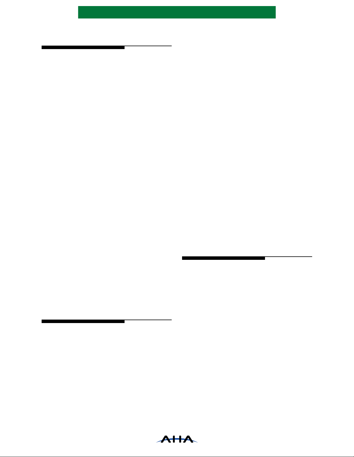
Figure 6: DMA Mode Timing for Single Word Writes, Strobe Condition of DSC=100 . . . . . . . . . . . . . . . . . . . . . . .7
Figure 7: DMA Mode Timing for Single Word Reads, Strobe Condition of DSC=100 . . . . . . . . . . . . . . . . . . . . . . .7
Figure 8: DMA Mode Timing for Four Word Burst Write, One Wait State, Strobe Condition ofDSC=100. . . . . . . .7
Figure 9: DMA Mode Timing for Four Word Burst Read, One Wait State, Strobe Condition ofDSC=100 . . . . . . .8
Figure 10: DMA Mode Timing for Eight Word Burst Write, Zero Wait State, Strobe Condition ofDSC=100. . . . . . .8
Figure 11: DMA Mode Timing for Eight Word Burst Read, Zero Wait State, Strobe Condition of DSC=100. . . . . . .8
Figure 12: FIFO Threshold Example (IFT=4, DSC=2, 1 Word Already in FIFO) . . . . . . . . . . . . . . . . . . . . . . . . . . .10
Figure 13: Request vs. End-of-Record, Strobe Condition of DSC=010. . . . . . . . . . . . . . . . . . . . . . . . . . . . . . . . . .10
Figure 14: Timing Diagram, Video Input. . . . . . . . . . . . . . . . . . . . . . . . . . . . . . . . . . . . . . . . . . . . . . . . . . . . . . . . . .12
Figure 15: Timing Diagram, Video Output . . . . . . . . . . . . . . . . . . . . . . . . . . . . . . . . . . . . . . . . . . . . . . . . . . . . . . . .12
Figure 16: Pinout . . . . . . . . . . . . . . . . . . . . . . . . . . . . . . . . . . . . . . . . . . . . . . . . . . . . . . . . . . . . . . . . . . . . . . . . . . .32
Figure 17: Data Interface Timing . . . . . . . . . . . . . . . . . . . . . . . . . . . . . . . . . . . . . . . . . . . . . . . . . . . . . . . . . . . . . . .34
Figure 18: Request Deasserts at EOR, Strobe Condition of DSC=0-3, 6-7; ERC=0. . . . . . . . . . . . . . . . . . . . . . . .34
Figure 19: Request Deasserts at EOR, Strobe Condition of DSC=0-3, 6-7; ERC=1. . . . . . . . . . . . . . . . . . . . . . . .35
Figure 20: Request Deasserts at EOR, Strobe Condition of DSC=4 or 5; ERC=0 . . . . . . . . . . . . . . . . . . . . . . . . .35
Figure 21: Request Deasserts at EOR, Strobe Condition of DSC=4 or 5; ERC=1 . . . . . . . . . . . . . . . . . . . . . . . . .35
Figure 22: Output Enable Timing. . . . . . . . . . . . . . . . . . . . . . . . . . . . . . . . . . . . . . . . . . . . . . . . . . . . . . . . . . . . . . .36
Figure 23: Video Input Port Timing. . . . . . . . . . . . . . . . . . . . . . . . . . . . . . . . . . . . . . . . . . . . . . . . . . . . . . . . . . . . . .36
Figure 24: Video Output Port Timing . . . . . . . . . . . . . . . . . . . . . . . . . . . . . . . . . . . . . . . . . . . . . . . . . . . . . . . . . . . .37
Figure 25: Microprocessor Interface Timing (PROCMODE[1]=0) . . . . . . . . . . . . . . . . . . . . . . . . . . . . . . . . . . . . . .37
Figure 26: Microprocessor Interface Timing (PROCMODE[1]=1) . . . . . . . . . . . . . . . . . . . . . . . . . . . . . . . . . . . . . .38
Figure 27: Interrupt Timing. . . . . . . . . . . . . . . . . . . . . . . . . . . . . . . . . . . . . . . . . . . . . . . . . . . . . . . . . . . . . . . . . . . .39
Figure 28: Clock Timing. . . . . . . . . . . . . . . . . . . . . . . . . . . . . . . . . . . . . . . . . . . . . . . . . . . . . . . . . . . . . . . . . . . . . .39
Figure 29: Power On Reset Timing . . . . . . . . . . . . . . . . . . . . . . . . . . . . . . . . . . . . . . . . . . . . . . . . . . . . . . . . . . . . .39
Figure A1: DMA Mode Timing for Single Word Writes, Strobe Condition of DSC=000 . . . . . . . . . . . . . . . . . . . . . .43
Figure A2: DMA Mode Timing for Single Word Reads, Strobe Condition of DSC=000 . . . . . . . . . . . . . . . . . . . . . .43
Figure A3: DMA Mode Timing for Four Word Burst Write, One Wait State, Strobe Condition ofDSC=000. . . . . . .43
Figure A4: DMA Mode Timing for Four Word Burst Read, One Wait State, Strobe Condition ofDSC=000 . . . . . .44
Figure A5: DMA Mode Timing for Eight Word Burst Write, Zero Wait State, Strobe Condition ofDSC=000. . . . . .44
Figure A6: DMA Mode Timing for Eight Word Burst Read, Zero Wait State, Strobe Condition of DSC=000. . . . . .44
Figure A7: DMA Mode Timing for Single Word Writes, Strobe Condition ofDSC=010 . . . . . . . . . . . . . . . . . . . . . .45
Figure A8: DMA Mode Timing for Single Word Reads, Strobe Condition ofDSC=010 . . . . . . . . . . . . . . . . . . . . . .45
Figure A9: DMA Mode Timing for Four Word Burst Write, One Wait State, Strobe Condition ofDSC=010. . . . . . .45
Figure A10: DMA Mode Timing for Four Word Burst Read, One Wait State, Strobe Condition ofDSC=010 . . . . . .46
Figure A11: DMA Mode Timing for Eight Word Burst Write, Zero Wait State, Strobe Condition ofDSC=010. . . . . .46
Figure A12: DMA Mode Timing for Eight Word Burst Read, Zero Wait State, Strobe Condition of DSC=010. . . . . .46
Figure A13: DMA Mode Timing for Single Word Writes, Strobe Condition of DSC=011 . . . . . . . . . . . . . . . . . . . . . .47
Figure A14: DMA Mode Timing for Single Word Reads, Strobe Condition of DSC=011 . . . . . . . . . . . . . . . . . . . . . .47
Figure A15: DMA Mode Timing for Four Word Burst Write, One Wait State, Strobe Condition of DSC=011. . . . . . .47
Figure A16: DMA Mode Timing for Four Word Burst Read, One Wait State, Strobe Condition ofDSC=011 . . . . . .48
Figure A17: DMA Mode Timing for Eight Word Burst Write, Zero Wait State, Strobe Condition ofDSC=011. . . . . .48
Figure A18: DMA Mode Timing for Eight Word Burst Read, Zero Wait State, Strobe Condition of DSC=011. . . . . .48
Figure A19: DMA Mode Timing for Single Word Writes, Strobe Condition of DSC=111 . . . . . . . . . . . . . . . . . . . . . .49
Figure A20: DMA Mode Timing for Single Word Reads, Strobe Condition of DSC=111 . . . . . . . . . . . . . . . . . . . . . .49
PS3411-0600 iii

Advanced Hardwar e Architectures, Inc.
Tables
Table 1: Data Bus and FIFO Sizes Supported by AHA3411. . . . . . . . . . . . . . . . . . . . . . . . . . . . . . . . . . . . . . . . . .2
Table 2: AHA3411 Connection to Host Microprocessors . . . . . . . . . . . . . . . . . . . . . . . . . . . . . . . . . . . . . . . . . . . .3
Table 3: Microprocessor Port Configuration . . . . . . . . . . . . . . . . . . . . . . . . . . . . . . . . . . . . . . . . . . . . . . . . . . . . . .4
Table 4: Internal Strobe Conditions for DMA Mode . . . . . . . . . . . . . . . . . . . . . . . . . . . . . . . . . . . . . . . . . . . . . . . .6
Table 5: Internal Registers . . . . . . . . . . . . . . . . . . . . . . . . . . . . . . . . . . . . . . . . . . . . . . . . . . . . . . . . . . . . . . . . . .15
Table 6: Data Port Timing Requirements . . . . . . . . . . . . . . . . . . . . . . . . . . . . . . . . . . . . . . . . . . . . . . . . . . . . . . .34
Table 7: Request vs. EOR Timing. . . . . . . . . . . . . . . . . . . . . . . . . . . . . . . . . . . . . . . . . . . . . . . . . . . . . . . . . . . . .36
Table 8: Output Enable Timing Requirements . . . . . . . . . . . . . . . . . . . . . . . . . . . . . . . . . . . . . . . . . . . . . . . . . . .3 6
Table 9: Video Input Port Timing Requirements. . . . . . . . . . . . . . . . . . . . . . . . . . . . . . . . . . . . . . . . . . . . . . . . . .36
Table 10: Video Output Port Timing Requirements . . . . . . . . . . . . . . . . . . . . . . . . . . . . . . . . . . . . . . . . . . . . . . . .37
Table 11: Microprocessor Interface Timing Requirements. . . . . . . . . . . . . . . . . . . . . . . . . . . . . . . . . . . . . . . . . . .38
Table 12: Interrupt Timing Requirements . . . . . . . . . . . . . . . . . . . . . . . . . . . . . . . . . . . . . . . . . . . . . . . . . . . . . . . .39
Table 13: Clock Timing Requirements . . . . . . . . . . . . . . . . . . . . . . . . . . . . . . . . . . . . . . . . . . . . . . . . . . . . . . . . . .39
Table 14: Power On Reset Timing Requirements. . . . . . . . . . . . . . . . . . . . . . . . . . . . . . . . . . . . . . . . . . . . . . . . . .39
iv PS3411-0600
Advanced Hardware Architectures, Inc.
1.0 INTRODUCTION
AHA3411 is a lossless compression
coprocessor IC for hardcopy systems on many
standard platforms, including PCI Bus. The device
is targeted for high throughput and high resolution
hardcopy s ystems.
Multiple record counters, higher clock
frequency, advanced banding and duplex printing
features enhance this product from the first
StarLite introduction, AHA3410. Identical
compression algori th m and simi lar firmware
considerations ease migration to this second
generation device.
Blank band generation in real time and
prearming registers between records enable
advanced banding techniqu es. Bands may be in raw
uncompressed, compressed or blank format in the
frame buffer. The device processes all three formats
and outputs the raster data to the printer engine.
Appropriate register s are prearmed when switch ing
from one type to the next. Separate byte ordering
between the Compressor and the Decompressor
with bit order control in to the compressor allow ful l
reversal of the image data for duplex printing
support. A system may use mult iple record counters
and End-of-Transfer interrupts to easily handle
pages partitioned into smaller records or bands.
This document contains f unctional des cription,
system configurations, register descriptions,
electrical characteristics and ordering information.
It is intended for system de signers considering a
compression coprocessor in their embedded
applications. Software simulation and an analysis of
the algorithm for printer and copier images of
various com plexity are also available for
evaluation. A comprehensive Designer’s Guide
complements this document to assist with the
system design. Section 1 1.0 contains a list of related
technical publications.
1.1 CONVENTIONS, NOTATIONS AND
DEFINITIONS
– Active low signals h ave an “N” appended to the
end of the signal name. For example, CSN and
RDYN.
– A “bar” over a signal name indicates an inverse of
the signal. For example, SD
of SD. This terminology is used only in logic
equations.
–“Signal assertion” means the output signal is
logically true.
– Hex values are represented with a prefix of “0x”,
such as Register “0x00”. Binary values do not
contain a prefix, for example, DSC=000.
indicates an inverse
– A range of signal names or re gister bits is denoted
by a set of colons between the numbers. Most
significant bit i s always shown first, followed by
least significant bit. For example, VOD[7:0]
indicates signal names VOD7 through VOD0.
– A logical “AND” function of two signals is
expressed with an “&” between variables.
– Mega Bytes per second is referred to as MBytes/
sec or MB/sec.
– In re ferencing micropr ocessors, an x, xx or xxx is
used as suffix to indicate more than one
processor. For example, Motorola 68xxx
processor family includes various 68000
processors from Motorola.
– Reserved bits in registers are referred as “
– REQN or ACKN ref er to either CI, DI, CO or DO
Request or Acknowledge signals, as applicable.
res”.
1.2 FEATURES
PERFORMANCE:
• 33 MBytes/sec burst rate, 33 MBytes/sec
maximum sustained
• 132 MBytes/sec burst data rate over a 32-bit data bus
• 33 MBytes/sec synchronous 8-bit video in and
video out ports
• Simultaneous compression and decompres sion at
full bandwidth
• Average 15 to 1 compression ratio for 1200 dpi
bitmap image data
• Advanced banding support: blank bands, prea rmng
FLEXIBILITY:
• Big Endian or Little Endian; 32 or 16-bit bus
width and data bit/byte reordering for duplex
printing support
• Programmable Record Lengt h, Record Count and
Scan Length Registers may be prearmed
• Scan line length up to 2K bytes
• Interfaces directly with various MIPS, Motorola
68xxx and Cold FIRE, Intel i960, and Am29K
embedded processors
• Pass-through mode passes raw data through
compression and decompression engines
• Counter checks errors in decompression
SYSTEM INTERFACE:
• Single chip compression/ decompre ssion soluti on
– no external SRAM required
• Four 16 × 32-bit FIFOs with programmable
threshold counters facilitate burst mode transfers
OTHERS:
• Low power modes
• Software emulation program available
• 128 pin quad flat package
PS3411-0600 Page 1 of 50
Advanced Hardwar e Architectures, Inc.
Figure 1: Functional Block Diagram
CIACKN
DOREQN
COREQN
DIREQN
CIREQN
SD
DOACKN
COACKN
DIACKN
(From Scanner)
VIREQN
VID[7:0]
VIACKN
D[31:0]
DRIVEN
VID
PORT
DATA
PORT
8
32
32 32
TEST
CLOCK
CLK
CI
FIFO
16x32
DI
FIFO
16x32
RSTN
DATA PORT CONTROL
8 8
PROCMODE[1:0]
COMPRESSOR
DECOMPRESSOR
MICROPROCESSO R INT ERFACE
8
PD[7:0]
1.3 FUNCTIONAL OVERVIEW
The coprocessor device has three external high
speed synchronous data ports capable of transferring
once every 33 MHz clock. These are a 32-bit
bidirectional data port, an 8-bit Video Input Data
(VID) port and a Video Output Data (VOD) port.
The 32-bit port is capable of transferring up to 132
MBytes/sec. The VID and VOD are capable of up to
33 MBytes/sec each.
The device accepts uncompressed data through
the 8-bit VID port or the 32-bit data port into its
Compression In FIFO (CI FIFO). The 32-bit data
port may be configured for 16-bit transfers.
Compressed data is available through the 32-bit data
port via the Compressed Output FIFO (CO FIFO).
The sustained data rate through the compression
engine is 33 MBytes/sec.
CO
FIFO
16x32
DO
FIFO
16x32
888
VOD
PORT
COEORN
COEOTN
(To Printer)
VOEOTN
VOEORN
VOREQN
VOD[7:0]
VOACKN
AHA3411
StarLiteTM
6
CSN
DIR
RDYN
PA[5:0]
INTRN
Decompression data may be simultaneously
processed by the device. Decompression data is
accepted through the 32-bit data port, buffered in
the Decomp ression Input FIFO (DI FIFO) and
decompressed. The output da ta is made available on
the 32-bit d ata port via the Decompres sion Output
FIFO (DO FIFO) or the 8-bit Video Output port.
The decompression engine runs on the 33 MHz
clock and is capable of processing an unco mpressed
byte every clock, i.e., 33 MB/sec.
The four FIFOs are organized as 16×32 each.
For data transfers through the three ports, the
“effective” FI FO sizes dif fer according to their data
bus widths. The table below shows the size of the
data port and the “effective” FIFO size for the
various configurations supported by the device.
Table 1: Data Bus and FIFO Sizes Supported by AHA3411
OPERATION DATA BUS WIDTH PORT EFFECTIVE FIFO SIZE
Compression Data In 8 Video In 16 x 8
Compression Data In/O ut 32 Data Port 16 x 32
Compression Data In/O ut 16 Data Port 16 x 16
Decompression Data In/Out 32 Data Port 16 x 32
Decompression Data In/Out 16 Data Port 16 x 16
Decompressed Data Out 8 Video Out 16 x 8
Page 2 of 50 PS3411-0600
Advanced Hardware Architectures, Inc.
Table 2: AHA3411 Connection to Host Microprocessors
PIN NAME i960Cx i960Kx IDT3081
PA A LAD Latched Address Latched Address
CSN
DIR
PD D LAD A/D A/D[7:0]
SD
RDYN No Connect
DRIVEN
CLOCK PCLK No Connect
Movement of data for compression or
decompression is performed using synchronous
DMA over the 32-bit data port. The Video ports
support synchronous DMA mode transfers. The
DMA strobe conditions are co nfigurabl e for the 32 bit data port depending upon the system processor
and the available DMA controller.
Data transfer for compres sion or
decompression is synchronous over the three data
ports functioning as DMA masters. To initiate a
transfer into or out of the Video ports, the device
asserts VxREQN, the external device responds with
VxACKN and begins to t ra nsf er da ta over the VID
or VOD busses on each succeeding rising edge of
the clock until VxREQN is deasserted. The 32-bit
port relies on the FIFO Threshold settings to
determine the transfer.
The sections below describe the various
configurations, programming and other special
considerations in developing a compressi on system
using AHA3411.
CS
W/R
WAIT
DEN
CS
W/R WR R/W
READY
READY
System Dependent
2.0 SYSTEM CONFIGURATION
This section provides information on
connecting AHA341 1 to variou s micro processors.
2.1 MICROPROCESSOR INTERFACE
The device is capable of interfacing directly to
various processors for embedde d application. T able 2
and Table 3 show how AHA341 1 s houl d be
connected to various host micr oprocessors.
All register accesses to AHA3411 are
performed on the 8-bit PD bus. The PD bus is the
lowest byte of the 32-bit microprocessor bus.
During reads of the internal registers, the upper 24
bits are not driven. System designers should
terminate these lines with Pullup resis tors.
the microprocesso r port. Both active high and a ctive
low write enable si gnals are al lowed a s well as two
modes for chip select. T he mode of oper atio n is set
by the PROCMODE[1:0] pins. The
PROCMODE[1] signal selects when CSN must be
active and also how long an access lasts.
determines the le ngth of the acces s. CSN must be at
least 5 clocks in length. On a read, valid data is
driven onto PD[7:0] during th e 5th clock. If CSN is
longer than 5 clocks, t hen valid data c ontinues to be
driven out onto PD[7:0]. When CSN goes inactive
(high), PD[7:0] goes tristate (asynchronously) and
RDYN is driven high as ynchronously . CSN must be
high for at least t wo clocks. RDYN is always drive n
(it is not tristated when P RO CM OD E [1 ] is high). The
mode is typical of processors such as the Motorola
68xxx.
fixed at 5 clocks, PD[7:0] is onl y driven dur ing the
fifth clock, and RDYN is driven high for the first 4
clocks and low during the fifth clock. RDYN is
tristated at all other times. Write data must be driven
the clock after CSN is sampled low. Accesses may
be back to back with no delays in between. This
mode is typical of RISC processors s uch as the i960
and Am29K.
DIR pin. If PROCMODE[0] is high, then the DIR
pin is an active low write enable. If PROCMODE[0]
is low, then the DIR pin is an active high write
enable. Figure 2 through Figure 5 illustrate the
detailed timing diagrams for the microprocessor
interface.
micropro cessors, refer to AHA Application Note
(ANDC16), Designer’ s Guide for StarLi te
Products. AHA Applications Engineering is
available to supp ort with other pr ocessors not i n the
Designer’s Guide.
System Dependent
System Dependent
System Dependent System Dependent
SYSCLK
AHA3411 provi des four modes of operat ion for
When PROCMODE[1] is high, CSN
When PROCMODE[1] is low, accesses are
PROCMODE[0] determines the polarity of the
For additional notes on interfacing to various
Motorola
MCFS102(ColdFIRE)
Decoded Chip Select
System Dependent
ACK TA
BCLOCK
TM
Family
PS3411-0600 Page 3 of 50
Advanced Hardwar e Architectures, Inc.
Table 3: Microprocessor Port Configuration
PROCMODE[1:0] DIR CYCLE LENGTH EXAMPLE PROCESSOR
00 Active high write fixed i960
01 Active low write fixed
10 Active high write variable
11 Active low write variable 68xxx, MIPS R3000
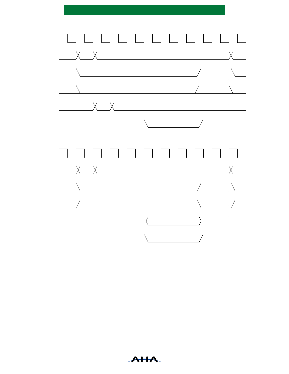
Figure 2: Microprocessor Port Write (PROCMODE[1:0]=“01”)
CLOCK
PA[5:0]
CSN
DIR
PD[7:0]
RDYN
A0
D0 D1
Figure 3: Microprocessor Port Read (PROCMODE[1:0]=“01”)
CLOCK
PA[5:0]
CSN
DIR
A0
A1
A1
A2
PD[7:0]
RDYN
D0
D1
Page 4 of 50 PS3411-0600
Advanced Hardware Architectures, Inc.
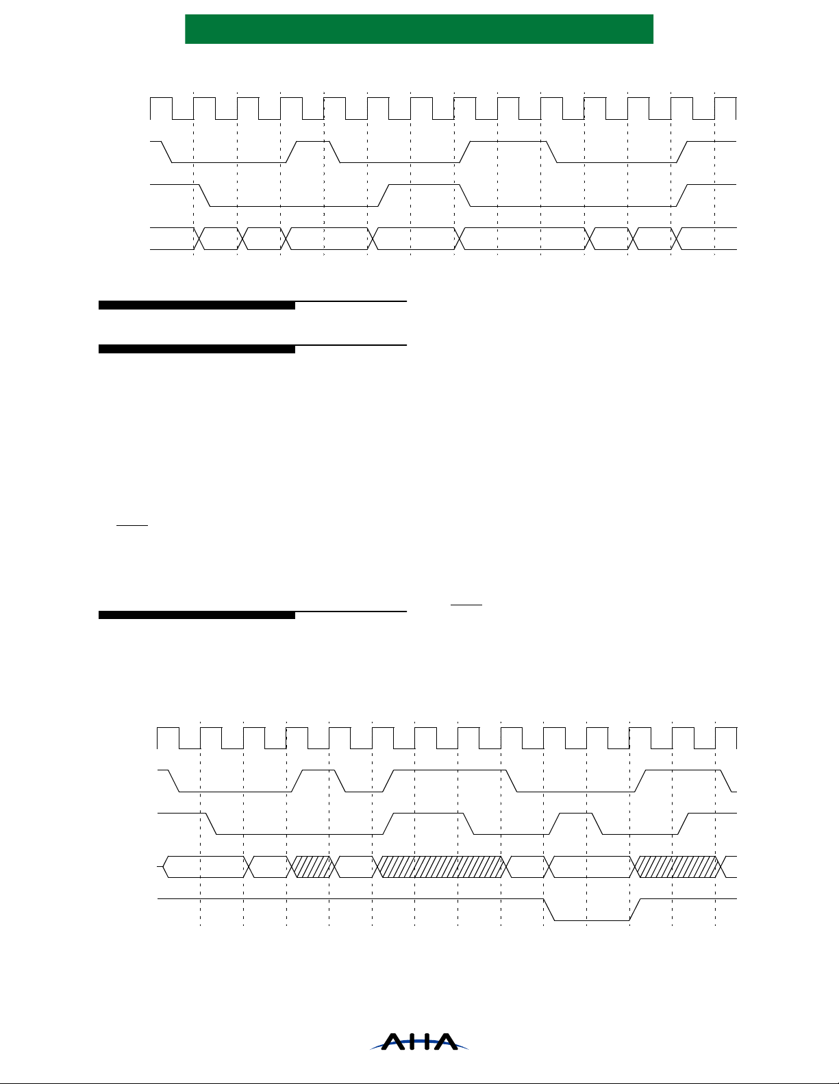
Figure 4: Microprocessor Port Write (PROCM OD E [1:0 ] = “11”)
CLOCK
PA[5:0]
CSN
DIR
PD[7:0]
RDYN
A0
D0
Figure 5: Microprocessor Port Read (PROCMODE[1:0]=“11”)
CLOCK
PA[5:0]
CSN
A0
A1
A1
DIR
PD[7:0]
RDYN
D0
PS3411-0600 Page 5 of 50
Advanced Hardwar e Architectures, Inc.
ACKN()& SD()
ACKN()& SD()
ACKN
delayed
()& SD
delayed
()
ACKN
delayed
()& SD
delayed
()
ACKN()& ACKN
delayed
()
ACKN()& ACKN
delayed
()
3.0 FUNCTIONAL DESCRIPTION
This section describes the various data ports,
special handling, data formats and clocking
structure.
3.1 DATA PORTS
AHA3411 cont ains two data input po rts, CI and
DI, and two data output ports, CO and DO on the
same 32-bit data bus, D[31:0]. Data transfers are
controlled by external DMA control. The logical
conditions under which data is written to the input
FIFOs or read from the output FIFOs are set by t he
DSC (Data Strobe Condition) field of the
Configuration 1 register.
A strobe condition defines under what logical
conditions the input FIFOs ar e written or the output
FIFOs read. CIACKN, COACKN, DIACKN,
DOACKN, and SD pins combine to strobe data in a
manner similar to DMA controllers. The DMA
Mode sub-section descr ibes t he var ious da ta st robe
options.
System
3.2 DMA MODE
On the rising edge of CLOCK when the stro be
condition is met, the port with the active
acknowledge either strobes data into or out of the
chip. No more than one port may assert
acknowledge at any one time. Table 4 shows the
various conditions that may be programmed into
register DSC.
Figure 6 through Figure 11 illustrate the DMA
mode timings for single, four word and eight word
burst transfers for DSC=100 selection. For other
DSC settings, please refer to Appe ndix A. Note that
the only differe nce between odd and eve n values of
DSC is the polarity of SD. Waveforms are only
shown for polari ties of SD correspondi ng to specific
systems.
Table 4: Internal Strobe Conditions for DMA Mode
DSC[2:0] LOGIC EQUATION SYSTEM CONFIGURATION
ACKN
)& ACKN
000
001 No specifi c system
ACKN
()& SD()
)& ACKN
()& SD()
delayed
delayed
010 General purpose DMA controller
011
100 No specifi c system
101 No specifi c system
110 No specific sy stem
111 No specific syst em
CKN
SD
i960Cx with internal DMA contro ller. SD is co nnected to
WAITN.
i960Kx with external, bus master type DMA controller.
SD is connected to RDYN.
delayed
delayed
ACKN delayed 1 clock=
SD delayed 1 cloc k=
Page 6 of 50 PS3411-0600
Advanced Hardware Architectures, Inc.
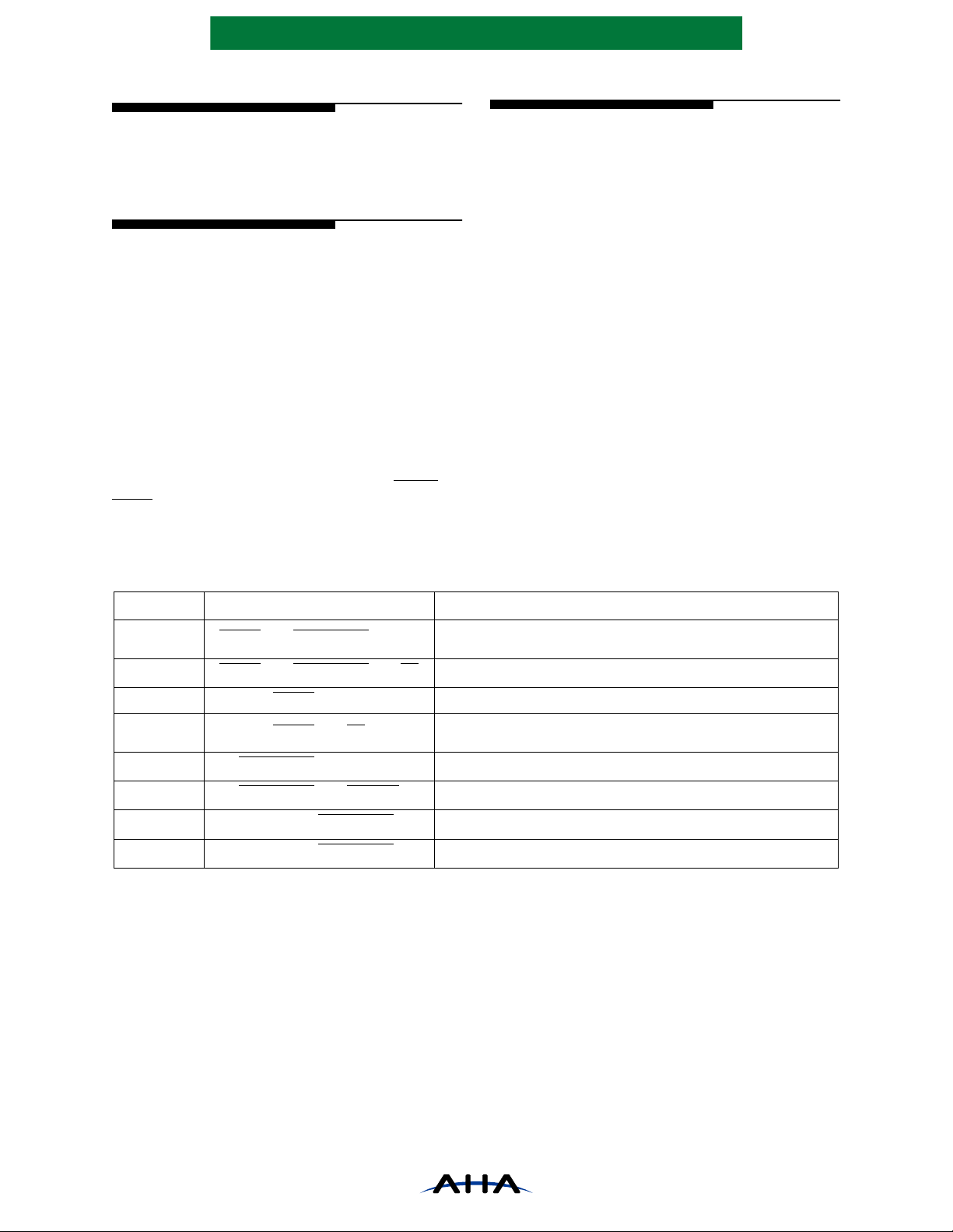
Figure 6: DMA Mode Timing for Single Word Writes, Strobe Condition of DSC=100
CLOCK
ACKN
SD
DRIVEN
D
D0 D1
Figure 7: DMA Mode Timing for Single Word Reads, Strobe Condition of DSC=100
CLOCK
ACKN
SD
DRIVEN
D
D1D0
Figure 8: DMA Mode Timing for Four Word Burst Write, One Wait State, Strobe Condition
of DSC=100
CLOCK
ACKN
SD
DRIVEN
D
D0 D2D1 D3
PS3411-0600 Page 7 of 50
Advanced Hardwar e Architectures, Inc.
Figure 9: DMA Mode Timing for Four Word Burst Read, One Wait State, Strobe Condition
of DSC=100
CLOCK
ACKN
SD
DRIVEN
D
D1D0 D2 D3
Figure 10: DMA Mode Timing for Eight Word Burst Write, Zero Wait State, Strobe Condition
of DSC=100
CLOCK
ACKN
SD
DRIVEN
D
D0 D2D1 D3 D4 D5 D6 D7
Figure 11: DMA Mode Timing for Eight Word Burst Read, Zero Wait State, Strobe Condition
of DSC=100
CLOCK
ACKN
SD
DRIVEN
D
D0 D2D1 D3 D4 D5 D6 D7
Page 8 of 50 PS3411-0600
Advanced Hardware Architectures, Inc.
3.3 PAD WORD HANDLING IN
BURST MODE
The StarLite compr ession algorit hm appends
a 15 bit End-of-Record codeword to terminate a
compression record. If a word containing an Endof-Record comes out during a bur st read, the words
following the End-of-Record are invalid (pad)
words. This prevents a burst read from crossing
record boundaries. The first word of the next burst
read is the first word of the next record. Any pad
words not previously removed must be deleted.
T wo methods are available to delete pad words.
During decompression pad words may be deleted by
using the Decompression Pause on Record
Boundaries bit (DPOR), in the Decompression
Control register. After the part is paused, the DI FIFO
must be reset by asserting the DIRST bit in the Port
Control register. Decompressor must also be reset by
asserting DDR bit in Decompression Control register.
The COEOTN signal is asserted when an End-ofRecord is present on the output of the CO FIFO and
the compression record counter has decremented to
zero, thus indicating the end of a transfer comprised
of one or more compressed records.
Another method to remove pad words during
compression is to read the Compressed Byte Count
register after pausing at an End-of-Record and
subtract this from the system’s received word count.
This difference is the number of pad words that
must be removed from the end of the compressed
record.
The COEORN signal is asserted when an Endof-Record is present on the out put of the CO FIFO.
COEORN is deasserted after the transfer. In some
systems COEORN can be used to generate a DMAdone condition if conditioned with the
acknowledge.
3.4 DMA REQUEST SIGNALS
AND STATUS
AHA3411 requests data using request pins
(CIREQN, DIREQN, CO REQN, DOR EQN ). The
requests are controlled by programmable FIFO
thresholds. Both input and output FIFOs have
programmable empty and full thresholds set in the
Input FIFO Thr esho ld
registers. By requesting only when a FIFO can sustain
a certain burst size, the bus is used more efficiently.
Operation of these request signals should not be
confused with the request signals on the video ports.
CIREQN or DIREQN active indicates space
available in the particular input FIFO, and COREQN
or DOREQN active indicates data is available in the
particular output FIFO. These request signals inactive
and Output FIFO Threshold
does not prevent data transfers. The data transfers are
controlled solely with the particular acknowledge
signal being active.
The input requests, CIREQN and DIREQN,
operate under the fol lowing priori tize d ru les, li sted
in order of highest to lowest:
1) If the FIFO reset in the
register is active, the request is inactive.
2) If a FIFO overflow interrupt is active, the
request is inactive.
3) If the FIFO is at or below the empty
threshold, the request remai ns active.
4) If the FIFO is at or above the full threshold,
the request stays inactive.
The output requests, COREQN and DOREQN,
operate under the fol lowing priori tize d ru les, li sted
in order of highest to lowest:
1) If the FIFO reset in the
register is active, the request is inactive.
2) If the output FIFO underflow interrupt is
active, the request is inactive.
3) If an EOR is pres ent in the output FIFO, th e
request goes active.
4) If the output FIFO is at or above the full
threshold, the request goes acti ve.
5) If an EOR is read (strobed) out of the FI FO,
the request goes inactive during the same
clock as the strobe (if ERC=0), otherwi se it
goes inactive on the next clock.
6) If the output FIFO i s at or below the empt y
threshold, the request goes inact ive.
Port Control
Port Control
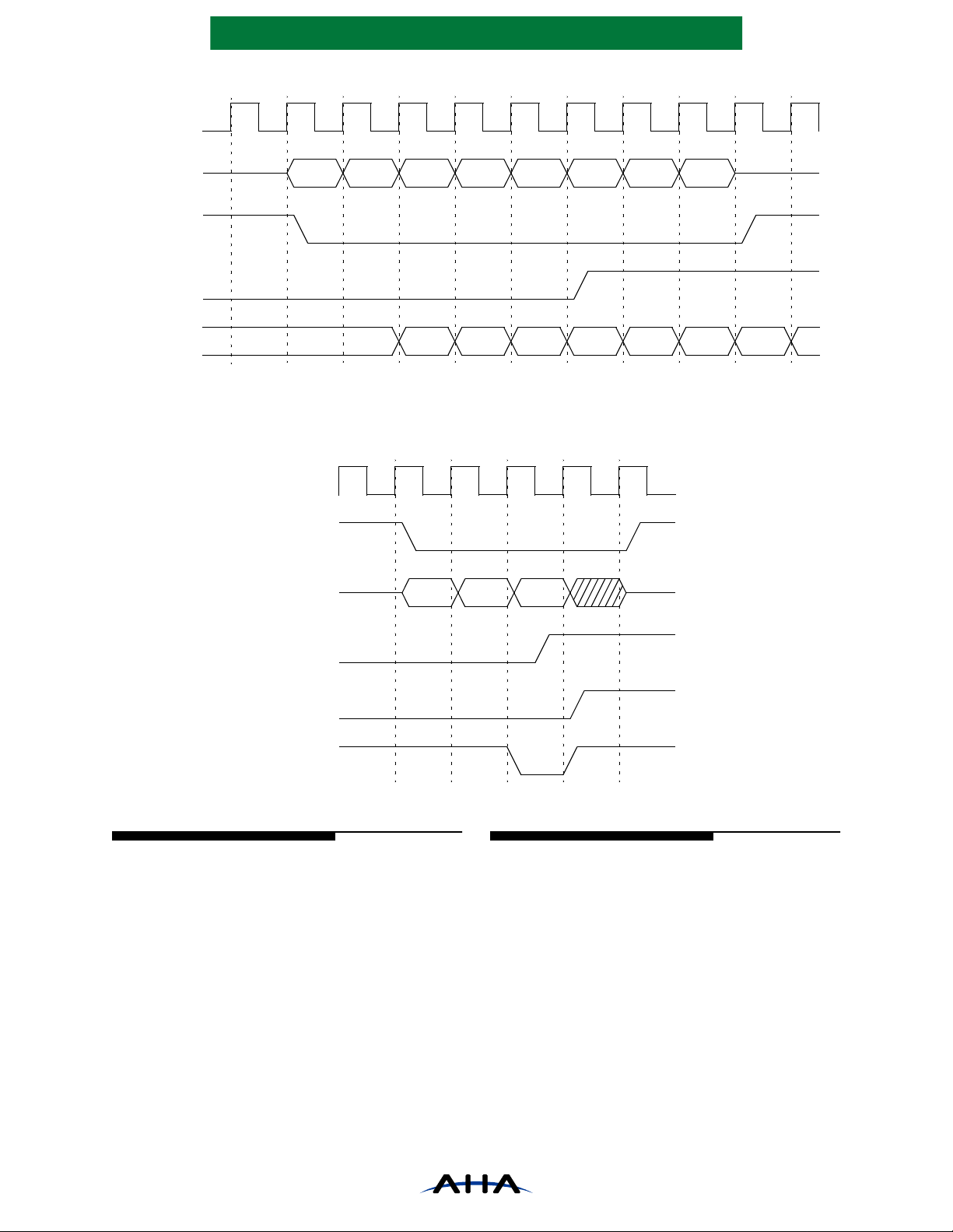
3.4.1 FIFO THRESHOLDS
For maximum efficiency, the FIFO t hresholds
should be set in such a way that the compressor
seldom runs out of data from the CI FIFO or
completely fills the output FIFO. The FIFOs are 16
words deep.
For example, in a system with fixed 8-word
bursts, good values for the thresholds are:
IET=3, IFT=4, OFT=D, OET=C
Setting the input full threshold to one higher
than the input empty threshold simply guarantees
that the request deasserts as soon as possible. The
latency between a word being strobed in and the
request changing due to a FIFO threshold condition
is 3 clocks. This should be ke p t in mi nd wh e n
programming threshold values. Refer to Section 4.0
of AHA Applicat i o n Not e ( AND C1 6) , Designer’s
Guide for StarLite
thorough discussion of FIFO thresholds. The
following figure shows an example of an input FIFO
crossing its full threshold.
TM
Family Products for a more
PS3411-0600 Page 9 of 50
Advanced Hardwar e Architectures, Inc.
Figure 12: FIFO Threshold Example (IFT=4, DSC=2, 1 Word Already in FIFO)
CLOCK
3
234
45
6
5
7
6
8
78
9
CIACKN
CIREQN
Threshold
Counter
D
1
1
2
Note: CIREQN deasserted when threshold counter exceeds IFT=4, but additional words are reading as long as
ACKN is asserted.
Figure 13: Request vs. End-of-Record, Strobe Condition of DSC=010
CLOCK
ACKN
D
EOR-2
EOR-1
EOR
REQN
(ERC=0)
REQN
(ERC=1)
EORN
3.4.2 REQUEST DURING AN END-OF-RECORD
The request deasserts at an EOR in one of two
ways. If ERC bit in System Conf igurati on 1 is zero,
the request deasserts as ynchronously during the
clock where the EOR is strobed out of the FIFO.
This leads to a lo ng output delay for REQN, but may
be necessary in some systems. For DSC values of 4
or 5, the request deasserts the first clock after the
acknowledge pulse for the EOR. If ERC is set to
one, then the request deasserts synchronously the
clock after the EOR is strobed out. The minimum
low time on the request in this case is one clock.
The request delay varies between the different
strobe conditions. See Section 8.0 AC Electrical
Specifications for further details.
3.4.3 REQUEST STATUS BITS
An externa l microproc essor can also read the
value of each reque st using the CIREQ and COREQ
bits in the Compression Port Status register and the
DIREQ and DOREQ bits in the Decompression
Port Status register. Please note the request status
bits are active high while the pins are active low.
Page 10 of 50 PS3411-0600
Advanced Hardware Architectures, Inc.
3.5 DATA FORMAT
The width of the D bus is selected with the
WIDE bit in System Configuration 0. If WIDE=1,
then D is a 32-bit bus. If WIDE=0, D is a 16-bit bus.
If the bus is configured to be 16-bits wide
(WIDE=0), all data tran sfe rs occur on D[15:0] and
the upper 16 bits of the bus, D[31:16], should be
terminated with Pullup resistors. If WIDE=0, the
FIFO is sixteen words deep.
Since the compression algorithm is byte oriented,
it is necessa ry for AHA34 1 1 t o know t he orde ring of
the bytes within the word. The COMP and DECOMP
BIG bits in System Configuration 0 select bet wee n
big endian and little endian byte ordering for the
compression and decomp re ssi on chann el. Lit tle
endian stores the first byte in the lower eight bits of a
word (D[7:0]). Big endian stores the first byte in the
uppermost eight bits of a word (D[31:24] for
WIDE=1, D[15:8] for WIDE=0) for the
decompression e ngi ne o r c ompression engin e.
REVERSE BYTE in the System Configuration
0 register allows the bit order into the compression
engine to be swapped. This control is useful for
reversing a page of data for duplex printing
applications and has no significant impact on
compression ratio performanc e.
3.6 ODD BYTE HANDLING
All data transfers to or from either the
compression or decompression engines are performed
on the D bus on word boundaries. Since no provision
is made for single byte transfers, occasionally words
will contain pad bytes. Following is a description of
when these pad bytes are necessary for each of the
data interfaces.
3.6.1 COMPRESSION INPUT AND PAD BYTES
Uncompressed data input into AHA3411 is
treated as re cords. The length of these records is
fixed by the value in the Record Length or RLEN
register. This register contains the number of
uncompressed bytes in each record. If the value in
RLEN is not an integer multiple of number of bytes
per word as selec ted by WIDE, the fi nal word in the
transfer of the record contains pad bytes. The
compression engine s imply discards these pad bytes
and has no effect on either the dictionary or the
output data stream. The next re cord must begin on a
word boundary.
The minimum value for RLEN is 4 bytes.
3.6.2 COMPRESSION OUTPUT AND
PAD BYTES
If a record ends on a byte other than the l ast byte
in a word, the final word contains 1, 2 or 3 pad bytes.
The pad bytes have a value of 0x00. Th is appli es to
the 32-bit data port only.
3.6.3 DECOMPRESSION INPUT, PAD BYTES
AND ERROR CHECKING
This port recognizes th e end of a re cord by the
appearance of a special End-of- Record sequence in
the data stream. Once this is seen, the remaining
bytes in the current word are treated as pad bytes
and discarded. The word following the end of the
record is the beginning of the next record.
When operating in decompression mode, the
Decompression R ecord Length (DRLEN) register
can be used to provid e error checking. The e xpected
length of the decompressed record is programmed
into the DRLEN register. The decompressor then
counts down from the value in DRLEN to zero.
A DERR interrupt is issued if an EOR is not
read out of the decompressor when the counter
expires or if an EOR occurs before the counter
expires (i.e., when the record length s do not match).
If the DERR interrupt is mask ed, use of the DRLEN
register is optional.
When operating in pass-t hrough mode, there is
no End-of-Record codeword for the decompressor
to see. In pass-through mode, the user must set the
record length in the DRLEN register.
3.6.4 DECOMPRESSION OUTPUT AND
PAD BYTES
When the decompressor detects an End-ofRecord codeword, it will add enough pad bytes of
value 0x00 to complete the current word as defined
by the WIDE bit in the System Configuration 0
register. For example, if a record ends on a byte
other than the last byte in a word, the final word
contains 1, 2 or 3 pad bytes. This applies to the 32bit data port only, not th e VOD port. The VOD port
never outputs pad bytes since it is 8-bits wide.
PS3411-0600 Page 11 of 50
Advanced Hardwar e Architectures, Inc.
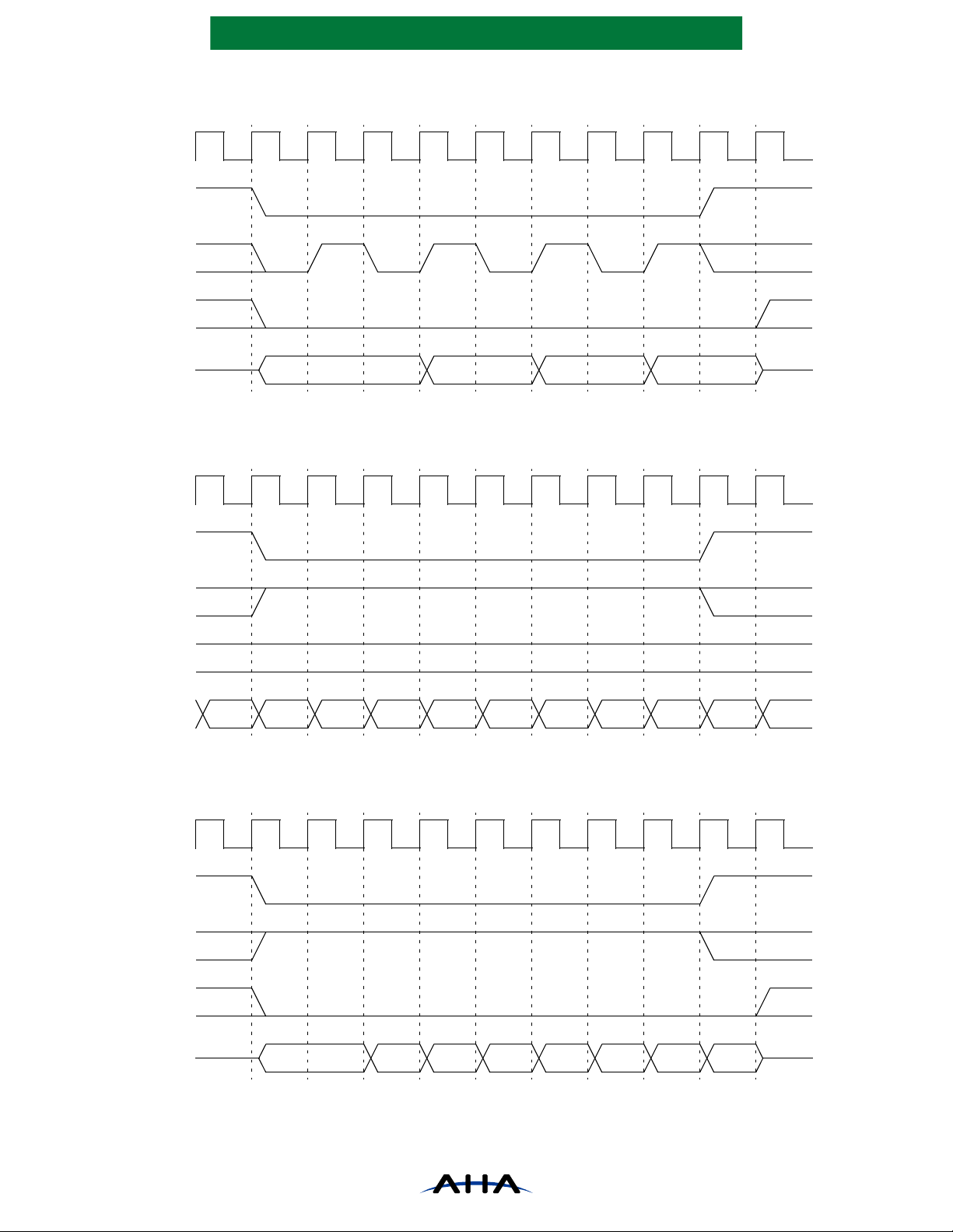
Figure 14: Timing Diagram, Video Input
CLOCK
VIREQN
VIACKN
VID[7:0]
don’t
care
0 3
1 2
3.7 VIDEO INTERFACES
3.7.1 VIDEO INPUT
The video input port is enabled by the VDIE bit
in the System Configuration 1 register . The port use s
VIREQN to indicate that the port can accept another
byte. The value on VID[7:0] is written into
AHA3411 each clock that VIREQN and VIACKN
are both low.
The video input port as serts VIREQN whenever
there is room in the CI FIFO. The value s in IET and
IFT are all ignored. Th e compressi on input FI FO is
16 bytes
transfer up to one byte per clock (33 MB/sec). The
DMA interface cannot acce ss the compression input
FIFO when VDIE is set.
3.7.2 VIDEO OUTPUT
bit in the System Configuration 1 regist er. The port
uses VOREQN to indicate that the byte on
deep in this mode. The video in put port can
The video output port is enabled by the VDOE
don’t care
4 5
VOD[7:0] is valid. An 8-bit word is re ad each clock
when both VOREQN and VOACKN are sampled
low on a rising edge of CLOCK. Pad bytes at an end
of record are discarde d by the video outp ut port and
do not appear on VOD[7:0]. When the byte on
VOD[7:0] is the last by te in a record, the VOEORN
signal goes low. To use VOEORN as an End-ofRecord indicator, it should be conditioned with
VOREQN and VOACKN. Unlike a DMA transfer,
there are no pad bytes after an End-of-Record.
VOEOTN operates similar to VOEORN. It
flags the end of an output transfer of one or more
decompressed records. VOEOTN is as ser te d when
the End-of-Record is at the out put of the DO FIFO
and the decompression record count has
decremented to zero.
The port requests whenever a valid byte is
present on the output. The values in OET and OFT
are all ignored. The decompression output FIFO is
16 bytes
deep in this mode. The video output port
can output up to one byte per clock (33 MB/sec).
The DMA interface cannot access the
decompression output FIFO when VD OE is set.
don’t
care
Figure 15: Timing Diagram, Video Output
CLOCK
VOREQN
VOACKN
VOD[7:0]
VOEORN,
VOEOTN
Page 12 of 50 PS3411-0600
0 31 2 4 5
 Loading...