

Page 1

PS3410C-0600
2365 NE Hopkins Court
Pullman, WA 99163-5601
tel: 509.334.1000
fax: 509.334.9000
e-mail: sales@aha.com
www.aha.com
advancedhardwarearchitectures
Product Specification
AHA3410C StarLite
TM
25 MBytes/sec Simultaneous Lossless Data
Compression/Decompression Coprocessor IC
Page 2

PS3410C-0600
Notes to Customers
Am29K and Fusion29K are Trademarks of Advanced Micro Devices; i960 and
Solutions 960 are T radema rks of Intel Corpo ration; ColdFIRE is a T radema rk of Motorola
Corporation.
Page 3

Advanced Hardware Architectures, Inc.
PS3410C-0600 i
Table of Contents
1.0 Introduction . . . . . . . . . . . . . . . . . . . . . . . . . . . . . . . . . . . . . . . . . . . . . . . . . . . . . . . . . . . . . . . . . . . . . . . . . . . . .1
1.1 Conventions, Notations and Definitions. . . . . . . . . . . . . . . . . . . . . . . . . . . . . . . . . . . . . . . . . . . . . . . . . . . . .1
1.2 Features . . . . . . . . . . . . . . . . . . . . . . . . . . . . . . . . . . . . . . . . . . . . . . . . . . . . . . . . . . . . . . . . . . . . . . . . . . . .1
1.3 Functional Overview . . . . . . . . . . . . . . . . . . . . . . . . . . . . . . . . . . . . . . . . . . . . . . . . . . . . . . . . . . . . . . . . . . .2
2.0 System Configuration . . . . . . . . . . . . . . . . . . . . . . . . . . . . . . . . . . . . . . . . . . . . . . . . . . . . . . . . . . . . . . . . . . . . .3
2.1 Microprocessor Interface . . . . . . . . . . . . . . . . . . . . . . . . . . . . . . . . . . . . . . . . . . . . . . . . . . . . . . . . . . . . . . . .3
3.0 Functional Description . . . . . . . . . . . . . . . . . . . . . . . . . . . . . . . . . . . . . . . . . . . . . . . . . . . . . . . . . . . . . . . . . . . .6
3.1 Data Ports . . . . . . . . . . . . . . . . . . . . . . . . . . . . . . . . . . . . . . . . . . . . . . . . . . . . . . . . . . . . . . . . . . . . . . . . . . .6
3.2 DMA Mode. . . . . . . . . . . . . . . . . . . . . . . . . . . . . . . . . . . . . . . . . . . . . . . . . . . . . . . . . . . . . . . . . . . . . . . . . . .6
3.3 Pad Word Handling in BurstMode . . . . . . . . . . . . . . . . . . . . . . . . . . . . . . . . . . . . . . . . . . . . . . . . . . . . . . . .9
3.4 DMA Request Signals andStatus. . . . . . . . . . . . . . . . . . . . . . . . . . . . . . . . . . . . . . . . . . . . . . . . . . . . . . . . .9
3.4.1 FIFO Thresholds. . . . . . . . . . . . . . . . . . . . . . . . . . . . . . . . . . . . . . . . . . . . . . . . . . . . . . . . . . . . . . . .9
3.4.2 Request During an End-of-Record. . . . . . . . . . . . . . . . . . . . . . . . . . . . . . . . . . . . . . . . . . . . . . . . .10
3.4.3 Request Status Bits . . . . . . . . . . . . . . . . . . . . . . . . . . . . . . . . . . . . . . . . . . . . . . . . . . . . . . . . . . . .10
3.5 Data Format. . . . . . . . . . . . . . . . . . . . . . . . . . . . . . . . . . . . . . . . . . . . . . . . . . . . . . . . . . . . . . . . . . . . . . . . .11
3.6 Odd Byte Handling . . . . . . . . . . . . . . . . . . . . . . . . . . . . . . . . . . . . . . . . . . . . . . . . . . . . . . . . . . . . . . . . . . .11
3.6.1 Compression Input and Pad Bytes. . . . . . . . . . . . . . . . . . . . . . . . . . . . . . . . . . . . . . . . . . . . . . . . .11
3.6.2 Compression Output and PadBytes . . . . . . . . . . . . . . . . . . . . . . . . . . . . . . . . . . . . . . . . . . . . . . .11
3.6.3 Decompression Input, Pad Bytes and Error Checking. . . . . . . . . . . . . . . . . . . . . . . . . . . . . . . . . .11
3.6.4 Decompression Output and PadBytes . . . . . . . . . . . . . . . . . . . . . . . . . . . . . . . . . . . . . . . . . . . . .11
3.7 Video Interfaces. . . . . . . . . . . . . . . . . . . . . . . . . . . . . . . . . . . . . . . . . . . . . . . . . . . . . . . . . . . . . . . . . . . . . .12
3.7.1 Video Input. . . . . . . . . . . . . . . . . . . . . . . . . . . . . . . . . . . . . . . . . . . . . . . . . . . . . . . . . . . . . . . . . . .12
3.7.2 Video Output. . . . . . . . . . . . . . . . . . . . . . . . . . . . . . . . . . . . . . . . . . . . . . . . . . . . . . . . . . . . . . . . . .12
3.8 Compression Engine. . . . . . . . . . . . . . . . . . . . . . . . . . . . . . . . . . . . . . . . . . . . . . . . . . . . . . . . . . . . . . . . . .13
3.9 Decompression Engine. . . . . . . . . . . . . . . . . . . . . . . . . . . . . . . . . . . . . . . . . . . . . . . . . . . . . . . . . . . . . . . .13
3.10 Interrupts. . . . . . . . . . . . . . . . . . . . . . . . . . . . . . . . . . . . . . . . . . . . . . . . . . . . . . . . . . . . . . . . . . . . . . . . . . .13
3.11 Low Power Mode. . . . . . . . . . . . . . . . . . . . . . . . . . . . . . . . . . . . . . . . . . . . . . . . . . . . . . . . . . . . . . . . . . . . .14
3.12 Test Mode . . . . . . . . . . . . . . . . . . . . . . . . . . . . . . . . . . . . . . . . . . . . . . . . . . . . . . . . . . . . . . . . . . . . . . . . . .14
4.0 Register Descriptions . . . . . . . . . . . . . . . . . . . . . . . . . . . . . . . . . . . . . . . . . . . . . . . . . . . . . . . . . . . . . . . . . . . .15
4.1 System Configuration 0, Address 0x00 - Read/Write . . . . . . . . . . . . . . . . . . . . . . . . . . . . . . . . . . . . . . . . .1 6
4.2 System Configuration 1, Address 0x01 - Read/Write . . . . . . . . . . . . . . . . . . . . . . . . . . . . . . . . . . . . . . . . .1 7
4.3 Input FIFO Thresholds, Address 0x02 - Read/Write. . . . . . . . . . . . . . . . . . . . . . . . . . . . . . . . . . . . . . . . . .17
4.4 Output FIFO Thresholds, Address 0x03 - Read/Write. . . . . . . . . . . . . . . . . . . . . . . . . . . . . . . . . . . . . . . . .17
4.5 Compression Ports Status, Address 0x04 - Read Only. . . . . . . . . . . . . . . . . . . . . . . . . . . . . . . . . . . . . . . .18
4.6 Decompression Ports Status, Address 0x05 - Read Only. . . . . . . . . . . . . . . . . . . . . . . . . . . . . . . . . . . . . .18
4.7 Port Control, Address 0x06 - Read/Write . . . . . . . . . . . . . . . . . . . . . . . . . . . . . . . . . . . . . . . . . . . . . . . . . .19
4.8 Interrupt Status/Control, Address 0x07 - Read/Write . . . . . . . . . . . . . . . . . . . . . . . . . . . . . . . . . . . . . . . . .19
4.9 Interrupt Mask, Address 0x09 - Read/Write . . . . . . . . . . . . . . . . . . . . . . . . . . . . . . . . . . . . . . . . . . . . . . . .20
4.10 Version, Address 0x0A - Read Only . . . . . . . . . . . . . . . . . . . . . . . . . . . . . . . . . . . . . . . . . . . . . . . . . . . . . .20
4.11 Decompression Record Length, Address 0x0C, 0x0D, 0x0E, 0x0F - Read/Write. . . . . . . . . . . . . . . . . . . .21
4.12 Record Length, Address 0x10, 0x11, 0x12, 0x13 - Read/Write . . . . . . . . . . . . . . . . . . . . . . . . . . . . . . . . .21
4.13 Compression Control, Address 0x14 - Read/Write . . . . . . . . . . . . . . . . . . . . . . . . . . . . . . . . . . . . . . . . . . .22
4.14 Compression Reserved, Address 0x15 - Read/Write . . . . . . . . . . . . . . . . . . . . . . . . . . . . . . . . . . . . . . . . .22
4.15 Compression Configuration, Address 0x16, 0x17 - Read/Write . . . . . . . . . . . . . . . . . . . . . . . . . . . . . . . . .22
4.16 Decompression Control, Address 0x18 - Read/Write . . . . . . . . . . . . . . . . . . . . . . . . . . . . . . . . . . . . . . . . .23
4.17 Decompression Reserved, Address 0x1A - Read/Write . . . . . . . . . . . . . . . . . . . . . . . . . . . . . . . . . . . . . . .23
4.18 Decompression Configuration, Address 0x1C, 0x1D - Read/Write. . . . . . . . . . . . . . . . . . . . . . . . . . . . . . .23
Page 4

Advanced Hardware Architectures, Inc.
ii PS3410C-0600
5.0 Signal Descriptions . . . . . . . . . . . . . . . . . . . . . . . . . . . . . . . . . . . . . . . . . . . . . . . . . . . . . . . . . . . . . . . . . . . . . .24
5.1 Microprocessor Interface . . . . . . . . . . . . . . . . . . . . . . . . . . . . . . . . . . . . . . . . . . . . . . . . . . . . . . . . . . . . . . .24
5.2 Data Interface . . . . . . . . . . . . . . . . . . . . . . . . . . . . . . . . . . . . . . . . . . . . . . . . . . . . . . . . . . . . . . . . . . . . . . .25
5.3 Video Interface . . . . . . . . . . . . . . . . . . . . . . . . . . . . . . . . . . . . . . . . . . . . . . . . . . . . . . . . . . . . . . . . . . . . . .26
5.4 System Control . . . . . . . . . . . . . . . . . . . . . . . . . . . . . . . . . . . . . . . . . . . . . . . . . . . . . . . . . . . . . . . . . . . . . .26
6.0 Pinout . . . . . . . . . . . . . . . . . . . . . . . . . . . . . . . . . . . . . . . . . . . . . . . . . . . . . . . . . . . . . . . . . . . . . . . . . . . . . . . . .2 7
7.0 DC Electrical Specifications . . . . . . . . . . . . . . . . . . . . . . . . . . . . . . . . . . . . . . . . . . . . . . . . . . . . . . . . . . . . . . .29
7.1 Operating Conditions. . . . . . . . . . . . . . . . . . . . . . . . . . . . . . . . . . . . . . . . . . . . . . . . . . . . . . . . . . . . . . . . . .29
7.2 Absolute Maximum Stress Ratings . . . . . . . . . . . . . . . . . . . . . . . . . . . . . . . . . . . . . . . . . . . . . . . . . . . . . . .29
8.0 AC Electrical Specifications . . . . . . . . . . . . . . . . . . . . . . . . . . . . . . . . . . . . . . . . . . . . . . . . . . . . . . . . . . . . . . .31
9.0 Package Specifications. . . . . . . . . . . . . . . . . . . . . . . . . . . . . . . . . . . . . . . . . . . . . . . . . . . . . . . . . . . . . . . . . . .38
10.0 Ordering Information. . . . . . . . . . . . . . . . . . . . . . . . . . . . . . . . . . . . . . . . . . . . . . . . . . . . . . . . . . . . . . . . . . . . .39
10.1 Available Parts. . . . . . . . . . . . . . . . . . . . . . . . . . . . . . . . . . . . . . . . . . . . . . . . . . . . . . . . . . . . . . . . . . . . . . .3 9
10.2 Part Numbering. . . . . . . . . . . . . . . . . . . . . . . . . . . . . . . . . . . . . . . . . . . . . . . . . . . . . . . . . . . . . . . . . . . . . .39
11.0 Related Publications . . . . . . . . . . . . . . . . . . . . . . . . . . . . . . . . . . . . . . . . . . . . . . . . . . . . . . . . . . . . . . . . . . . . .40
11.1 AHA Technical Publications . . . . . . . . . . . . . . . . . . . . . . . . . . . . . . . . . . . . . . . . . . . . . . . . . . . . . . . . . . . .40
11.2 Other Technical Publications. . . . . . . . . . . . . . . . . . . . . . . . . . . . . . . . . . . . . . . . . . . . . . . . . . . . . . . . . . . .40
Appendix A:Additional Timing Diagrams for DMA Mode Transfers . . . . . . . . . . . . . . . . . . . . . . . . . . . . . . . . . . .41
Page 5

Advanced Hardware Architectures, Inc.
PS3410C-0600 iii
Figures
Figure 1: Functional Block Diagram. . . . . . . . . . . . . . . . . . . . . . . . . . . . . . . . . . . . . . . . . . . . . . . . . . . . . . . . . . . . .2
Figure 2: Microprocessor Port Write (PROCMODE[1:0]=“01”). . . . . . . . . . . . . . . . . . . . . . . . . . . . . . . . . . . . . . . . .4
Figure 3: Microprocessor Port Read (PROCMODE[1:0]=“01”) . . . . . . . . . . . . . . . . . . . . . . . . . . . . . . . . . . . . . . . .4
Figure 4: Microprocessor Port Write (PROCMODE[1:0]=“11”). . . . . . . . . . . . . . . . . . . . . . . . . . . . . . . . . . . . . . . . .5
Figure 5: Microprocessor Port Read (PROCMODE[1:0]=“11”) . . . . . . . . . . . . . . . . . . . . . . . . . . . . . . . . . . . . . . . .5
Figure 6: DMA Mode Timing for Single Word Writes, Strobe Condition of DSC=100 . . . . . . . . . . . . . . . . . . . . . . .7
Figure 7: DMA Mode Timing for Single Word Reads, Strobe Condition of DSC=100 . . . . . . . . . . . . . . . . . . . . . . .7
Figure 8: DMA Mode Timing for Four Word Burst Write, One Wait State, Strobe Condition of DSC=100. . . . . . . .7
Figure 9: DMA Mode Timing for Four Word Burst Read, One Wait State, Strobe Condition of DSC=100 . . . . . . .8
Figure 10: DMA Mode Timing for Eight Word Burst Write, Zero Wait State, Strobe Condition of DSC=100. . . . . . .8
Figure 11: DMA Mode Timing for Eight Word Burst Read, Zero Wait State, Strobe Condition ofDSC=100. . . . . . .8
Figure 12: FIFO Threshold Example (IFT=4, DSC=2, 1 Word Already in FIFO) . . . . . . . . . . . . . . . . . . . . . . . . . . .10
Figure 13: Request vs. End-of-Record, Strobe Condition of DSC=010. . . . . . . . . . . . . . . . . . . . . . . . . . . . . . . . . .10
Figure 14: Timing Diagram, Video Input. . . . . . . . . . . . . . . . . . . . . . . . . . . . . . . . . . . . . . . . . . . . . . . . . . . . . . . . . .12
Figure 15: Timing Diagram, Video Output . . . . . . . . . . . . . . . . . . . . . . . . . . . . . . . . . . . . . . . . . . . . . . . . . . . . . . . .12
Figure 16: Pinout . . . . . . . . . . . . . . . . . . . . . . . . . . . . . . . . . . . . . . . . . . . . . . . . . . . . . . . . . . . . . . . . . . . . . . . . . . .28
Figure 17: Power vs. Data Rate at 25 MHz Operation. . . . . . . . . . . . . . . . . . . . . . . . . . . . . . . . . . . . . . . . . . . . . . .30
Figure 18: Data Interface Timing . . . . . . . . . . . . . . . . . . . . . . . . . . . . . . . . . . . . . . . . . . . . . . . . . . . . . . . . . . . . . . .31
Figure 19: Request Deasserts at EOR, Strobe Condition of DSC=0-3, 6-15; ERC=0. . . . . . . . . . . . . . . . . . . . . . .31
Figure 20: Request Deasserts at EOR, Strobe Condition of DSC=0-3, 6-15; ERC=1. . . . . . . . . . . . . . . . . . . . . . .32
Figure 21: Request Deasserts at EOR, Strobe Condition of DSC=4 or 5; ERC=0 . . . . . . . . . . . . . . . . . . . . . . . . .32
Figure 22: Request Deasserts at EOR, Strobe Condition of DSC=4 or 5; ERC=1 . . . . . . . . . . . . . . . . . . . . . . . . .32
Figure 23: Output Enable Timing. . . . . . . . . . . . . . . . . . . . . . . . . . . . . . . . . . . . . . . . . . . . . . . . . . . . . . . . . . . . . . .33
Figure 24: Video Input Port Timing. . . . . . . . . . . . . . . . . . . . . . . . . . . . . . . . . . . . . . . . . . . . . . . . . . . . . . . . . . . . . .34
Figure 25: Video Output Port Timing . . . . . . . . . . . . . . . . . . . . . . . . . . . . . . . . . . . . . . . . . . . . . . . . . . . . . . . . . . . .34
Figure 26: Microprocessor Interface Timing (PROCMODE[1]=0) . . . . . . . . . . . . . . . . . . . . . . . . . . . . . . . . . . . . . .35
Figure 27: Microprocessor Interface Timing (PROCMODE[1]=1) . . . . . . . . . . . . . . . . . . . . . . . . . . . . . . . . . . . . . .36
Figure 28: Interrupt Timing. . . . . . . . . . . . . . . . . . . . . . . . . . . . . . . . . . . . . . . . . . . . . . . . . . . . . . . . . . . . . . . . . . . .37
Figure 29: Clock Timing. . . . . . . . . . . . . . . . . . . . . . . . . . . . . . . . . . . . . . . . . . . . . . . . . . . . . . . . . . . . . . . . . . . . . .37
Figure 30: Power On Reset Timing . . . . . . . . . . . . . . . . . . . . . . . . . . . . . . . . . . . . . . . . . . . . . . . . . . . . . . . . . . . . .37
Figure A1: DMA Mode Timing for Single Word Writes, Strobe Condition of DSC=000 . . . . . . . . . . . . . . . . . . . . . .41
Figure A2: DMA Mode Timing for Single Word Reads, Strobe Condition of DSC=000 . . . . . . . . . . . . . . . . . . . . . .41
Figure A3: DMA Mode Timing for Four Word Burst Write, One Wait State, Strobe Condition of DSC=000. . . . . . .41
Figure A4: DMA Mode Timing for Four Word Burst Read, One Wait State, Strobe Condition of DSC=000 . . . . . .42
Figure A5: DMA Mode Timing for Eight Word Burst Write, Zero Wait State, Strobe Condition of DSC=000. . . . . .42
Figure A6: DMA Mode Timing for Eight Word Burst Read, Zero Wait State, Strobe Condition of DSC=000. . . . . .42
Figure A7: DMA Mode Timing for Single Word Writes, Strobe Condition of DSC=010 . . . . . . . . . . . . . . . . . . . . . .43
Figure A8: DMA Mode Timing for Single Word Reads, Strobe Condition of DSC=010 . . . . . . . . . . . . . . . . . . . . . .43
Figure A9: DMA Mode Timing for Four Word Burst Write, One Wait State, Strobe Condition of DSC=010. . . . . . .43
Figure A10: DMA Mode Timing for Four Word Burst Read, One Wait State, Strobe Condition of DSC=010 . . . . . .44
Figure A11: DMA Mode Timing for Eight Word Burst Write, Zero Wait State, Strobe Condition of DSC=010. . . . . .44
Figure A12: DMA Mode Timing for Eight Word Burst Read, Zero Wait State, Strobe Condition ofDSC=010. . . . . .44
Figure A13: DMA Mode Timing for Single Word Writes, Strobe Condition of DSC=011 . . . . . . . . . . . . . . . . . . . . . .45
Figure A14: DMA Mode Timing for Single Word Reads, Strobe Condition of DSC=011 . . . . . . . . . . . . . . . . . . . . . .45
Figure A15: DMA Mode Timing for Four Word Burst Write, One Wait State, Strobe Condition of DSC=011. . . . . . .45
Figure A16: DMA Mode Timing for Four Word Burst Read, One Wait State, Strobe Condition of DSC=011 . . . . . .46
Figure A17: DMA Mode Timing for Eight Word Burst Write, Zero Wait State, Strobe Condition of DSC=011. . . . . .46
Figure A18: DMA Mode Timing for Eight Word Burst Read, Zero Wait State, Strobe Condition ofDSC=011. . . . . .46
Figure A19: DMA Mode Timing for Single Word Writes, Strobe Condition of DSC=111 . . . . . . . . . . . . . . . . . . . . . .47
Figure A20: DMA Mode Timing for Single Word Reads, Strobe Condition of DSC=111 . . . . . . . . . . . . . . . . . . . . . .47
Page 6

Advanced Hardware Architectures, Inc.
iv PS3410C-0600
Tables
Table 1: Data Bus and FIFO Sizes Supported by StarLiteTM. . . . . . . . . . . . . . . . . . . . . . . . . . . . . . . . . . . . . . . . . .2
Table 2: StarLite
TM
Connection to Host Microprocessors . . . . . . . . . . . . . . . . . . . . . . . . . . . . . . . . . . . . . . . . . . . .3
Table 3: Microprocessor Port Configuration . . . . . . . . . . . . . . . . . . . . . . . . . . . . . . . . . . . . . . . . . . . . . . . . . . . . . .4
Table 4: Internal Strobe Conditions for DMA Mode . . . . . . . . . . . . . . . . . . . . . . . . . . . . . . . . . . . . . . . . . . . . . . . .6
Table 5: Internal Registers . . . . . . . . . . . . . . . . . . . . . . . . . . . . . . . . . . . . . . . . . . . . . . . . . . . . . . . . . . . . . . . . . .15
Table 6: Data Port Timing Requirements . . . . . . . . . . . . . . . . . . . . . . . . . . . . . . . . . . . . . . . . . . . . . . . . . . . . . . .31
Table 7: Request vs. EOR Timing. . . . . . . . . . . . . . . . . . . . . . . . . . . . . . . . . . . . . . . . . . . . . . . . . . . . . . . . . . . . .33
Table 8: Output Enable Timing Requirements . . . . . . . . . . . . . . . . . . . . . . . . . . . . . . . . . . . . . . . . . . . . . . . . . . .33
Table 9: Video Input Port Timing Requirements. . . . . . . . . . . . . . . . . . . . . . . . . . . . . . . . . . . . . . . . . . . . . . . . . .34
Table 10: Video Output Port Timing Requirements . . . . . . . . . . . . . . . . . . . . . . . . . . . . . . . . . . . . . . . . . . . . . . . .34
Table 11: Microprocessor Interface Timing Requirements. . . . . . . . . . . . . . . . . . . . . . . . . . . . . . . . . . . . . . . . . . .36
Table 12: Interrupt Timing Requirements . . . . . . . . . . . . . . . . . . . . . . . . . . . . . . . . . . . . . . . . . . . . . . . . . . . . . . . .37
Table 13: Clock Timing Requirements . . . . . . . . . . . . . . . . . . . . . . . . . . . . . . . . . . . . . . . . . . . . . . . . . . . . . . . . . .37
Table 14: Power On Reset Timing Requirements. . . . . . . . . . . . . . . . . . . . . . . . . . . . . . . . . . . . . . . . . . . . . . . . . .37
Page 7

PS3410C-0600 Page 1 of 47
Advanced Hardware Architectures, Inc.
1.0 INTRODUCTION
StarLite™ is a s ingle chip CMOS VLSI
coprocessor device that implements a lossless
compression and decompression algorithm. The
algorithm exhibits an average compression ratio
over 13 to 1 for bitmap image data. The device
supports simultaneous compression and decompression operations at 25 MBytes/sec each.
The device interfaces directly to various RISC
and CISC processors from AMD, Intel and
Motorola. Compression and decompression data
transfers normally occur over a high speed
bidirectional 32-bit data bus capable of up to 100
MBytes/sec synchronous data rates. Two 8-bit
synchronous video data ports provide ability to
optionally interface to scanner and print engine
respectively for applications such as multifunction
laser printers and copiers.
A low power mode is achieved by stopping all
data transfers and the clock signal. All outpu ts may
be tristated to facilitate board level testing.
This document contains functional description,
system configurations, register descriptions and
timing diagrams. It is intended for system designers
considering a compression coprocessor in their
embedded applications. Software simulation and an
analysis of the algorithm for printer and copier
images of various complexity are also available for
evaluation. A comprehensive Designer’s Guide
complementing this document is also available from
AHA to assist with the system design. Section 11.0
contains a list of related technical publications.
1.1 CONVENTIONS, NOTATIONS AND
DEFINITIONS
– Active low signals have an “N” appended to the
end of the signal name. For example, CSN and
RDYN.
– A “bar” over a signal name indicates an inverse of
the signal. For example, SD
indicates an inverse
of SD. This terminology is used only in logic
equations.
– “Signal assertion” means the output signal is
logically true.
– Hex va lues a re r eprese nted wi th a prefi x of “0x”,
such as Register “0x00”. Binary values do not
contain a prefix, for example, DSC=000.
– A rang e of signal names or register bits is denoted
by a set of colons between the numbers. Most
significant bit i s a lways shown first, foll owed by
least significant bit. For exampl e, VOD[7: 0]
indicates signal names VOD7 through VOD0.
– A logical “AND” function of two signals is
expressed with an “&” between variables.
– Mega Bytes per second is referred to as MBytes/
sec or MB/sec.
– In re ferencing microproce ssors, an x or xx is used
as suffix to indic ate more tha n one proc essor. For
example, Am290xx proces sor family includes the
Am29000, 29005, 29030 and 29035.
– Reserved bits in registers are referred as “res”.
– REQN or ACKN refer to either CI, DI, CO or DO
Request or Acknowledge signals, as applicable.
1.2 FEATURES
PERFORMANCE:
• 25 MB/sec compression and decompression rates
• 100 MB/sec burst data rate over a 32-bit data bus
• 25 MB/sec synchronous 8-bit video in and video
out ports
• Simultaneous compression and decompression
operation at full bandwidth
• Average 13 to 1 compression performance for
bitmap image data
FLEXIBILITY:
• Configura ble I/O interface for DMA mod e; Big
Endian or Little Endian; and 32-bit or 16-bit bus
widths
• Interfaces directly with Am29K or i960 family of
RISC processors and Motorola 68xxx CISC
processors
• Optional 8-bit video input and output ports
• Pass-through mode passes raw data through
compression and decompression engines
• Optional counter enables error checking in
decompression operation
SYSTEM INTERFACE:
• Single chip compression and decompression
solution
• No external SRAM required
• Four 16 × 32-bit FIFOs
• Programmable interrupts
• 25 MHz maximum clock frequency
• Output signals may be tris tated to f acilit ate board
level testing
OTHERS:
• Low power modes
• Software emulation program available
• 120 pin quad flat package
Page 8
Page 2 of 47 PS3410C-0600
Advanced Hardware Architectures, Inc.
Figure 1: Functional Block Diagram
1.3 FUNCTIONAL OVERVIEW
The coprocessor device has t hree exter nal h igh
speed synchronous data ports capable of
transferring once eve ry 25 MHz clock. These are a
32-bit bidirectional data port, an 8-bit Video Input
Data (VID) port and a Video Output Data (VOD)
port. The 32-bit port is capable of transferring up to
100 MBytes/sec. The VID and VOD are capable o f
up to 25 MBytes/sec each.
The device accepts uncompressed data through
the 8-bit VID port or the 32-bit data port in to its
Compression In FIFO (CI FIFO). The 32-bit data
port may be configured for 16-bit transfers.
Compressed data is available through the 32-bit
data port via the Compressed Output FIFO (CO
FIFO). The sustained data rate through the
compression engine is 25 MBytes/sec.
Decompression data may be simultaneously
processed by the device. Decompression data is
accepted through the 32-bit data port, buffered in
the Decompression Input FIFO (DI FIFO) and
decompressed. The output da ta is made available on
the 32-bit data port via th e Decompression Output
FIFO (DO FIFO) or the 8-bit Video Output port.
The decompression engine runs on the 25 MHz
clock and is capable of processing an unco mpressed
byte every clock, i.e., 25 MB/sec.
The four FIFOs are organized as 16 × 32 each.
For data transfers through the three ports, the
“effective” FI FO sizes differ according to the ir data
bus widths. The table below shows the size of the
data port and the “effective” FIFO size for the
various configurations supported by the device.
Table 1: Data Bus and FIFO Sizes Supported by StarLite
TM
(From Scanner)
VIREQN
VID[7:0]
VIACKN
D[31:0]
DRIVEN
TEST
CLK
RSTN
PROCMODE[1:0]
PD[7:0]
PA[4:0]
CSN
DIR
RDYN
INTRN
VOACKN
VOD[7:0]
VOREQN
VOEORN
(To Printe r )
COEORN
DOREQN
COREQN
DIREQN
CIREQN
SD
DOACKN
COACKN
DIACKN
CIACKN
VID
PORT
DATA
PORT
CI
FIFO
16x32
DI
FIFO
16x32
CLOCK
DATA PORT CONTROL
COMPRESSOR
DECOMPRESSOR
MICROPROCESSOR INTERFACE
CO
FIFO
16x32
DO
FIFO
16x32
VOD
PORT
AHA3410C
StarLiteTM
8
8 8
888
32
32 32
5
8
OPERATION DATA BUS WIDTH PORT EFFECTIVE FIFO SIZE
Compression Data In 8 Video In 16 × 8
Compressi on Data In/Out 32 Data Port 16 × 32
Compressi on Data In/Out 16 Data Port 16 × 16
Decompression Data In/Out 32 Data Port 16 × 32
Decompression Data In/Out 16 Data Port 16 × 16
Decompressed Data Out 8 Video Out 16 × 8
Page 9
PS3410C-0600 Page 3 of 47
Advanced Hardware Architectures, Inc.
Table 2: StarLiteTM Connection to Host Microprocessors
Movement of data for compression or
decompression is performed using synchronous
DMA over the 32-bit data port. The Video ports
support synchronous DMA mode transfers. The
DMA strobe conditions are co nfigurabl e for the 32 bit data port dependi ng upon the RISC proc essor of
the system and the DMA controller available.
Data transfer for compression or decompression
is synchronous over the three data ports functioning
as DMA masters. To initiate a transfer into or out of
the Video ports, the device asserts VxREQN, the
external device responds with VxACKN and begins
to transfer data over the VID or VOD busses on each
succeeding rising edge of the clock until VxREQN
is deasserted. The 32-bit port relies on the FIFO
Threshold settings to determine the transfer.
The sections below describe the various
configurations, programming and other special
considerations in developing a compressi on system
using StarLite
TM
.
2.0 SYSTEM CONFIGURATION
This section provides information on
connecting StarLi te
TM
to various microproce ssors in
DMA mode.
2.1 MICROPROCESSOR INTERFACE
The device is capable of in te rf acing directly to
various processors for embedded application. The
table below shows how StarLite
TM
should be
connected to various host microprocessors.
All register accesses to StarLite
TM
are
performed on the 8-bit PD bus. The PD bus is the
lowest byte of the 32-bit microprocessor bus.
During reads of the internal registers, the upper 24
bits are not driven. System designers should
terminate these lines with Pullup resistors.
StarLite
TM
provides four modes of ope rat ion for
the microprocessor port. Both active high and acti ve
low write enable signals are all owed a s well as two
modes for chip select . The mode of operation is set by
the PROCMODE[1:0] pins. The PROCMODE[1]
signal selects when CSN must be active and also how
long an access lasts.
When PROCMODE[1] is high, CSN determines
the length of the access. CSN must be at least 5
clocks in length. On a read, valid data is driven onto
PD[7:0] during the 5th clock. If CSN is longer than 5
clocks, then valid data continues to be driven out
onto PD[7:0]. When CSN goes inactive (high),
PD[7:0] goes tristate (asynchronously) and RDYN is
driven high asynchronously. CSN must be high for at
least two clocks. RDYN is always driven (it is not
tristated when P R OCMO D E [1] is high). The mode is
typical of processors such as the Motorola 68xxx.
When PROCMODE[1] is low, accesses are
fixed at 5 clocks, PD[7:0] is onl y driven dur ing the
fifth clock, and RDYN is driven high for the f irst 4
clocks and low during the fifth clock. RDYN is
tristated at all other times. Write data must be driven
the clock af ter CSN is sam pled low. Accesses may
be back to back with no delays in between. This
mode is typical of RISC processors s uch as the i960
and Am29K.
PROCMODE[0] determines the polarity of the
DIR pin. If PROCMODE[0] is high, then the DIR
pin is an active low write enable. If PROCMODE[0]
is low, then the DIR pin is an active high write
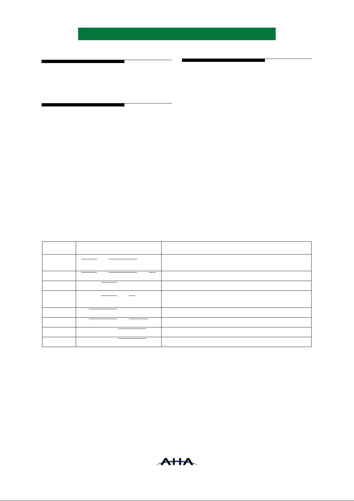
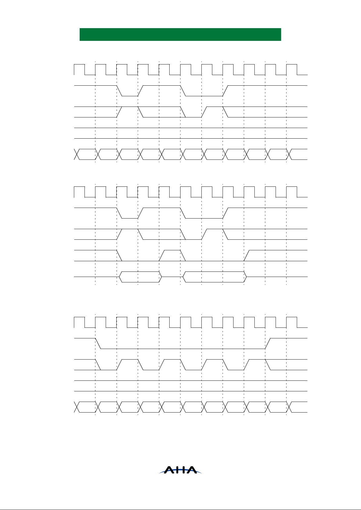
enable. Figure 2 through Figure 5 illustrate the
detailed timing diagrams for the microprocessor
interface.
For additional notes on interfacing to various
microprocessors, refer to AHA Application Note
(ANDC12), StarLite
TM
Designer’s Guide.
PIN NAME Am290xx Am292xx i960Cx i960Kx
PA A A A LAD
CSN
CS
PIACS CS CS
DIR
R/W
R/W W/R W/R
PD D ID D LAD
SD VDD VDD
WAIT
READY
RDYN
DRDY
No Connect No Connect
READY
DRIVEN System Dependent
PIAOE
DEN
System Dependent
CLOCK SYSCLK MEMCLK PCLK No Connect
Page 10
Page 4 of 47 PS3410C-0600
Advanced Hardware Architectures, Inc.
Table 3: Microprocessor Port Configuration
Figure 2: Microprocessor Port Write (PROCMODE[1:0]=“01”)
Figure 3: Microprocessor Port Read (PROCMODE[1:0]=“01”)
PROCMODE[1:0] DIR CYCLE LENGTH EXAMPLE PROCESSOR
00 Active high write fixed i960
01 Active low write fixed Am29K
10 Active high write variable
11 Active low write variable 68xxx
CLOCK
PA[4:0]
CSN
DIR
PD[7:0]
A0
RDYN
A1
D0 D1
CLOCK
PA[4:0]
CSN
DIR
PD[7:0]
A0
RDYN
A1
D0
A2
D1
Page 11
PS3410C-0600 Page 5 of 47
Advanced Hardware Architectures, Inc.
Figure 4: Microprocessor Port Write (PROCM ODE[1:0]=“11”)
Figure 5: Microprocessor Port Read (PROCMODE[1:0]=“11”)
CLOCK
PA[4:0]
CSN
DIR
PD[7:0]
A0
RDYN
A1
D0
CLOCK
PA[4:0]
CSN
DIR
PD[7:0]
A0
RDYN
A1
D0
Page 12
Page 6 of 47 PS3410C-0600
Advanced Hardware Architectures, Inc.
3.0 FUNCTIONAL DESCRIPTION
This section describes the various data ports,
special handling, data formats and clocking
structure.
3.1 DATA PORTS
StarLiteTM contains two data input ports , CI and
DI, and two data output ports, CO and DO on the
same 32-bit data bus, D[31:0]. Data transfer s can be
controlled by an exte rnal DMA control. The logical
conditions under which data is written to the input
FIFOs or read from the output FIFOs are set by t he
DSC (Data Strobe Condition) field of the System
Configuration 1 register.
A strobe condition defines under what logical
conditions the input FIFOs ar e written or the output
FIFOs read. CIACKN, COACKN, DIACKN,
DOACKN, and SD pins combine to strobe data in a
manner similar to DMA controllers. The DMA
Mode sub-section descr ibes t he variou s data strob e
options.
3.2 DMA MODE
DMA data strobes are indicated by setting the
most significant bit of the data strobe condition to
zero (DSC[3]=0).
On the rising edge of CLOCK when the strobe
condition is met, the port with the active
acknowledge either strobes data into or out of the
chip. No more than one port may assert acknowledge
at any one time. Table 4 shows the various
conditions that may be programmed into register
DSC.
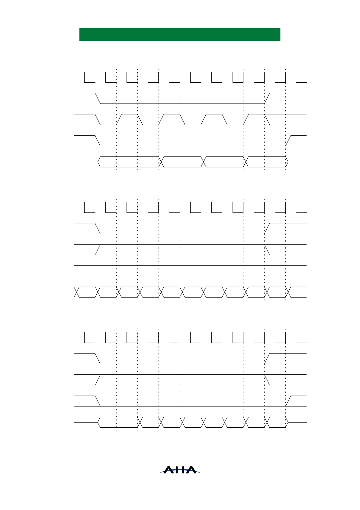
Figure 6 through Figure 11 illustrate the DMA
mode timings for single, four word and eight word
burst transfers for DSC=100 selection. For other
DSC settings, please refer to Appe ndix A. Note that
the only differe nce between odd and eve n values of
DSC is the polarity of SD. Waveforms are only
shown for polari ties of SD correspondi ng to specific
systems.
Table 4: Internal Strobe Conditions for DMA Mode
DSC[3:0] LOGIC EQUATION SYSTEM CONFIGURATION
0000
i960Cx with internal DMA contro ller. SD is connected to
WAITN.
0001 No specifi c system
0010 General purpose DMA controller
0011
i960Kx or Am290xx with extern al, bus master t ype DMA
controller. SD is connected to RDYN.
0100 Am2924x with internal DMA controller
0101 No specifi c system
0110 Am2920x with internal DMA controller
0111 Am2920x with internal DMA controller
ACKN()& ACKN
delayed
()& SD()
ACKN()& ACKN
delayed
()& SD()
ACKN()& SD()
ACKN()& SD()
ACKN
delayed
()& SD
delayed
()
ACKN
delayed
()& SD
delayed
()
ACKN()& ACKN
delayed
()
ACKN()& ACKN
delayed
()
ACKN
delayed
ACKN delayed 1 clock=
SD
delayed
SD delayed 1 clock=
Page 13
PS3410C-0600 Page 7 of 47
Advanced Hardware Architectures, Inc.
Figure 6: DMA Mode Timing for Single Word Writes, Strobe Condition of DSC=100
Figure 7: DMA Mode Timing for Single Word Reads, Strobe Condition of DSC=100
Figure 8: DMA Mode Timing for Four Word Burst Write, One Wait State, Strobe Condition
of DSC=100
CLOCK
ACKN
SD
DRIVEN
D
D0 D1
CLOCK
ACKN
SD
DRIVEN
D
D1D0
CLOCK
ACKN
SD
DRIVEN
D
D0 D2D1 D3
Page 14
Page 8 of 47 PS3410C-0600
Advanced Hardware Architectures, Inc.
Figure 9: DMA Mode Timing for Four Word Burst Read, One Wait State, Strobe Condition
of DSC=100
Figure 10: DMA Mode Timing for Eight Word Burst Write, Zero Wait State, Strobe Condition
of DSC=100
Figure 11: DMA Mode Timing for Eight Word Burst Read, Zero Wait State, Strobe Condition
of DSC=100
CLOCK
ACKN
SD
DRIVEN
D
D1D0 D2 D3
CLOCK
ACKN
SD
DRIVEN
D
D0 D2D1 D3 D4 D5 D6 D7
CLOCK
ACKN
SD
DRIVEN
D
D0 D2D1 D3 D4 D5 D6 D7
Page 15

PS3410C-0600 Page 9 of 47
Advanced Hardware Architectures, Inc.
3.3 PAD WORD HANDLING IN
BURST MODE
If a word containing an End-of-Record comes
out during a burst read, the words after the End-ofRecord are invalid (pad) words. This prevents a
burst read from crossing record boundaries. The
first word of the next burst read is the first word of
the next record. The pad words must be deleted
during decompression by usi ng the Decompressi on
Pause on Record Boundaries bit (DPOR), in the
Decompression Control register. After the part is
paused, the DI FIFO must be reset by asserting the
DIRST bit in the Port Control register.
Decompressor must als o be reset by asserting DDR
bit in Decompression Control register.
The COEORN signal is asserted when an Endof-Record is present on the output of the CO FIFO.
COEORN is active while the EOR is strobed out. In
some systems COEORN can be used to generate a
DMA-done condition.
3.4 DMA REQUEST SIGNALS
AND STATUS
StarLiteTM requests data using request pins
(CIREQN, DIREQN, COREQN, DOREQN). The
requests are controlled by programmable FIFO
thresholds. Both input and output FIFOs have
programmable empty and full thresholds set in the
Input FIFO Thres hold and Output FIFO T hreshold
registers. By requesting only when a FIFO can
sustain a ce rtain burst size, the bus is used more
efficiently.
The input requests, CIREQN and DIREQN,
operate under the following prioritized rules:
1) If the FIFO rese t in the Port Control register
is active, the request is inactive.
2) If a FIFO overflow interrupt is active, the
request is ina ctive.
3) If the FIFO is at or below the empty
threshold , the request will go active.
4) If the FIFO is a t or above the fu ll threshold,
the request will go inactiv e.
The output requests, COREQN and DOREQN,
operate under the following prioritized rules:
1) If the FIFO rese t in the Port Control register
is active, the request is inactive.
2) If the output FIFO underflow interrupt is
active, the request is inactive.
3) If an EOR is present in the output FIFO, th e
request will go active.
4) If the output FIFO is at or above the full
threshold , the request will go active.
5) If an EOR is read (strobed) out of the FI FO,
the request will go inactive during the same
clock as the strobe (if ERC=0), otherwi se it
will go inactive on the next clock.
6) If the output FIFO is at or below the empt y
threshold, the request will go inactive.
3.4.1 FIFO THRESHOLDS
For maximum efficiency, the FIFO thresholds
should be set in such a way that the compressor
seldom runs out of data from the CI FIFO or
completely fills the output FIFO. The FIFOs are 16
words deep.
For example, in a system with fixed 8-word
bursts, good values for the thresholds are:
IET=3, IFT=4, OFT=D, OET=C
Setting the input full threshold to one higher
than the input empty threshold simply guarantees
that the request will deassert as soon as possible. The
latency between a word being strobed in and the
request changing due to a FIFO threshold condition
is 3 clocks. Th i s sh o ul d be kept in mind when
programming threshold values. Refer to AHA
Application Note (ANDC12), StarLite
TM
Designer’s
Guide for a more thorough discussion of FIFO
thresholds. The following figure shows an example
of an input FIFO crossing its full threshold.
Page 16

Page 10 of 47 PS3410C-0600
Advanced Hardware Architectures, Inc.
Figure 12: FIFO Threshold Example (IFT=4, DSC=2, 1 Word Already in FIFO)
Note: CIREQN deasserted when threshold counter exceeded IFT=4.
Figure 13: Request vs. End-of-Record, Strobe Condition of DSC=010
3.4.2 REQUEST DURING AN END-OF-RECORD
The request deasserts at an EOR in one of two
ways. If ERC bit in System Configuration 1 is ‘0’,
the request will deasser t asynchronous ly during the
clock where the EOR is strobed out of the FIFO.
This leads to a lo ng output delay for REQN, but may
be necessary in some systems. For DSC values of 4
or 5, the request deasserts the first clock after the
acknowledge pulse for the EOR. If ERC is set to ‘1’,
then the request deasserts synchronously the clock
after the EOR is strobed out. The minimum low
time on the request in this case is one clock.
The request delay varies between the different
strobe conditi ons. See the timing se ction for further
details.
3.4.3 REQUEST STATUS BITS
An external microproc essor can also read the
value of each reque st using the CIREQ and COREQ
bits in the Compression Port Status register and the
DIREQ and DOREQ bits in the Decompression
Port Status register. Please note that the request
status bits are active high while the pins are active
low.
CLOCK
D
CIACKN
CIREQN
Threshold
1
2
3
45
6
7
8
1
234
5
6
78
9
Counter
EOR-2
CLOCK
D
ACKN
REQN
EOR-1
EOR
(ERC=0)
REQN
(ERC=1)
Page 17

PS3410C-0600 Page 11 of 47
Advanced Hardware Architectures, Inc.
3.5 DATA FORMAT
The width of the D bus is selected with the WIDE
bit in System Configur ati on 0. If WIDE=1, then D is
a 32-bit bus. If WIDE=0, D is a 16-bit bus. If the bus is
configured to be 16-bits wide (WIDE=0), all dat a
transfers occur on D[15:0] and the upper 16 bits of the
bus, D[31:16], should be terminated with Pullup
resistors. If WIDE=0, the FIFO is sixteen words deep.
Since the compression algorithm is byte
oriented, it i s necessary for StarLite
TM
to know the
ordering of the bytes within the word. The BIG bit
in System Configuration 0 selects between big
endian and little endi an byte orderi ng. Little endi an
stores the first byte in the lower eight bits of a word
(D[7:0]). Big endian stores the first byte in the
uppermost eight bits of a word (D[31:24] for
WIDE=1, D[15:8] for WIDE=0).
3.6 ODD BYTE HANDLING
All data transfers to or from either the
compression or decompression engines are performed
on the D bus on word boundaries. Since no provision
is made for single byte transfers, occasionally words
will contain pad bytes. Following is a description of
when these pad bytes are necessary for each of the
data interfaces.
3.6.1 COMPRESSION INPUT AND PAD BYTES
Uncompressed data input into StarLiteTM is
treated as re cords. The le ngth of these r ecords is
fixed by the value in the Record Length or RLEN
register. This register contains the number of
uncompres sed bytes in each record. If th e value in
RLEN is not an integer multiple of n umber of bytes
per word as selec ted by WIDE, the fi nal word in the
transfer of the record will contain pad bytes which
are discarded and have no effect on either the
dictionary or the output data stream. The next record
must begin on a word boundary.
The minimum value for RLEN is 4.
3.6.2 COMPRESSION OUTPUT AND
PAD BYTES
If a record ends on a byte other than the last byte
in a word, the final word will contain 1, 2 or 3 pad
bytes. The pad bytes have a value of 0x00.
3.6.3 DECOMPRESSION INPUT, PAD BYTES
AND ERROR CHECKING
This port recognizes th e end of a re cor d by the
appearance of a special End-of- Record se quence in
the data stream. Once this is seen, the remaining
bytes in the current word are treated as pad bytes
and discarded. The word following the end of the
record is the beginning of the next record.
When operating in decompression mode, the
Decompression Record Length (DRLEN) register
can be used to provid e error checking. The e xpected
length of the decompressed record is programmed
into the DRLEN register. The decompressor then
counts down from the value in DRLEN to ‘0’.
A DERR inter r upt is issued if an EOR is not
read out of the decompressor when the counter
expires or if an EOR occurs before the counter
expires (i.e., when the record length s do not match).
If the DERR interrupt is masked, us e of the DRLEN
register is optional.
When operating in pass-t hrough mode, there is
no End-of-Record codeword for the decompressor
to see. In pass-through mode, the user must set the
record length in the DRLEN register.
3.6.4 DECOMPRESSION OUTPUT AND
PAD BYTES
When the decompressor detects an End-ofRecord codeword, it will add enough pad bytes of
value 0x00 t o complete the current word.
Page 18

Page 12 of 47 PS3410C-0600
Advanced Hardware Architectures, Inc.
3.7 VIDEO INTERFACES
3.7.1 VIDEO INPUT
The video input port is enabled by the VDIE bit
in the System Configuration 1 register . The port use s
VIREQN to indicate that the port can accept another
byte. The value on VID[7:0] is written into
StarLite
TM
each clock that VIREQN and VIACKN
are both low.
The video input port as serts VIREQN whenever
there is room in the CI FIFO. The value s in IET and
IFT are all ignored. Th e compressi on input FI FO is
16 bytes
deep in this mode. The video input port can
transfer up to one byte per clock (25MB/sec). The
DMA interface cannot access t he compression input
FIFO when VDIE is set.
3.7.2 VIDEO OUTPUT
The video output por t i s enabled by the VDOE
bit in the System Configurat ion 1 regi st er. The port
uses VOREQN to indicate that the byte on
VOD[7:0] is valid. An 8-bit word is read ea ch clock
when both VOREQN and VOACKN are sampled
low on a rising edge of CLOCK. Pad bytes at an end
of record are discarde d by the video output po rt and
do not appear on VOD[7:0]. When the byte on
VOD[7:0] is the last by te in a record, the VOEORN
signal will go low. VOEORN is active while an
EOR is read out. Unlike a DMA transfer, there are
no pad bytes after an End-of-Record.
The port requests whenever a valid byte is
present on the output. The values in OET and OFT
are all ignored. The decompression output FIFO is
16 bytes
deep in this mode. The video output port
can output up to one byte per clock (25 MB/sec).
The DMA interface cannot access the
decompression output FIFO when VDOE is set.
Figure 14: Timing Diagram, Video Input
Figure 15: Timing Diagram, Video Output
CLOCK
VIREQN
VIACKN
VID[7:0]
0 3
don’t
care
1 2
don’t care
4 5
don’t
care
CLOCK
VOREQN
VOACKN
VOD[7:0]
0 31 2 4 5
VOEORN
Page 19

PS3410C-0600 Page 13 of 47
Advanced Hardware Architectures, Inc.
3.8 COMPRESSION ENGINE
The compression engine supports either
compression or pass-through processes. The
compression engine is enabled with the COMP bit
in the Compression Control register. W hen the
engine is enabled, it takes dat a from the CI FIFO as
it becomes available. This data is either compressed
by the engine or passed through unaltered. This
pass-through mode is selec ted with the CP ASS bit in
the Compression Control register. The CPASS bit
may only be changed when COMP is set to ‘0’. The
contents of the dictionary are preserved when
COMP is changed. However, when CPASS is
changed, the contents are lost. Consequently,
StarLite
TM
can not be changed from pass-through
mode to compression mode or vice versa without
losing the contents of the dictionary.
The compressor can be instructed to halt input
at the end of each record. If the CPOR bit is set, the
compressor will stop taking bytes out of the CI
FIFO immediately after th e last byte of a record. In
addition, the COMP bit will be cleared. The CEMP
bit will then indicate when all of the data has left the
compressor . Compress ion is restarte d by setting the
COMP bit.
The compression engine takes data from the
compression input FIFO at a maximum rate of 25
MBytes/sec. Two conditions cause the data rate to
drop below the maximum. The first is cause d by the
compression input FIFO running empty of data to
be compressed. The second condition is caused by
the output FIFO filling. When this occurs, the
engine halts and waits for the FIFO. While halted,
the engine goes into a low power standby mode.
Refer to the ta ble in Section 7. 1 for the extent of
power savings.
3.9 DECOMPRESSION ENGINE
The decompression engine is enabled with the
DCOMP bit in the Deco mpr ession Contr ol register .
When the engine is enabled, it takes data from the
DI FIFO as it becomes available. This dat a is either
decompressed by the engine or passed through
unaltered. Pass-through mode is selected with the
DPASS bit. DPASS may only be changed when
DCOMP is set to ‘0’ and DEMP is set to ‘1’. The
contents of the dictionary are preserved when
DCOMP is changed. However, when DPASS is
changed, the contents are lost. Consequently,
StarLite
TM
can not be changed from pass-through
mode to decompression mode or vice versa without
losing the contents of the dictionary.
The decompressor can be instructed to halt
operation at the end of each record . If the DPOR bit
is set, the decompressor will stop processing
additional data after it decodes an End-of-Record
and DCOMP will be cleared. If DPOR is set and
data from a second record enters the FIFO
immediately after the first record, bytes from the
second record will have entered the decompressor
prior to decoding the EOR. An impli cation of this is
that bytes from the second record will remain in the
decompressor and prevent DEMP from setting after
all of the data from the first record has left the
decompressor. This differs from operation of the
compression engine. In either mode, a DOEOR
interrupt is generated when the last byte of a
compressed record is read out of the chip.
The decomp ressor takes data from the
decompression input FIFO at a maximum rate of
25 MBytes/sec. StarLite
TM
can maintain this data
rate as long as th e deco mpression i nput FIFO i s not
empty or the decompression out put FIFO is not full.
3.10 INTERRUPTS
Seven conditions are reported in the Interrupt
Status/Control register as individual bits. All
interrupts are maskable by setting the corresponding
bits in the Interrupt Mask register. A ‘1’ in the
Interrupt Mask register means the corresponding bit
in the Interrupt Status/Control register is masked
and does not affect the interrupt pin (INTRN). The
INTRN pin is active whenever any unmasked
interrupt bit is set to a ‘1’.
End-of-Record interrupts are posted when a
word containing an end-of-record is strobed out of
the compression or decompression output FIFOs
(CEOR and DEOR respectively). A DEOR interrupt
is also reported if an end-of-record is read from the
video output port.
Four FIFO error conditions are also reported.
Overflowing the input FIFOs generates a CIOF or
DIOF interrupt. An ove rflow can only be cleared by
resetting the respective FIFO via the Po rt Cont rol
register.
Underflowing the output FIFOs (readi ng when
they are not ready) generates a COUF or DOUF.
Underflow interr upts are cl eared by writing a ‘1’ to
COUF or DOUF. In the event of an underflow, the
respective FIFO must be reset. Note that in systems
using fixed length bu rsts which rearbitr ate duri ng a
burst, the CO FIFO may request a nother burst when
the record actually finishes near the end of the
current burst. In this scenario a second burst takes
place causing a FIFO under flow . As long as a pause
on End-of-Record is us ed, data is not corrupted. The
FIFO simply must be reset.
Page 20

Page 14 of 47 PS3410C-0600
Advanced Hardware Architectures, Inc.
3.11 LOW POWER MODE
The AHA3410C is a data-driven sy stem. When
no data transfers are tak ing place, only the clock and
on-chip RAMs including the FIF Os re qui re power.
To reduce power consumption to its absolute
minimum, the user can stop the clock when it is
high. With the system clock stopped and at a high
level, the only current required is due to leakage.
Control and Status registers are preserved in this
mode. Reinitialization of Control registers are not
necessary when switching from Low Power to
Normal ope rating mode.
3.12 TEST MODE
In order to facilitate board level testing, the
AHA3410C provides the ability to tristate all
outputs. When the TEST pin is high, all outputs of
the chip are tristated. When test is low, the chip
returns to normal operation.
Page 21

PS3410C-0600 Page 15 of 47
Advanced Hardware Architectures, Inc.
4.0 REGISTER DESCRIPTIONS
The microprocessor configures, controls and monitors IC operation through the use of the registers
defined in this section. All write registers are readable with the exception of Record Length registers. All
registers are reset to ‘0’ on RSTN unless otherwise s t ated. The bits labeled “res” are reserved and mu st be
set to ‘0’ when writing to registers unless otherwise noted.
A summary of registers is listed below.
Table 5: Internal Registers
ADDRESS R/W DESCRIPTION FUNCTION
DEFAULT
AFTER RSTN
00 R/W System Configuration 0
Big Endian vs. Little Endian, 32bit vs. 16-bit
Undefined
01 R/W System Configuration 1
Data Strobe Condition, EOR
Request Control, VDO Port
Enable, VDI Port Enable
0x00
02 R/W Input FIFO Thresholds
Input FIFOs Empty Threshold,
Full Threshold
Undefined
03 R/W Output FIFO Thresholds
Output FIFOs Empty Threshold,
Full Threshold
Undefined
04 R Compression Ports Status
FIFO Status, Reque st Status , EOR
Status
Undefined
05 R Decompression Ports Status
FIFO Status, Reque st Status , EOR
Status
Undefined
06 R/W Port Control Reset Individual FIF Os 0x0F
07 R/W Interrupt Status/Control EOR, Overflow, Underflow 0x00
09 R/W Interrupt Mask Interrupt Mask bits 0xFF
0A R Version Die Version Number 0x21
0C R/W
Decompression Record
Length 0
Bytes Remaining in Transfer,
Byte 0
0xFF
0D R/W
Decompression Record
Length 1
" " , Byte 1 0xFF
0E R/W
Decompression Record
Length 2
" " , Byte 2 0xFF
0F R/W
Decompression Record
Length 3
" " , Byte 3 0xFF
10 R/W Record Length 0
Length of Uncompressed Data in
Bytes, Byte 0
Undefined
11 R/W Record Length 1 " " , Byte 1 Undefined
12 R/W Record Length 2 " " , Byte 2 Undefined
13 R/W Record Length 3 " " , Byte 3 Undefined
14 R/W Compression Control
Pause on Record Boundaries,
Enable Compression, Com pression Engine Empty Status, Compression Dictionary Reset, Select
Pass-Through Mode
0x04
15 R/W Compression Reserved For Production Testing Only 0x00
16 R/W Compres sion Configuration 0 Line Length Register Lower 8 bits Undefined
17 R/W Compression Configuration 1 Line Length Register Upper 3 bits Undefined
Page 22

Page 16 of 47 PS3410C-0600
Advanced Hardware Architectures, Inc.
4.1 SYSTEM CONFIGURATION 0, ADDRESS 0x00 - READ/WRITE
This register is not cleared by reset and must be initialized prior to any data t ransfer.
X
WIDE - Selects between 32 and 16-bit D buses.
BIG - Select between little and big endian data orders . The lea st signi fi cant bit in a byte is always in
position ‘0’.
18 R/W Decompression Control
Pause on Record Boundaries,
Enable Decompression Engine,
Decompression Engine Empty
Status, Dictionary Reset, Enable
Pass-Through Mode
0x04
1A R/W Decompression Reserved For Production Testing Only 0x00
1C R/W Decompression Configuration 0 Line Length Register Lower 8 bits Undefined
1D R/W Decompression Configuration 1 Line Length Register Upper 3 bits Undefined
Address
(hex)
bit7 bit6 bit5 bit4 bit3 bit2 bit1 bit0
00 BIG WIDE res res
BIG WIDE DESCRIPTION
0 0 Little Endian data order 16-bit words
D[15:8] D[7:0]
Byte 1 Byte 0
0 1 Little Endian data order 32-bit words
D[31:24] D[23:16] D[15:8] D[7:0]
Byte 3Byte 2Byte 1Byte 0
1 0 Big Endian data order 16-bit words
D[15:8] D[7:0]
Byte 0 Byte 1
1 1 Big Endian data order 32-bit words
D[31:24] D[23:16] D[15:8] D[7:0]
Byte 0Byte 1Byte 2Byte 3
ADDRESS R/W DESCRIPTION FUNCTION
DEFAULT
AFTER RSTN
Page 23

PS3410C-0600 Page 17 of 47
Advanced Hardware Architectures, Inc.
4.2 SYSTEM CONFIGURATION 1, ADDRESS 0x01 - READ/WRITE
This register is cleared by reset.
DSC[3:0] - Data Strobe Condit ion. Control the condition used to str obe da ta into and out of the data ports
on the D bus. Table 4 shows the programming for the strobe condition for DMA data transfer
modes.
ERC - EOR Request Control. Determines when COREQN and DOREQN deassert at an End-of-
Record. If ERC=0 then t he re que st dea ssert s asy nchrono usly d uring th e cloc k when a n EOR is
strobed out. If ERC=1 then the request deasserts synchronously the clock after an EOR is
strobed out. See Figure 19.
VDOE - VDO Port Enable. When this bit is set, the data from the decompression output FIFO goes to
the VDO port. When the bit is clear, the decompressed data is read by DMA on the D bus.
VDIE - VDI Port Enable. When this bit is set, the VDI po rt will handsha ke data and wri te it into the
compression input FIFO. When the bit is clea r , the compressi on input FIFO is wri tten by DMA
from the D bus.
4.3 INPUT FIFO THRESHOLDS, ADDRESS 0x02 - READ/WRITE
This regist er is readable and writable. After reset, it s contents are undefined. It must be wri t ten before
any input or output data movement may be performed.
IET[3:0] - Empty threshold for input FIFOs. If the number of words in the input FIFO (CI or DI) is less
than or equal to this number, the re quest for that channel will be asserted.
IFT[3:0] - Full threshold for input FIFOs. If the number of words in the input FIFO (CI or DI) is greater
than or equal to this number, the request for the channel is deasserted.
4.4 OUTPUT FIFO THRESHOLDS, ADDRESS 0x03 - READ/WRITE
This regist er is readable and writable. After reset, it s contents are undefined. It must be wri t ten before
any input or output data movement may be performed.
OET[3:0] - Empty threshold for outp ut FIFOs. If the number of wo rds in the output FIFO (CO or DO) is
less than or equal to this number, the request for the channel will be deasserted (except in the
case of an End-of-Record).
OFT[3:0] - Full threshold for output FIFOs. If the number of words in the output FIFO (CO or DO) is
greater than or equal to this number, the request for that channel will be asserted.
Address
(hex)
bit7 bit6 bit5 bit4 bit3 bit2 bit1 bit0
01 res VDIE VDOE ERC DSC[3:0]
Address
(hex)
bit7 bit6 bit5 bit4 bit3 bit2 bit1 bit0
02 IFT[3:0] IET[3:0]
Address
(hex)
bit7 bit6 bit5 bit4 bit3 bit2 bit1 bit0
03 OFT[3:0] OET[3:0]
Page 24

Page 18 of 47 PS3410C-0600
Advanced Hardware Architectures, Inc.
4.5 COMPRESSION PORTS STATUS, ADDRESS 0x04 - READ ONLY
This is a read only register. Writing to this register has no ef fect . After re set, its content s are undef ined.
CIFT - Compression input FIFO full threshold. This signal is active when t he CI FI FO is g rea ter than
or equal to the programmed FIFO full threshold. After reset and the Input FIFO Threshold
register has been written, this bit contains a ‘0’.
CIREQ - Compression input request signal state. Reports the current state for the CIREQN pin. Notice
that this bit is active high while the pin is active low. Therefore, the value of this bit will always
be the inverse of the value of the signal. After reset this bit contains a ‘0’.
COET - Compres sion output FIFO em pty threshold. Thi s signal is active whe n the CO FIFO is less th an
or equal to the programmed FIFO emp ty threshold. Aft er reset and the Outpu t FIFO Thr eshold
register has been written, this bit contains a ‘1’.
COREQ - Compression output request signal state. Repor ts the current stat e for the COREQN pin. Notice
that this bit is active high while the pin is active low. Therefore, the value of this bit will always
be the inverse of the value of the signal. After reset this bit contains a ‘0’.
COEOR - Compression output end of record. This s ignal is activ e when the output FIFO contains the end-
of-record code. After reset this bit contains a ‘0’.
CIEMP - Compression input empty. This bit is active when the CI FIFO is empty. After reset this bit
contains a ‘1’.
COEMP - Compression output empty. This bit is active when the CO FIFO is empty. After reset this bit
contains a ‘1’.
4.6 DECOMPRESSION PORTS STATUS, ADDRESS 0x05 - READ ONLY
This is a read only register. Writing to this register has no ef fect . After re set, its content s are undef ined.
DIFT - Decompression input FIFO f ull thres hold. This s ignal is act ive when the DI FIFO is at or above
the programmed FIFO full threshold. After reset and the Input FIFO Threshold register has
been written, this bit contains a ‘0’.
DIREQ - Decompression input request signal st ate. Reports the current stat e for the DIREQN pin. Notice
that this bit is active high while the pin is active low. Therefore, the value of this bit will always
be the inverse of the value of the signal. After reset this bit contains a ‘0’.
DOET - Decompression output FIFO empty threshold. This si gnal i s ac ti ve wh en t he DO FIFO is at or
below the programmed FIFO empty threshold. After reset and the Output FIFO Threshold
register has been written, this bit contains a ‘1’.
DOREQ - Decompression output request signal state. Reports the current state for the DOREQN pin.
Notice that this bit is act ive high while the pi n is active low. Therefore, the value of this bit will
always be the inverse of the value of the signal. After reset this bit contains a ‘0’.
DOEOR - Decompression output end of record. This signal is active when the output FIFO contains the
End-of-Record code. After reset this bit contains a ‘0’.
DIEMP - Decompression input empty. This bit is active when the DI FIFO is empty. After reset this bit
contains a ‘1’.
DOEMP - Dec ompression output empty. This bit is active when the DO FIFO is empty. After reset this bit
contains a ‘1’.
Address
(hex)
bit7 bit6 bit5 bit4 bit3 bit2 bit1 bit0
04 COEMP CIEMP res COEOR COREQ COET CIREQ CIFT
Address
(hex)
bit7 bit6 bit5 bit4 bit3 bit2 bit1 bit0
05 DOEMP DIEMP res DOEOR DOREQ DOET DIREQ DIFT
Page 25

PS3410C-0600 Page 19 of 47
Advanced Hardware Architectures, Inc.
4.7 PORT CONTROL, ADDRESS 0x06 - READ/WRITE
This regist er is initialized to ‘0F’ afte r reset.
CIRST - Compression input reset . Setting this bit to a ‘1’ reset s the CI FIFO and clears stat e machines on
the compression input port. The reset condition will remain active until the microprocessor
writes a ‘0’ to this bit.
CORST - Compression output reset. Setting thi s bit to a ‘1’ resets the CO FIFO and clear s state machine s
on the compression output port . The reset condition wil l remain active until the mic roprocessor
writes a ‘0’ to this bit.
DIRST - Decompression input reset. Setting this bit to a ‘1’ resets the DI FIFO and clears the state
machines in the decompression input port. The reset condition will remain active until the
microprocessor writes a ‘0’ to this bit.
DORST - Decompression output reset. Setting this bit to a ‘1’ resets the DO FIFO and clears the state
machines in the decompression output port. The reset condition will remain active until the
microprocessor writes a ‘0’ to this bit.
4.8 INTERRUPT STATUS/CONTROL, ADDRESS 0x07 - READ/WRITE
This regist er is initialized to ‘00’ afte r reset.
CEOR - Compression End-of-Record interrupt. This bit is set when an End-of-Record codeword is
strobed out of the compression output port. To clear this interrupt the microprocessor must
write a ‘1’ to this bit.
DEOR - Decompression End-of-Recor d interrupt. This bit is set when the last byte of a recor d is strobed
out of the decompress ion DMA or vid eo output por t. To clear this interrupt the micr oprocesso r
must write a ‘1’ to this bit.
DERR - Decompression Error. This bit is set if an EOR leaves the decompressor before DRLEN has
counted down to zero or if DRLEN counts to zero and the last byte is not an EOR. DERR is
only active in decompression mode (DPASS=0). To clear this interrupt, the microprocessor
must write a ‘1’ to this bit.
CIOF - Compression Input FIFO Ov erf lo w. This interrupt is generated when a wri t e to the CI FIFO is
performed when it is full. Al l data written when the FIFO is full is lost. T he only means of
recovery from this error is to reset the FIFO with the CIRST bit. Resetting the FIFO causes this
interrupt to clear. While the interrupt is set CIREQN is inactive.
DIOF - Decompr ession Input FIFO Overfl ow. This interrupt is generated when a write to the DI FIFO
is performed when it is full. All data written when the FIFO is full is lost. The only means of
recovery from this error is to reset the FIFO with the DIRST bit. Resetting the FIFO causes this
interrupt to clear. While the interrupt is set DIREQN is inactive.
Address
(hex)
bit7 bit6 bit5 bit4 bit3 bit2 bit1 bit0
06 res DORST DIRST CORST CIRST
Address
(hex)
bit7 bit6 bit5 bit4 bit3 bit2 bit1 bit0
07 DOUF COUF DIOF CIOF res DERR DEOR CEOR
Page 26

Page 20 of 47 PS3410C-0600
Advanced Hardware Architectures, Inc.
COUF - Compression Output FIFO underflow. This interrupt is generated when a read from the CO
FIFO is performed when it is empty. Once this interrupt is set, the CO FIFO must be reset with
the CORST bit. To clear this interrupt the microproce ssor must write a ‘1’ to this bit. While the
interrupt is set, COREQN is inactive.
DOUF - Decompression Output FIFO underflow. This interrupt is generated when a read from the DO
FIFO is performed when it is empt y. Once this interrupt is set, the DO FIFO must be reset wi th
the DORST bit. T o clear this interru pt the microprocess or must write a ‘1’ to this bit. While the
interrupt is set, DOREQN is inactive.
4.9 INTERRUPT MASK, ADDRESS 0x09 - READ/WRITE
This regist er is initialized to ‘FF’ after reset.
CEORM - Compression End-of -Recor d Inter rupt Mas k. When set to a ‘1’, prev ents Compr essio n End-of -
Record from causing INTRN to go active.
DEORM - Decompression End-of-Record Interrupt Mask. When set to a ‘1’, prevents Decompression
End-of-Record from causing INTRN to go active.
DERRM - Decompression Error Mask. When set to a ‘1’, prevents a decompression error (DERR) from
causing INTRN to go active.
CIOFM - Compression Input FIFO Overflow Mask. When set to a ‘1’, prevents a compression input
FIFO overflow (CIOF) from causing INTRN to go active.
DIOFM - Decompression Input FIFO Overflow Mask. Whe n set to a ‘1’, prevents a decompression i nput
FIFO overflow (DIOF) from causing INTRN to go active.
COUFM - Compression Output FIFO Underf low Mask. When set t o a ‘1’, prevent s a compressi on outpu t
FIFO underflow (COUF) from causing INTRN to go active.
DOUFM - Decompression Output FIFO Underflow Mask. When set to a ‘1’, prevents a decompression
output FIFO underflow (DOUF) from causing INTRN to go active.
4.10 VERSION, ADDRESS 0x0A - READ ONLY
This is a read only register. Writing to this register has no effect on IC operation.
VERSION[7:0] - Contains version number of the die. Initial version is 0x21.
Address
(hex)
bit7 bit6 bit5 bit4 bit3 bit2 bit1 bit0
09 DOUFM COUFM DIOFM CIOFM res DERRM DEORM C EORM
Address
(hex)
bit7 bit6 bit5 bit4 bit3 bit2 bit1 bit0
0A VERSION[7:0]
Page 27

PS3410C-0600 Page 21 of 47
Advanced Hardware Architectures, Inc.
4.11 DECOMPRESSION RECORD LENGTH, ADDRESS 0x0C, 0x0D, 0x0E, 0x0F -
READ/WRITE
These registers are initialized to ‘FF’ after reset.
DRLEN[31:0]-Decompression Record Length. Contains the number of bytes in a decompressed record.
These registers provide different functions depending on whether the decompressor is in passthrough or decompression mode. In decompress mode, the data itself contains EOR
information and DRLEN is only used for error checking. DRLEN is decremented each time a
byte leaves the decompressor.
In decompression mode, a DERR interrupt is issued if an EOR is not read out of the
decompressor when the counter expires or if an EOR occurs before the counter expires (i.e.,
when the record lengths do not match). If the DERR interrupt is masked, use of the DRLEN
register is optional in decompression mode.
In pass-through mode, DRLEN determines the size of records read out of the decompressor.
The counter is decremented for each byte read into the decompressor.
In either mode, the counter reloads when it reaches zero or when DRLEN[31:24] is written.
Reading DRLEN returns the number of bytes left in the count.
4.12 RECORD LENGTH, ADDRESS 0x10, 0x11, 0x12, 0x13 - READ/WRITE
These registers are undefined after reset.
RLEN[31:0]- Record Length. Length of an uncompressed record in bytes. Writing these addresses sets a
register containi ng the l ength of a reco rd. Readi ng thes e addre sses re tu rns a co unter i ndica ting
the number of bytes remaining in the current record. The counter is decremented each time a
byte leaves the CI FIFO. The counter automatically reloads from the register at the end of a
record. The counter is also reloaded when RLEN[31:24] is written. The record length register
is also valid during pass-through operation.
The minimum value for RLEN is 4.
Address
(hex)
bit7 bit6 bit5 bit4 bit3 bit2 bit1 bit0
0C DRLEN[7:0]
0D DRLEN[15:8]
0E DRLEN[23:16]
0F DRLEN[31:24]
Address
(hex)
bit7 bit6 bit5 bit4 bit3 bit2 bit1 bit0
10 RLEN[7:0]
11 RLEN[15:8]
12 RLEN[23:16]
13 RLEN[31:24]
Page 28

Page 22 of 47 PS3410C-0600
Advanced Hardware Architectures, Inc.
4.13 COMPRESSION CONTROL, ADDRESS 0x14 - READ/WRITE
This regist er is initialized to ‘04’ afte r reset.
CPOR - Compression Pause on record boundaries. When this bit is set to ‘1’, the compressor stops
taking data from the input FIFO once a record boundary is found. A record boundary is
indicated by the RLEN r egister dec rementing to ‘0’. Upon finding the r ecord boundary, COMP
is cleared. This bit may only be changed when COMP is set to ‘0’. After system reset , this bit
is cleared.
COMP - Compression. Setting this bit to a ‘1’ enables the data compression engine (or pass-through mode
if CP ASS is set) to take data from the compression input FIFO. If this bit is cleared, compression
stops. The bit is automatically cleared at the end of a record if CPOR is set. The compression can
be restarted without loss of data by setting COMP. After reset, this bit is cleared.
CEMP - Compression engine empty. This bit is set to a ‘1’ when no data is present inside the
compressor. Writing to this bit has no effect. After system re set, this bit is set.
CDR - Compression Dictionary Reset. Sett ing this bit immedi ately resets the compressor including the
compression dictionar y. The reset condition will remain active unt il th e micr oproce ssor wri tes
a ‘0’ to this bit.
CPASS - Compression pass-through mode. While this bit is set, data is passed directly through the
compression engine without any effect on either the dictionary or the data itself. This bit may only
be changed when compression is disabled (COMP=0) and the compression engine is empty of
data (CEMP=0). The pass-through operation is started by setting COMP. To stop the passthrough operation, COMP should be cleared (to pause operation) and then CPASS may be
cleared.
bit[5] - Reserved. Set to ‘0’.
bit[7:6] - Reserved. Set to ‘0’.
4.14 COMPRESSION RESERVED, ADDRESS 0x15 - READ/WRITE
This register is used for production testing. Must be written with ‘0’ if at all. Resets to ‘0’.
4.15 COMPRESSION CONFIGURATION, ADDRESS 0x16, 0x17 - READ/WRITE
This register contains information necessary for the compression operation. It must be set prior to any
compression operatio n. It shou ld only be changed whe n COMP is cleare d and CEMP is set. Afte r changin g
compression configurat ion , the comp resso r should be reset us ing CDR. These regis ters are unde fi ned aft er
reset.
LINE[10:0]-Line length. The number of bytes in the scan line is programmed here. Minimum value is 16.
Address
(hex)
bit7 bit6 bit5 bit4 bit3 bit2 bit1 bit0
14 res CPASS CDR CEMP COMP CPOR
Address
(hex)
bit7 bit6 bit5 bit4 bit3 bit2 bit1 bit0
15 res
Address
(hex)
bit7 bit6 bit5 bit4 bit3 bit2 bit1 bit0
16 LINE[7:0]
17 res LINE[10:8]
Page 29

PS3410C-0600 Page 23 of 47
Advanced Hardware Architectures, Inc.
4.16 DECOMPRESSION CONTROL, ADDRESS 0x18 - READ/WRITE
This regist er is initialized to ‘04’ afte r reset.
DPOR - Decompression Pause on record bound aries. When this bit is set to ‘1’, the deco mpressor stops
taking data from the input FIFO once a record boundary is found. Upon finding the record
boundary, DCOMP is cleared. This bit may only be ch anged when DCOMP is se t to ‘0’. After
system reset or DDR, this bit is cleared.
DCOMP - Decompression. Setting this bit to a ‘1’ enables the decompression engine (or pass-through
mode if DPASS is set) to take data from the decompression input FIFO. If this bit is cleared,
decompression stops. The bit is automatically cleared at the end of a record if DPOR is set.
Decompression can be rest arted without loss of d ata by s et ti ng DCOMP. After system rese t or
DDR, this bit is cleared.
DEMP - Decompression engine empty . Thi s bit is set when the decompression e ngine is cleared of data.
Writing to this bit has no effect. After system reset, this bit is set.
DDR - Decompression Dictionary Reset. Setting this bit immediately resets the decompressor
including the decompression dictionary. The reset condition will remain active until the
microprocessor writes a ‘0’ to this bit.
DPASS - Decompression pass-through mode. While this bit is set, data is passed directly through the
decompression engine without any effect on the data. This bit may only be changed when
decompression is disabled (DCOMP=0) and the decompression engine is empty of data
(DEMP=1). The pass-th rough operat ion is sta rted by sett ing DCOMP. T o stop t he pass-through
operation, DCOMP should be cleared (to pause operation) and then DPASS may be cleared.
4.17 DECOMPRESSION RESERVED, ADDRESS 0x1A - READ/WRITE
This register is used for produc tion testing onl y . Must be wri tten with ‘0’ if at all. Initialized to ‘00’ after
reset.
4.18 DECOMPRESSION CONFIGURATION, ADDRESS 0x1C, 0x1D - READ/WRITE
This register conta ins information necessary for the decompression opera tion. It must be set prior to any
decompression operati on. It sho uld only be change d betw een rec ords when DCOMP is clear ed and DEMP
is set. These registers are undefined after reset.
LINE[10:0]-Line length. The number of bytes in the scan line is programmed here. Minimum value is 16.
For scan line lengths larger than the maximum allowed, set to 16.
Address
(hex)
bit7 bit6 bit5 bit4 bit3 bit2 bit1 bit0
18 res DPASS DDR DEMP DCOMP DPOR
Address
(hex)
bit7 bit6 bit5 bit4 bit3 bit2 bit1 bit0
1A res
Address
(hex)
bit7 bit6 bit5 bit4 bit3 bit2 bit1 bit0
1C LINE[7:0]
1D res LINE[10:8]
Page 30

Page 24 of 47 PS3410C-0600
Advanced Hardware Architectures, Inc.
5.0 SIGNAL DESCRIPTIONS
This section contains descriptions for all the pins. Each signal has a type code associated with it. The
type codes are described in the following table.
5.1 MICROPROCESSOR INTERFACE
TYPE CODE DESCRIPTION
I Input only pin
O Output only pin
I/O Input/Output pin
S Synchronous signal
A Asynchronous signal
MICROPROCESSOR INTERFACE
SIGNAL TYPE DESCRIPTION
PD[7:0] I/O
S
Processor Data. Data for all microprocessor reads and writes of
registers within StarLite
TM
are performed on this bus. This bus may
be tied to the Data bus, D[31:0], provided microprocessor accesses
do not occur at the same time as DMA accesses.
PA[4:0] I
S
Processor Address Bus. Used to address internal registers within
StarLite
TM
.
CSN I
S
Chip Select. Selects StarLite
TM
as the source or destination of the
current microprocesso r bus c ycle. CSN needs only be ac tive for one
clock cycle to start a microprocessor access.
DIR I
S
Direction. This signal indicates whether the access to the register
specified by the P A bus is a read or a write. The polarity of this signal
is programmed with the PROCMODE0 pin.
RDYN O
A,S
Ready. Indicates valid data is on the data bus during rea d opera ti on
and completion of write operation. Its operation depends on
PROCMODE[1:0] settings.
INTRN O
S
Interrupt. The compression and decompression processes generate
interrupts that are reported with this signal. INTRN is low whenever
any non-masked bits are set in the Interrupt Status/Control register.
PROCMODE[1:0] I
S
Microprocessor Port Confi guration Mode. Selects the polarity of the
DIR pin and operation of the CSN pin.
00 Active high write, fixed cycle
01 Active low write, fixed cycle
10 Active high write, variable cycle
11 Active low write, variable cycle
(See Figure 2 through Figure 5 for details.)
Page 31

PS3410C-0600 Page 25 of 47
Advanced Hardware Architectures, Inc.
5.2 DATA INTERFACE
DATA INTERFACE
SIGNAL TYPE DESCRIPTION
D[31:0] I/O
S
Data for all channels is t ransmitted on t his bus. The ACKN or FA[1:0] is
used to distinguish between the four channels. Data being written to
StarLite
TM
is latched on the rising edge of CLOCK when the strobe
condition is met. Data setup an d hold times are relative to CLOCK. If the
bus is configured to 16-bit transfers (WIDE=0), data is carried on
D[15:0]. In this case, D[31:16] should be terminated with pullup
resistors.
DRIVEN I
A
Drive Enable. Active low output dri ver enable. Thi s input must be low in
order to drive data onto D[31:0] in accordance with the current strobe
condition.
SD I
S
Strobe Delay. Allows insertion of wait states for DMA access to the
FIFOs. The strobe condit ion, as pr ogrammed in the DSC field of System
Configuration 1, enables this signal and selects its polarity.
CIREQN O
S
Compression Input Data Request, active low. This signal, when active,
indicates the ability of the CI FIFO to accept data.
CIACKN I
S
Compression Input Data Acknowledge for DMA mode (DSC[3]=0).
Active low compression data input. This signal, when active, indicates
the data on D is for the compression inp ut FIFO. Data on D is latched on
the rising edge of CLOCK when the strobe condition is met.
COREQN O
A,S
Compression Output Data Request, active low. When this signal is
active, it indicates the a bility of the CO FIFO to tran smit data.
COACKN I
S
Compression Output Data Acknowledge for DMA mode (DSC[3]=0).
The definition of COACKN varies with the data strobe condition in
System Configuration 1.
COEORN O
S
Compression Output End-of-Record, active low. COEORN is active
when the word currentl y on the output of the CO FIFO contains an Endof-Record.
DIREQN O
S
Decompression Input Data Request, active low. When this signal is
active, it indicates the ability of the DI port to accept data.
DIACKN I
S
Decompression Input Data Acknowledge for DMA mode (DSC[3]=0).
Active low decompression data input. When this signal is active, it
indicates the data on D is for the decompressi on input port. Data on D is
latched on the rising edge of CLOCK when the strobe condition is met.
DOREQN O
A, S
Decompression Output Data Request, active low. When this signal is
active, it indicates the ability of the DO port to transm i t data.
DOACKN I
S
Decompression Output Data Ackno wledge for DMA mode (DSC[3]=0).
The definition of DOACKN varies with the data strobe condition in
System Configuration 1.
Page 32

Page 26 of 47 PS3410C-0600
Advanced Hardware Architectures, Inc.
5.3 VIDEO INTERFACE
5.4 SYSTEM CONTROL
VIDEO INTERFACE
SIGNAL TYPE DESCRIPTION
VIREQN O
S
Video Input Request. Active low output indicating that the VDI port is
ready to accept another byte on VID[7:0].
VIACKN I
S
Video Input Acknowledge. Active low input indicating that VID[7:0] is
being driven with a valid byte.
VID[7:0] I
S
Video Input Data. The value on this input bus is written into StarLite
TM
when both VIREQN and VIACKN are active.
VOREQN O
S
Video Output Request. Active low output indicating that the byte on
VOD[7:0] is valid.
VOACKN I
S
V ideo Output Acknowledge. Active l ow input indicating that the external
system is ready to read VOD[7:0].
VOD[7:0] O
S
Video Output Data. The value on this output bus is read when both
VOREQN and VOACKN are low.
VOEORN O
S
V ideo Outp ut End-o f-Recor d. Acti ve low out put indi cati ng that the byt e
on VOD[7:0] contains the last byte in a record.
SYSTEM CONTROL
SIGNAL TYPE DESCRIPTION
CLOCK I System Clock. This signal is connected to the clock of the
microprocessor. For AMD microprocessors, this pin is either called
MEMCLK (29030 and 29200) or SYSCLK (29000). The Intel i960Cx
calls this pin PCLK.
RSTN I
A
Power on Reset. Active low reset signal. StarLite
TM
must be reset before
any DMA or microprocessor activity is attempted. RSTN should be a
minimum of 10 CLOCK periods.
TEST I
A
Board Test mode. When TEST is high, all outputs are tristated. When
TEST is low, the chip performs normally.
Page 33

PS3410C-0600 Page 27 of 47
Advanced Hardware Architectures, Inc.
6.0 PINOUT
PIN DESIGNATION
SIGNAL PIN SIGNAL PIN SIGNAL PIN SIGNAL PIN
VID[4] 1 D[7] 31 D[25] 61 VDD 91
VID[3] 2 D[8] 32 D[26] 62 VSS 92
VID[2] 3 D[9] 33 D[27] 63 PA[4] 93
VID[1] 4 D[10] 34 D[28] 64 VDD 94
VID[0] 5 D[11] 35 D[29] 65 PROCMODE[1] 95
INTRN 6 VSS 36 D[30] 66 PROCMODE[0] 96
VSS 7 VDD 37 VDD 67 CSN 97
VDD 8 D[12] 38 VSS 68 VDD 98
DRIVEN 9 D[13] 39 D[31] 69 VSS 99
SD 10 D[14] 40 VOREQN 70 DIR 100
DOACKN 11 VSS 41 VOEORN 71 RSTN 101
COACKN 12 VSS 42 VOD[0] 72 PD[7] 102
DIACKN 13 VDD 43 VOD[1] 73 PD[6] 103
CIACKN 14 CLK 44 VOD[2] 74 PD[5] 104
VSS 15 VSS 45 VDD 75 VDD 105
VDD 16 VDD 46 VSS 76 VSS 106
DOREQN 17 VSS 47 VOD[3] 77 PD[4] 107
COREQN 18 VDD 48 VO D[4] 78 PD[3] 108
DIREQN 19 D[15] 49 VOD[5] 79 PD[2] 109
CIREQN 20 D[16] 50 VOD[6] 80 PD[1] 110
VIREQN 21 D[17] 51 VOD[7] 81 PD[0] 111
D[0] 22 D[18] 52 COEORN 82 VDD 112
VSS 23 D[19] 53 VDD 83 VSS 113
VDD 24 D[20] 54 VSS 84 RDYN 114
D[1] 25 D[21] 55 VOACKN 85 VIACKN 115
D[2] 26 D[22] 56 TEST 86 VID[7] 116
D[3] 27 D[23] 57 PA[0] 87 VID[6] 117
D[4] 28 D[24] 58 PA[1] 88 VID[5] 118
D[5] 29 VSS 59 PA[2] 89 VDD 119
D[6] 30 VDD 60 PA[3] 90 VSS 120
Page 34

Page 28 of 47 PS3410C-0600
Advanced Hardware Architectures, Inc.
Figure 16: Pinout
91
92
93
94
95
96
97
98
99
100
101
102
103
104
105
106
107
108
109
110
111
112
113
114
115
116
117
118
119
120
60
59
58
57
56
55
54
53
52
51
50
49
48
47
46
45
44
43
42
41
40
39
38
37
36
35
34
33
32
31
9089888786858483828180797877767574737271706968676665646362
61
123456789
101112131415161718192021222324252627282930
VDD
VSS
PA4
VDD
PROCMODE1
PROCMODE0
CSN
VDD
VSS
DIR
RSTN
PD7
PD6
PD5
VDD
VSS
PD4
PD3
PD2
PD1
PD0
VDD
VSS
RDYN
VIACKN
VID7
VID6
VID5
VDD
VSS
VDD
VSS
D24
D23
D22
D21
D20
D19
D18
D17
D16
D15
VDD
VSS
VDD
VSS
CLK
VDD
VSS
VSS
D14
D13
D12
VDD
VSS
D11
D10
D9
D8
D7
PA3
PA2
PA1
PA0
TEST
VOACKN
VSS
VDD
COEORN
VOD7
VOD6
VOD5
VOD4
VOD3
VSS
VDD
VOD2
VOD1
VOD0
VOEORN
VOREQN
D31
VSS
VDD
D30
D29
D28
D27
D26
D25
VID4
VID3
VID2
VID1
VID0
INTRN
VSS
VDD
DRIVEN
SD
DOACKN
COACKN
DIACKN
CIACKN
VSS
VDD
DOREQN
COREQN
DIREQN
CIREQN
VIREQN
D0
VSS
VDD
D1D2D3D4D5
D6
AHA3410C-025 PQC
Page 35

PS3410C-0600 Page 29 of 47
Advanced Hardware Architectures, Inc.
7.0 DC ELECTRICAL SPECIFICATIONS
7.1 OPERATING CONDITIONS
Notes:
1) Dynamic current (Iout=0mA) - see Figure 17
2) Dynamic current; no data transfers
3) Static cur rent (c lock high)
4) Timings referenced to this load
5) Output AC timings referenced to Vol for high to low transitions and Voh for low to high transitions.
7.2 ABSOLUTE MAXIMUM STRESS RATINGS
Notes:
1) Human body model
OPERATING CONDITIONS
SYMBOL PARAMETER MIN MAX UNITS NOTES
Vdd Supply voltage 4.75 5.25 V
Idd Supply current (active) 300 mA 1
Idd Supply current (standby) 26 mA 2
Idd Supply current (low power) 1 mA 3
Ta Am bient temperature 0 70 °
C
Vil Input low voltage Vss-0.5 0.8 V
Vih Input high voltage 2.0 Vdd+0.5 V
Ii Input leakage current -10 10 µA
Vol Output low voltage (Iol=-4mA) 0.4 V 5
Voh Output high voltage (Ioh=4mA) 2.4 V 5
Voh Output high voltage (Ioh=100µA) Vdd-0.8 V 5
Iol Output low current 4 mA
Ioh Output high current -4 mA
Ioz Output leakage current -10 10 µA
Ioz High impedance leakage current -10 10 µA
Cin Input capacitance 5 pF
Cout Output capacitance 7 pF
Cio Input/Output capacitance 7 pF
Comax
Maximum capacitance load for all
signals (including self loading)
50 pF 4
ABSOLUTE MAXIMUM STRESS RATINGS
SYMBOL PARAMETER MIN MAX UNITS NOTES
Tstg Storage temperature -50 150 °C
Vdd Supply voltage -0.5 7 V
Vin Input voltage Vss-0.5 Vdd+0.5 V
Ilp Latch-up current 100 mA
ESD Electro-static discharge -2,000 +2,000 V 1
Page 36

Page 30 of 47 PS3410C-0600
Advanced Hardware Architectures, Inc.
Figure 17: Power vs. Data Rate at 25 MHz Operation
Notes:
1) Power scales linearly with frequency at a given data rate.
2) Iout=0 mA into 50 pF output loads.
400
300
200
100
10 15 20 25
Idd (mA)
Rate (MB/s)
Page 37

PS3410C-0600 Page 31 of 47
Advanced Hardware Architectures, Inc.
8.0 AC ELECTRICAL SPECIFICATIONS
Figure 18: Data Interface Timing
Table 6: Data Port Timing Requirements
Notes:
1) Production test condition is 50 pF. Delay is decreased 2 ns with 25 pF load guaranteed by design or
characterization.
2) Input timings are referenced to 1.4 volts.
Figure 19: Request Deasserts at EOR, Strobe Condition of DSC=0-3, 6-15; ERC=0
NUMBER PARAMETER MIN MAX UNITS NOTES
1
CIACKN, DIACKN, COACKN, DOACKN and SD
setup time
8ns
2
CIACKN, DIACKN, COACKN, DOACKN and SD
hold time
2ns2
3 D-bus input setup time 8 ns
4 D-bus input hold time 2 ns
5 REQN delay (non-EOR case) 18 ns 1
6 REQN hold (non-EOR case) 2 ns
7 D-bus, COEORN output delay 23 ns
8 D-bus, COEORN output hold 2 ns
CLOCK
D
REQN
D,
COEORN
ACKN,
SD
Valid 0
Valid
Valid 1
1 2
3 4
6
5
7
8
CLOCK
ACKN
REQN
D
SD
EOR-1 EOR
1
2
Page 38

Page 32 of 47 PS3410C-0600
Advanced Hardware Architectures, Inc.
Figure 20: Request Deasserts at EOR, Strobe Condition of DSC=0-3, 6-15; ERC=1
Figure 21: Request Deasserts at EOR, Strobe Condition of DSC=4 or 5; ERC=0
Figure 22: Request Deasserts at EOR, Strobe Condition of DSC=4 or 5; ERC=1
CLOCK
ACKN
REQN
D
SD
EOR-1 EOR
3
CLOCK
ACKN
REQN
D
SD
EOR-1 EOR
4
CLOCK
ACKN
REQN
D
SD
EOR-1 EOR
5
Page 39
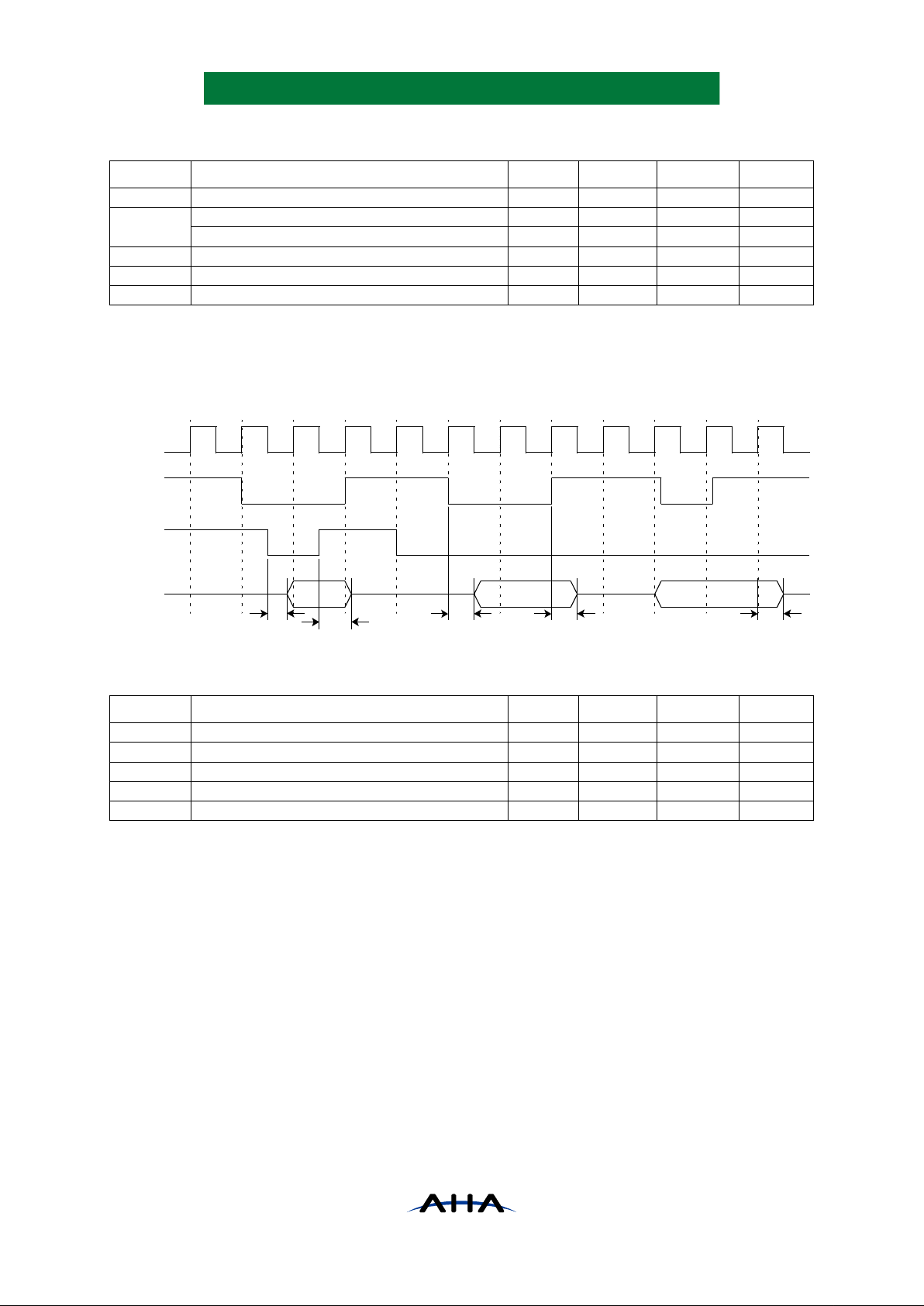
PS3410C-0600 Page 33 of 47
Advanced Hardware Architectures, Inc.
Table 7: Request vs. EOR Timing
Notes:
1) Production test condition is 50 pF. Delay is decreased 2 ns with 25 pF load guaranteed by design or
characterization.
Figure 23: Output Enable Timing
Table 8: Output Enable Timing Requirements
NUMBER PARAMETER MIN MAX UNITS NOTES
1 ACKN, SD to REQN DSC=0-15; ERC=0 20 ns 1
2
CLOCK to REQN DSC=0-3, 6-9; ERC=0 21 ns 1
CLOCK to REQN DSC=10-15; ERC=0 23 ns 1
3 CLOCK to REQN DSC=0-3, 6-15; ERC=1 18 ns 1
4 CLOCK to REQN DSC=4, 5; ERC=0 21 ns 1
5 CLOCK to REQN DSC=4, 5; ERC=1 18 ns 1
NUMBER PARAMETER MIN MAX UNITS NOTES
1 DRIVEN to D valid 15 ns
2 DRIVEN to D tristate 10 ns
3 Signal to D valid 15 ns
4 Signal to D tristate 10 ns
5 CLOCK to D tristate (DSC=100, 101) 15 ns
CLOCK
ACKN
DRIVEN
D
2
1 3 4 5
Page 40

Page 34 of 47 PS3410C-0600
Advanced Hardware Architectures, Inc.
Figure 24: Video Input Port Timing
Table 9: Video Input Port Timing Requirements
Figure 25: Video Output Port Timing
T a ble 10: Video Output Port Timing Requirements
Notes:
1) Production test condition is 50 pF. Delay is decreased 2 ns with 25 pF load guaranteed by design or
characterization.
NUMBER PARAMETER MIN MAX UNITS NOTES
1 VIREQN delay 16 ns
2 VIREQN hold 2 ns
3 VIACKN setup 8 ns
4 VIACKN hold 2 ns
5VID setup 8 ns
6 VID hold 2 ns
NUMBER PARAMETER MIN MAX UNITS NOTES
1 VOREQN delay 19 ns 1
2 VOREQN hold 4 ns
3 VOACKN setup 8 ns
4 VOACKN hold 3 ns
5 VOD delay 21 ns 1
6 VOD hold 3.7 ns
7 VOEORN hold 3.7 ns
8 VOEORN delay 21 ns 1
CLOCK
VIACKN
VID[7:0]
VIREQN
1
3
65
4
2
CLOCK
VOACKN
VOD[7:0]
VOREQN
1 2
43
6
VOEORN
5
7 8
Page 41

PS3410C-0600 Page 35 of 47
Advanced Hardware Architectures, Inc.
Figure 26: Microprocessor Interface Timing (PROCMODE[1]=0)
CLOCK
CSN
PA
RDYN
DIR
READ
11212
3 4
6
9
10
910
15
14
3
4
7
8
9 10
12 13
Valid
tristate
Valid
tristate
910
Valid
PD
DIR
PD
WRITE
234512
Page 42

Page 36 of 47 PS3410C-0600
Advanced Hardware Architectures, Inc.
Figure 27: Microprocessor Interface Timing (PROCMODE[1]=1)
Table 11: Microprocessor Interface Timing Requirements
NUMBER PARAMETER MIN MAX UNITS NOTES
1 PA setup time 10 ns
2 PA hold time 3 ns
3 CSN setup time 10 ns
4 CSN hold time 3 ns
6 CSN to valid RDYN 15 ns
7 RDYN valid delay 20 ns
8 RDYN drive disable 10 ns
9 DIR setup time 10 ns
10 DIR hold time 3 ns
12 PD valid delay 20 ns
13 PD drive disable 12 ns
14 PD setup time 10 ns
15 PD hold time 3 ns
16 CSN high to PD tristate 10 ns
17 CSN high to RDYN high 15 ns
CLOCK
CSN
PA
RDYN
DIR
READ
1
PD
DIR
PD
WRITE
123 5N4
Valid
Valid
A0
3
2
4
16
17
12
7
14
15
9
13
tristate
10
Page 43

PS3410C-0600 Page 37 of 47
Advanced Hardware Architectures, Inc.
Figure 28: Interrupt Timing
Table 12: Interrupt Timing Requirements
Figure 29: Clock Timing
Table 13: Clock Timing Requirements
Figure 30: Power On Reset Timing
Table 14: Power On Reset Timing Requirements
Notes:
1) RSTN signal can be asynchronous to the CLOCK signal. It is internally synchronized to the rising edge of
CLOCK.
NUMBER PARAMETER MIN MAX UNITS NOTES
1 INTRN delay time 15 ns
2 INTRN hold time 3 ns
NUMBER PARAMETER MIN MAX UNITS NOTES
1 CLOCK rise time 5 ns
2 CLOCK fall time 5 ns
3 CLOCK high time 15 ns
4 CLOCK low time 16 ns
5 CLOCK period 40 ns
NUMBER PARAMETER MIN MAX UNITS NOTES
1 RSTN low pulsewidth 10 clocks
2 RSTN setup to CLOCK rise 15 ns 1
3 RSTN hold time 2 ns 1
CLOCK
INTRN
1 2
CLK
1
34
5
2
2.0V
1.4V
0.8V
CLOCK
RSTN
2
3
1
Page 44

Page 38 of 47 PS3410C-0600
Advanced Hardware Architectures, Inc.
9.0 PACKAGE SPECIFICATIONS
Package is JEDEC MO-108
L
A
A
DETAIL A
A2
A1
E1
D1
P
P
D
B
E
117
118
119
120
3029282726
AHA3410C-025 PQC
91
92
93
94
(LCA)
(LCB)
Page 45

PS3410C-0600 Page 39 of 47
Advanced Hardware Architectures, Inc.
JEDEC Outline MO-108
10.0 ORDERING INFORMATION
10.1 AVAILABLE PARTS
10.2 PART NUMBERING
Device Number:
3410
Revision Letter:
C
Package Material Codes:
P Plastic
Package Ty pe Codes:
Q Quad Flat Pack
Test Specifications:
C Commercial 0°C to +70°C
PLASTIC QUAD FLAT PACK PACKAGE DIMENSIONS
(All dimensions are in mm)
SYMBOL
NUMBER OF PIN AND SPECIFICATION DIMENSION
120
SB
MIN NOM MAX
(LCA) 30
(LCB) 30
A 3.7 4.07
A1 0.25 0.33
A2 3.2 3.37 3.6
D 30.95 31.2 31.45
D1 27.99 28 28.12
E 30.95 31.2 31.45
E1 27.99 28 28.12
L 0.73 0.88 1.03
P0.8
B 0.3 0.35 0.4
PART NUMBER DESCRIPTION
AHA3410C-025 PQC
25 MBytes/sec Simultan eous Lossless Data Compression/
Decompression Coprocessor IC
AHA 3410 C- 025 P Q C
Manufacturer
Device
Number
Revision
Level
Speed
Designation
Package
Material
Package
Type
Test
Specification
Page 46

Page 40 of 47 PS3410C-0600
Advanced Hardware Architectures, Inc.
1 1.0 RELATED PUBLICATIONS
11.1 AHA TECHNICAL PUBLICATIONS
* Evaluation Software is also available for UNIX operating system, upon request.
11.2 OTHER TECHNICAL PUBLICATIONS
DOCUMENT # DESCRIPTION
PB3410C
AHA Product Brief – AHA3410C StarLite
TM
25 MBytes/sec Simultaneous
Lossless Da ta Compressi on/Decompression Coprocessor IC
PB3411
AHA Product Brief – AHA3411 StarLite
TM
33 MBytes/sec Simultaneous
Compressor/Decompressor IC
PB3422
AHA Product Brief – AHA3422 StarLite
TM
16 MBytes/sec Lossless
Decompressor IC
PB3431
AHA Product Brief – AHA3431 StarLite™ 40 MBytes/sec Simultaneous
Compressor/Decompressor IC, 3.3V
PS3411
AHA Product Specification – AHA3411 StarLite
TM
33 MBytes/sec Simultaneous
Compressor/Decompressor IC
PS3422
AHA Product Specification – AHA3422 StarLite
TM
16 MBytes/sec Lossless
Decompressor IC
PS3431
AHA Product Specificati on – AHA3431 S tarLite
TM
40 MBytes/sec Simultaneous
Compressor/Decompressor IC, 3.3V
ANDC12 AHA Application Note – AHA3410 StarLite
TM
Designer’s Guide
ANDC13 AHA Application Note – Compression Performance on Bitonal Images
ANDC14 AHA Application Note – StarLite
TM
Evaluation Software
ANDC15 AHA Application Note – ENCODEB2 Compression Algorithm Description
ANDC16
AHA Application Note – Designer’s Guide for StarLit e
TM
Family Products:
AHA3411, AHA3422 and AHA3431
ANDC17 AHA Application Note – StarLite
TM
Compression on Continuous Tone Images
GLGEN1 General Glossary of Terms
STARSW StarLite
TM
Evaluation Software (WindowsTM)
PCTP127
T. Summers, “Applying Compression/Decompression in High-Performance
Printers and Copiers”, Conference Proce eding: Th e 1995 Sil icon Valley Pers onal
Computer Design Conference and Exposition
T. Summers, “Compression Technologies in Printers”, A paper presentation at
Seybold Conference, 1995
DOCUMENT # DESCRIPTION
7th Edition, 1995 AMD’s Fusion29K® Catalog
6th Edition, 1995 Intel’s Solutions 960® Catalog
1996 Edition
Motorola’s 68K & ColdFIRE® Source Book: High Performance
Embedded Systems
Page 47
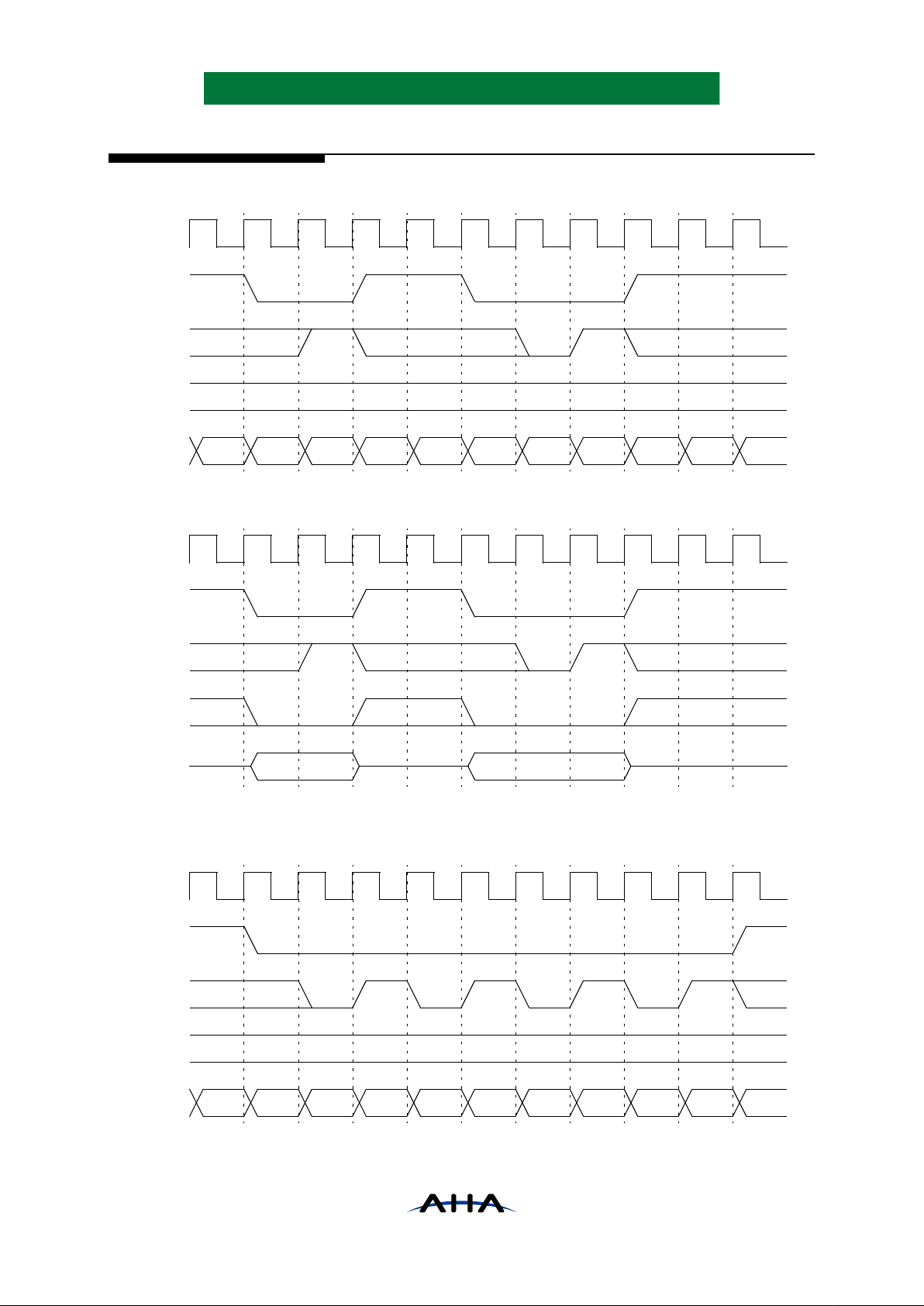
PS3410C-0600 Page 41 of 47
Advanced Hardware Architectures, Inc.
APPENDIX A: ADDITIONAL TIMING DIAGRAMS FOR DMA MODE TRANSFERS
Figure A1: DMA Mode Timing for Single Word Writes, Strobe Condition of DSC=000
Figure A2: DMA Mode Timing for Single Word Reads, Strobe Condition of DSC=000
Figure A3: DMA Mode Timing for Four Word Burst Write, One Wait State, Strobe Condition
of DSC=000
CLOCK
ACKN
SD
DRIVEN
D
D0 D1
CLOCK
ACKN
SD
DRIVEN
D
D1D0
CLOCK
ACKN
SD
DRIVEN
D
D0 D2D1 D3
Page 48

Page 42 of 47 PS3410C-0600
Advanced Hardware Architectures, Inc.
Figure A4: DMA Mode Timing for Four Word Burst Read, One Wait State, Strobe Condition
of DSC=000
Figure A5: DMA Mode Timing for Eight Word Burst Write, Zero Wait State, Strobe Condition
of DSC=000
Figure A6: DMA Mode Timing for Eight Word Burst Read, Zero Wait State, Strobe Condition
of DSC=000
CLOCK
ACKN
SD
DRIVEN
D
D1D0 D2 D3
CLOCK
ACKN
SD
DRIVEN
D
D0 D2D1 D3 D4 D5 D6 D7
CLOCK
ACKN
SD
DRIVEN
D
D0 D2D1 D3 D4 D5 D6 D7
Page 49

PS3410C-0600 Page 43 of 47
Advanced Hardware Architectures, Inc.
Figure A7: DMA Mode Timing for Single Word Writes, Strobe Condition ofDSC=010
Figure A8: DMA Mode Timing for Single Word Reads, Strobe Condition of DSC=010
Figure A9: DMA Mode Timing for Four Word Burst Write, One Wait State, Strobe Condition
of DSC=010
CLOCK
ACKN
SD
DRIVEN
D
D0 D1
CLOCK
ACKN
SD
DRIVEN
D
D1D0
CLOCK
ACKN
SD
DRIVEN
D
D0 D2D1 D3
Page 50

Page 44 of 47 PS3410C-0600
Advanced Hardware Architectures, Inc.
Figure A10: DMA Mode Timing for Four Word Burst Read, One Wait State, Strobe Condition
of DSC=010
Figure A11: DMA Mode Timing for Eight Word Burst Write, Zero Wait State, Strobe Condition
of DSC=010
Figure A12: DMA Mode Timing for Eight Word Burst Read, Zero Wait State, Strobe Condition
of DSC=010
CLOCK
ACKN
SD
DRIVEN
D
D1D0 D2 D3
CLOCK
ACKN
SD
DRIVEN
D
D0 D2D1 D3 D4 D5 D6 D7
CLOCK
ACKN
SD
DRIVEN
D
D2D1 D3 D4 D5 D6 D7D0
Page 51

PS3410C-0600 Page 45 of 47
Advanced Hardware Architectures, Inc.
Figure A13: DMA Mode Timing for Single Word Writes, Strobe Condition ofDSC=011
Figure A14: DMA Mode Timing for Single Word Reads, Strobe Condition of DSC=011
Figure A15: DMA Mode Timing for Four Word Burst Write, One Wait State, Strobe Condition
of DSC=011
CLOCK
ACKN
SD
DRIVEN
D
D0 D1
CLOCK
ACKN
SD
DRIVEN
D
D1D0
CLOCK
ACKN
SD
DRIVEN
D
D0 D2D1 D3
Page 52

Page 46 of 47 PS3410C-0600
Advanced Hardware Architectures, Inc.
Figure A16: DMA Mode Timing for Four Word Burst Read, One Wait State, Strobe Condition
of DSC=011
Figure A17: DMA Mode Timing for Eight Word Burst Write, Zero Wait State, Strobe Condition
of DSC=011
Figure A18: DMA Mode Timing for Eight Word Burst Read, Zero Wait State, Strobe Condition
of DSC=011
CLOCK
ACKN
SD
DRIVEN
D
D1D0 D2 D3
CLOCK
ACKN
SD
DRIVEN
D
D0 D2D1 D3 D4 D5 D6 D7
CLOCK
ACKN
SD
DRIVEN
D
D2D1 D3 D4 D5 D6 D7D0
Page 53

PS3410C-0600 Page 47 of 47
Advanced Hardware Architectures, Inc.
Figure A19: DMA Mode Timing for Single Word Writes, Strobe Condition ofDSC=111
Figure A20: DMA Mode Timing for Single Word Reads, Strobe Condition ofDSC=111
CLOCK
ACKN
SD
DRIVEN
D
D0 D1 D2
CLOCK
ACKN
SD
DRIVEN
D
D1D0 D2
 Loading...