

Advanced Hardware Architectures AHA3210B-020PQC Datasheet

PS3210B-1299
The Data Coding Leader
Advanced Hardware
Architectures
TM
Advanced Hardware
Architectures, Inc.
2365 NE Hopkins Court
Pullman, WA 99163-5601
509.334.1000
Fax: 509.334.9000
e-mail: sales@aha.com
http://www.aha.com
Product Specification
AHA3210B
10 MBytes/sec DCLZ
Data Compression Coprocessor IC

Advanced Hardware Architectures, Inc.
PS3210B-1299 i
Table of Contents
1.0 Introduction . . . . . . . . . . . . . . . . . . . . . . . . . . . . . . . . . . . . . . . . . . . . . . . . . . . . . . . . . . . . . . . . . . . . . . . . . . . . .1
1.1 Features . . . . . . . . . . . . . . . . . . . . . . . . . . . . . . . . . . . . . . . . . . . . . . . . . . . . . . . . . . . . . . . . . . . . . . . . . . . .1
1.2 Applications. . . . . . . . . . . . . . . . . . . . . . . . . . . . . . . . . . . . . . . . . . . . . . . . . . . . . . . . . . . . . . . . . . . . . . . . . .1
1.3 Functional Overview . . . . . . . . . . . . . . . . . . . . . . . . . . . . . . . . . . . . . . . . . . . . . . . . . . . . . . . . . . . . . . . . . . .1
2.0 Modes of Operation. . . . . . . . . . . . . . . . . . . . . . . . . . . . . . . . . . . . . . . . . . . . . . . . . . . . . . . . . . . . . . . . . . . . . . .2
2.1 Port A and B Port Data Bus Configuration . . . . . . . . . . . . . . . . . . . . . . . . . . . . . . . . . . . . . . . . . . . . . . . . . .2
2.1.1 Dual Data Bus Mode: In-Line Application. . . . . . . . . . . . . . . . . . . . . . . . . . . . . . . . . . . . . . . . . . . . .3
2.1.2 Single Data Bus Mode: Look-Aside Application. . . . . . . . . . . . . . . . . . . . . . . . . . . . . . . . . . . . . . . .3
2.1.3 Port A Peripheral Chip Interface. . . . . . . . . . . . . . . . . . . . . . . . . . . . . . . . . . . . . . . . . . . . . . . . . . . .4
2.2 Data Processing Modes . . . . . . . . . . . . . . . . . . . . . . . . . . . . . . . . . . . . . . . . . . . . . . . . . . . . . . . . . . . . . . . .4
2.2.1 Compression Mode . . . . . . . . . . . . . . . . . . . . . . . . . . . . . . . . . . . . . . . . . . . . . . . . . . . . . . . . . . . . .4
2.2.2 Compression Flush Mode. . . . . . . . . . . . . . . . . . . . . . . . . . . . . . . . . . . . . . . . . . . . . . . . . . . . . . . . .5
2.2.3 Decompression Mode. . . . . . . . . . . . . . . . . . . . . . . . . . . . . . . . . . . . . . . . . . . . . . . . . . . . . . . . . . . .7
2.2.4 Decompression Output Disabled Mode . . . . . . . . . . . . . . . . . . . . . . . . . . . . . . . . . . . . . . . . . . . . . .8
2.2.5 Pass Through A to B Mode . . . . . . . . . . . . . . . . . . . . . . . . . . . . . . . . . . . . . . . . . . . . . . . . . . . . . . .9
2.2.6 Pass Through B to A Mode . . . . . . . . . . . . . . . . . . . . . . . . . . . . . . . . . . . . . . . . . . . . . . . . . . . . . .10
3.0 Register Description . . . . . . . . . . . . . . . . . . . . . . . . . . . . . . . . . . . . . . . . . . . . . . . . . . . . . . . . . . . . . . . . . . . . .11
3.1 DCLZ Control: Address 00 Hex - Read/Write . . . . . . . . . . . . . . . . . . . . . . . . . . . . . . . . . . . . . . . . . . . . . . .12
3.2 DCLZ Status: Address 01 Hex - Read Only . . . . . . . . . . . . . . . . . . . . . . . . . . . . . . . . . . . . . . . . . . . . . . . .13
3.3 Comp Ratio Optimization: Address 02 Hex - Read/Write . . . . . . . . . . . . . . . . . . . . . . . . . . . . . . . . . . . . . .14
3.4 DMA Configuration: Address 03 Hex - Read/Write. . . . . . . . . . . . . . . . . . . . . . . . . . . . . . . . . . . . . . . . . . .14
3.5 Port A Control 0: Address 04 Hex - Read/Write . . . . . . . . . . . . . . . . . . . . . . . . . . . . . . . . . . . . . . . . . . . . .15
3.6 Port A Control 1: Address 05 Hex - Read/Write . . . . . . . . . . . . . . . . . . . . . . . . . . . . . . . . . . . . . . . . . . . . .16
3.7 Port A Status: Address 06 Hex - Read Only . . . . . . . . . . . . . . . . . . . . . . . . . . . . . . . . . . . . . . . . . . . . . . . .17
3.8 Port A Byte Count: Address 07,08,09 Hex - Read/Write. . . . . . . . . . . . . . . . . . . . . . . . . . . . . . . . . . . . . . .18
3.9 Port B Control 0: Address 0A Hex - Read/Write . . . . . . . . . . . . . . . . . . . . . . . . . . . . . . . . . . . . . . . . . . . . .18
3.10 Port B ControL 1: Address 0B Hex - Read/Write. . . . . . . . . . . . . . . . . . . . . . . . . . . . . . . . . . . . . . . . . . . . .19
3.11 Port B Status: Address 0C Hex - Read Only. . . . . . . . . . . . . . . . . . . . . . . . . . . . . . . . . . . . . . . . . . . . . . . .20
3.12 Port B Byte Count: Address 0D,0E,0F Hex - Read/Write . . . . . . . . . . . . . . . . . . . . . . . . . . . . . . . . . . . . . .20
3.13 Port B Byte Comparator: Address 10,11,12 Hex - Read/Write . . . . . . . . . . . . . . . . . . . . . . . . . . . . . . . . . .21
3.14 Record Length: Address 13,14,15 Hex - Read/Write . . . . . . . . . . . . . . . . . . . . . . . . . . . . . . . . . . . . . . . . .2 1
3.15 Record Count: Address 16,17,18 Hex - Read/Write . . . . . . . . . . . . . . . . . . . . . . . . . . . . . . . . . . . . . . . . . .22
3.16 Interrupt Status: Address 19 Hex - Read Only . . . . . . . . . . . . . . . . . . . . . . . . . . . . . . . . . . . . . . . . . . . . . .22
3.17 Interrupt Clear: Address 19 Hex - Write Only . . . . . . . . . . . . . . . . . . . . . . . . . . . . . . . . . . . . . . . . . . . . . . .23
3.18 Interrupt Disable: Address 1A Hex - Read/Write. . . . . . . . . . . . . . . . . . . . . . . . . . . . . . . . . . . . . . . . . . . . .23
3.19 Identification: Address 1F Hex - Read Only . . . . . . . . . . . . . . . . . . . . . . . . . . . . . . . . . . . . . . . . . . . . . . . .23
4.0 Pin Description. . . . . . . . . . . . . . . . . . . . . . . . . . . . . . . . . . . . . . . . . . . . . . . . . . . . . . . . . . . . . . . . . . . . . . . . . .24
4.1 Processor Interface. . . . . . . . . . . . . . . . . . . . . . . . . . . . . . . . . . . . . . . . . . . . . . . . . . . . . . . . . . . . . . . . . . .24
4.2 Port A Interface . . . . . . . . . . . . . . . . . . . . . . . . . . . . . . . . . . . . . . . . . . . . . . . . . . . . . . . . . . . . . . . . . . . . . .26
4.3 Port B Interface . . . . . . . . . . . . . . . . . . . . . . . . . . . . . . . . . . . . . . . . . . . . . . . . . . . . . . . . . . . . . . . . . . . . . .27
5.0 Pinout . . . . . . . . . . . . . . . . . . . . . . . . . . . . . . . . . . . . . . . . . . . . . . . . . . . . . . . . . . . . . . . . . . . . . . . . . . . . . . . . .28
6.0 Electrical Specifications . . . . . . . . . . . . . . . . . . . . . . . . . . . . . . . . . . . . . . . . . . . . . . . . . . . . . . . . . . . . . . . . . .29
6.1 Absolute Maximum Ratings. . . . . . . . . . . . . . . . . . . . . . . . . . . . . . . . . . . . . . . . . . . . . . . . . . . . . . . . . . . . .29
6.2 Recommended Operating Conditions. . . . . . . . . . . . . . . . . . . . . . . . . . . . . . . . . . . . . . . . . . . . . . . . . . . . .29
6.2.1 DC Specifications. . . . . . . . . . . . . . . . . . . . . . . . . . . . . . . . . . . . . . . . . . . . . . . . . . . . . . . . . . . . . .29
6.2.2 AC Specifications. . . . . . . . . . . . . . . . . . . . . . . . . . . . . . . . . . . . . . . . . . . . . . . . . . . . . . . . . . . . . .29
6.2.3 Pin Capacitance. . . . . . . . . . . . . . . . . . . . . . . . . . . . . . . . . . . . . . . . . . . . . . . . . . . . . . . . . . . . . . .30
7.0 Timing Specifications . . . . . . . . . . . . . . . . . . . . . . . . . . . . . . . . . . . . . . . . . . . . . . . . . . . . . . . . . . . . . . . . . . . .31

Advanced Hardware Architectures, Inc.
ii PS3210B-1299
8.0 Packaging. . . . . . . . . . . . . . . . . . . . . . . . . . . . . . . . . . . . . . . . . . . . . . . . . . . . . . . . . . . . . . . . . . . . . . . . . . . . . .44
9.0 Ordering Information. . . . . . . . . . . . . . . . . . . . . . . . . . . . . . . . . . . . . . . . . . . . . . . . . . . . . . . . . . . . . . . . . . . . .45
9.1 Available Parts. . . . . . . . . . . . . . . . . . . . . . . . . . . . . . . . . . . . . . . . . . . . . . . . . . . . . . . . . . . . . . . . . . . . . . .45
9.2 Part Numbering. . . . . . . . . . . . . . . . . . . . . . . . . . . . . . . . . . . . . . . . . . . . . . . . . . . . . . . . . . . . . . . . . . . . . .45
10.0 AHA Related Technical Publications. . . . . . . . . . . . . . . . . . . . . . . . . . . . . . . . . . . . . . . . . . . . . . . . . . . . . . . .45

Advanced Hardware Architectures, Inc.
PS3210B-1299 iii
Figures
Figure 1: Functional Block Diagram . . . . . . . . . . . . . . . . . . . . . . . . . . . . . . . . . . . . . . . . . . . . . . . . . . . . . . . . . . . . . .2
Figure 2: Dual Data Bus Mode . . . . . . . . . . . . . . . . . . . . . . . . . . . . . . . . . . . . . . . . . . . . . . . . . . . . . . . . . . . . . . . . . .3
Figure 3: Single Data Bus Mode. . . . . . . . . . . . . . . . . . . . . . . . . . . . . . . . . . . . . . . . . . . . . . . . . . . . . . . . . . . . . . . . .3
Figure 4: Port A Peripheral Chip Interface . . . . . . . . . . . . . . . . . . . . . . . . . . . . . . . . . . . . . . . . . . . . . . . . . . . . . . . . .4
Figure 5: Compression Mode . . . . . . . . . . . . . . . . . . . . . . . . . . . . . . . . . . . . . . . . . . . . . . . . . . . . . . . . . . . . . . . . . . .5
Figure 6: Compression Flush Mode . . . . . . . . . . . . . . . . . . . . . . . . . . . . . . . . . . . . . . . . . . . . . . . . . . . . . . . . . . . . . .6
Figure 7: Decompression Mode . . . . . . . . . . . . . . . . . . . . . . . . . . . . . . . . . . . . . . . . . . . . . . . . . . . . . . . . . . . . . . . . .7
Figure 8: Decompression Output Disabled Mode. . . . . . . . . . . . . . . . . . . . . . . . . . . . . . . . . . . . . . . . . . . . . . . . . . . .8
Figure 9: Pass Through A to B Mode . . . . . . . . . . . . . . . . . . . . . . . . . . . . . . . . . . . . . . . . . . . . . . . . . . . . . . . . . . . . .9
Figure 10: Pass Through B to A Mode . . . . . . . . . . . . . . . . . . . . . . . . . . . . . . . . . . . . . . . . . . . . . . . . . . . . . . . . . . . .10
Figure 11: Pinout Diagram . . . . . . . . . . . . . . . . . . . . . . . . . . . . . . . . . . . . . . . . . . . . . . . . . . . . . . . . . . . . . . . . . . . . .28
Figure 12: Dynamic Current - Idd vs. Compression Ratio. . . . . . . . . . . . . . . . . . . . . . . . . . . . . . . . . . . . . . . . . . . . . .30
Figure 13: Clock Timing . . . . . . . . . . . . . . . . . . . . . . . . . . . . . . . . . . . . . . . . . . . . . . . . . . . . . . . . . . . . . . . . . . . . . . .31
Figure 14: Reset Timing - Power Up. . . . . . . . . . . . . . . . . . . . . . . . . . . . . . . . . . . . . . . . . . . . . . . . . . . . . . . . . . . . . .31
Figure 15: Reset Timing . . . . . . . . . . . . . . . . . . . . . . . . . . . . . . . . . . . . . . . . . . . . . . . . . . . . . . . . . . . . . . . . . . . . . . .31
Figure 16: Processor Read Cycle - DSN, RWN Controlled. . . . . . . . . . . . . . . . . . . . . . . . . . . . . . . . . . . . . . . . . . . . .32
Figure 17: Processor Write Cycle - DSN, RWN Controlled. . . . . . . . . . . . . . . . . . . . . . . . . . . . . . . . . . . . . . . . . . . . .33
Figure 18: Processor Read Cycle - IORDN Controlled. . . . . . . . . . . . . . . . . . . . . . . . . . . . . . . . . . . . . . . . . . . . . . . .34
Figure 19: Processor Write Cycle - IOWRN Controlled. . . . . . . . . . . . . . . . . . . . . . . . . . . . . . . . . . . . . . . . . . . . . . . .35
Figure 20: Processor Read Cycle from Port A Peripheral - DSN, RWN Controlled . . . . . . . . . . . . . . . . . . . . . . . . . .36
Figure 21: Processor Write Cycle to Port A Peripheral - DSN, RWN Controlled . . . . . . . . . . . . . . . . . . . . . . . . . . . .37
Figure 22: Processor Read Cycle from Port A Peripheral - IORDN Controlled. . . . . . . . . . . . . . . . . . . . . . . . . . . . . .38
Figure 23: Processor Write Cycle to Port A Peripheral - IOWRN Controlled . . . . . . . . . . . . . . . . . . . . . . . . . . . . . . .39
Figure 24: DMA Slave Transfer Timing for Data Into Port A,B . . . . . . . . . . . . . . . . . . . . . . . . . . . . . . . . . . . . . . . . . .40
Figure 25: DMA Slave Transfer Timing for Data Out of Port A,B . . . . . . . . . . . . . . . . . . . . . . . . . . . . . . . . . . . . . . . .41
Figure 26: DMA Master Transfer Timing for Data Into Port A,B . . . . . . . . . . . . . . . . . . . . . . . . . . . . . . . . . . . . . . . . .42
Figure 27: DMA Master Transfer Timing for Data Out of Port A,B . . . . . . . . . . . . . . . . . . . . . . . . . . . . . . . . . . . . . . .43
Figure 28: AHA3210B Package Specifications. . . . . . . . . . . . . . . . . . . . . . . . . . . . . . . . . . . . . . . . . . . . . . . . . . . . . .44

Advanced Hardware Architectures, Inc.
iv PS3210B-1299
Tables
Table 1: Data Bus Modes . . . . . . . . . . . . . . . . . . . . . . . . . . . . . . . . . . . . . . . . . . . . . . . . . . . . . . . . . . . . . . . . . . . . .3
Table 2: Register Address Map. . . . . . . . . . . . . . . . . . . . . . . . . . . . . . . . . . . . . . . . . . . . . . . . . . . . . . . . . . . . . . . .11
Table 3: DCLZ Mode Bit Decode. . . . . . . . . . . . . . . . . . . . . . . . . . . . . . . . . . . . . . . . . . . . . . . . . . . . . . . . . . . . . . .12
Table 4: Supported Modes for DCLZ Control Register Bits. . . . . . . . . . . . . . . . . . . . . . . . . . . . . . . . . . . . . . . . . . .13
Table 5: DATA BUS MODE Bit Decode. . . . . . . . . . . . . . . . . . . . . . . . . . . . . . . . . . . . . . . . . . . . . . . . . . . . . . . . . .15
Table 6: Port A DMA Bus Master/Slave Pin Configuration . . . . . . . . . . . . . . . . . . . . . . . . . . . . . . . . . . . . . . . . . . .15
Table 7: Port B DMA Bus Master/Slave Pin Configuration . . . . . . . . . . . . . . . . . . . . . . . . . . . . . . . . . . . . . . . . . . .15
Table 8: Clock Timing Specification. . . . . . . . . . . . . . . . . . . . . . . . . . . . . . . . . . . . . . . . . . . . . . . . . . . . . . . . . . . . .31
Table 9: Reset Timing Specifications. . . . . . . . . . . . . . . . . . . . . . . . . . . . . . . . . . . . . . . . . . . . . . . . . . . . . . . . . . . .31
Table 10: Processor Read Cycle Timings - DSN, RWN Controlled. . . . . . . . . . . . . . . . . . . . . . . . . . . . . . . . . . . . . .32
Table 11: Processor Write Cycle Timings - DSN, RWN Controlled. . . . . . . . . . . . . . . . . . . . . . . . . . . . . . . . . . . . . .33
Table 12: Processor Read Cycle Timings - IORDN Controlled . . . . . . . . . . . . . . . . . . . . . . . . . . . . . . . . . . . . . . . . .34
Table 13: Processor Write Cycle Timings - IOWRN Controlled . . . . . . . . . . . . . . . . . . . . . . . . . . . . . . . . . . . . . . . . .35
Table 14: Processor Read Cycle Timings from Port A Peripheral - DSN, RWN Controlled . . . . . . . . . . . . . . . . . . .36
Table 15: Processor Write Cycle to Port A Peripheral Timings - DSN, RWN Controlled. . . . . . . . . . . . . . . . . . . . . .37
Table 16: Processor Read Cycle from Port A Peripheral Timings - IORDN Controlled . . . . . . . . . . . . . . . . . . . . . . .38
Table 17: Processor Write Cycle to Port A Peripheral Timings - IOWRN Controlled. . . . . . . . . . . . . . . . . . . . . . . . .39
Table 18: DMA Slave Transfer Timing for Data Into Port A,B . . . . . . . . . . . . . . . . . . . . . . . . . . . . . . . . . . . . . . . . . .40
Table 19: DMA Slave Transfer Timing for Data Out of Port A,B . . . . . . . . . . . . . . . . . . . . . . . . . . . . . . . . . . . . . . . .41
Table 20: DMA Master Transfer Timing for Data Into Port A,B . . . . . . . . . . . . . . . . . . . . . . . . . . . . . . . . . . . . . . . . .42
Table 21: DMA Master Transfer Timing for Data Out of Port A,B . . . . . . . . . . . . . . . . . . . . . . . . . . . . . . . . . . . . . . .43

PS3210B-1299 Page 1 of 45
Advanced Hardware Architectures, Inc.
1.0 INTRODUCTION
The AHA3210B is a single-chip CMOS
lossless compression and decompression int egrated
circuit under development implementing the
industry standard Data Compression Lempel Ziv
(DCLZ) adaptive compression algorithm. The
device processes data in compression,
decompression or pass-through modes. The
AHA3210B is based on the earlier 10 MBytes/sec
introduction, AHA3210. It maintains the same
pinout, performance, flexibility and I/O interface as
AHA3210.
Content Addressable Memor y within the DCLZ
engine eliminates external SRAMs typically
required for dictionary storage in a compression
system. Other supporting system features include
two 24-bit counters, automatic multiple-record
transfer, compression ratio optimization and DCLZ
error detection logic.
The DCLZ algorithm is approved by several
standards organi zations including QIC, DA T , ANSI,
ISO and ECMA. DCLZ has been accepted by
Hewlett-Packard and other system companies
worldwide as their standard of choice in their tape
storage peripherals. The algorithm exhibits an
average compression ratio of 2 to 1 over typical
computer data.
This specification contains a functional
overview, operation modes, register descriptions,
DC and AC Electrical characteristics, ordering
information and Related Technical Publications. It
is intended for hardware and software engineers
designing a compress ion system u sing AHA3210B.
AHA designs and develops lossless
compression, forward error correction and data
storage formatter/controller ICs. Technical
publications are available upon request from us or
our sales representatives/agents worldwide.
1.1 FEATURES
PERFORMANCE:
• 10 MBytes/sec data compressi on, decompr ession
or pass-through rate with a 20 MHz clock
• 2 to 1 average compression ratio
• High compression of small records
• Automatic multiple-record transfers without
microprocessor intervention
• Dynamic compression ratio monitoring
• Error checking in decompression mode
reportable via an interrupt
FLEXIBILITY:
• In-Line and Look-Aside architectures supported
• Polled or interrupt driven I/O
• Two independent DMA ports programmable for
8 or 16-bit t ransfers; mast er or slave mode
SYSTEM INTERFACE:
• Single chip data compression solution
• No SRAM required
• Programmable interrupts
• Interfaces directly with AHA’s tape format
controller, AHA5140, and industry standard
SCSI controllers
OTHERS:
• Open standard DCLZ adaptive lossless
compression algorithm
• Standards include: QIC DDS/DAT, ANSI, ISO
and ECMA
• Low power stand-by operation
• EIAJ-standard 100 pin plastic quad flat package
• Software emulation of the algorithm available
1.2 APPLICATIONS
• DDS-DAT, QIC, 8mm or DLT tape drives
• High performance laser printers
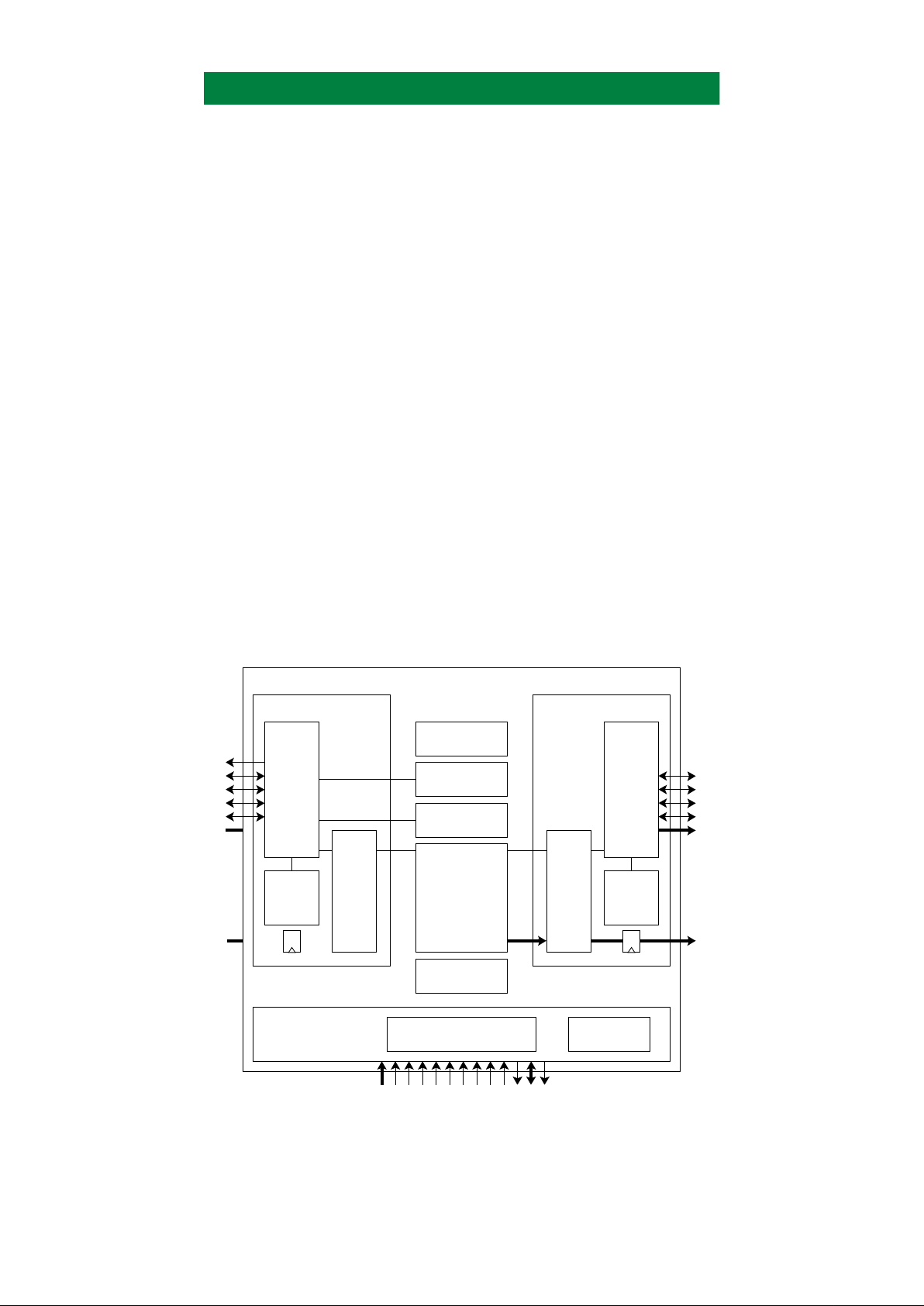
1.3 FUNCTIONAL OVERVIEW
The AHA3210B Data Compression
Coprocessor IC is a high performance, single chip
data compression solution, for use in tape drives,
disk drives and embedded controller applications.
The processor interface is us ed to t ran sf er da ta
to the registers inside the chip. The PROCMODE
strapping pin selects between a Motorola and an
Intel style processor interface.
The DCLZ Engine implements the DCLZ
lossless data compression algorithm. It contains a
compressor, which inputs uncompres sed data from
the Port A interface, compresses it, and sends the
compressed codes to the Port B interface. The
DCLZ Engine also contains a de compressor , whic h
inputs compressed co des f rom the Port B interfa ce,
decompresses it, and sends the uncompressed data
to the Port A interfac e. The Recor d Lengt h regis ter
and Record Count register al low uncompressed data
to be partitioned into fixed sized blocks, and then
compressed and decompressed automatically.
Page 2 of 45 PS3210B-1299
Advanced Hardware Architectures, Inc.
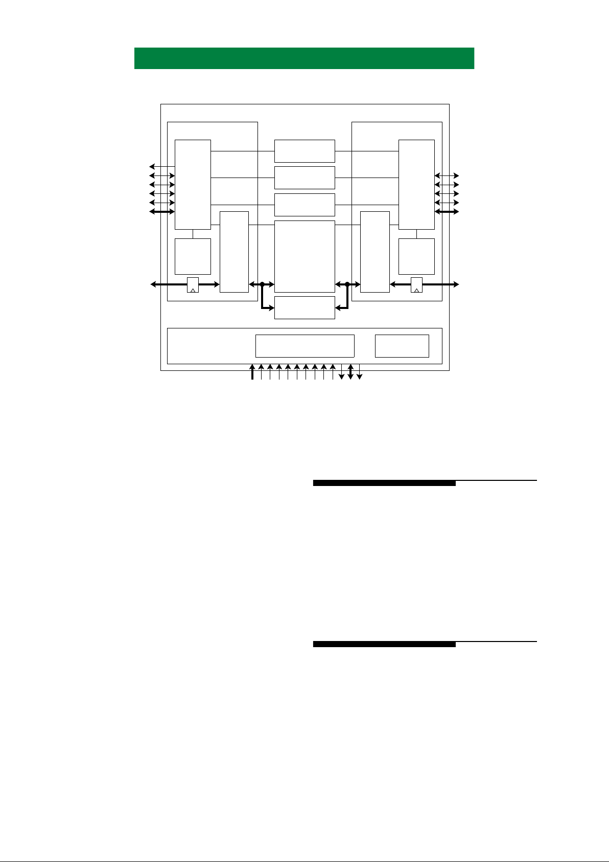
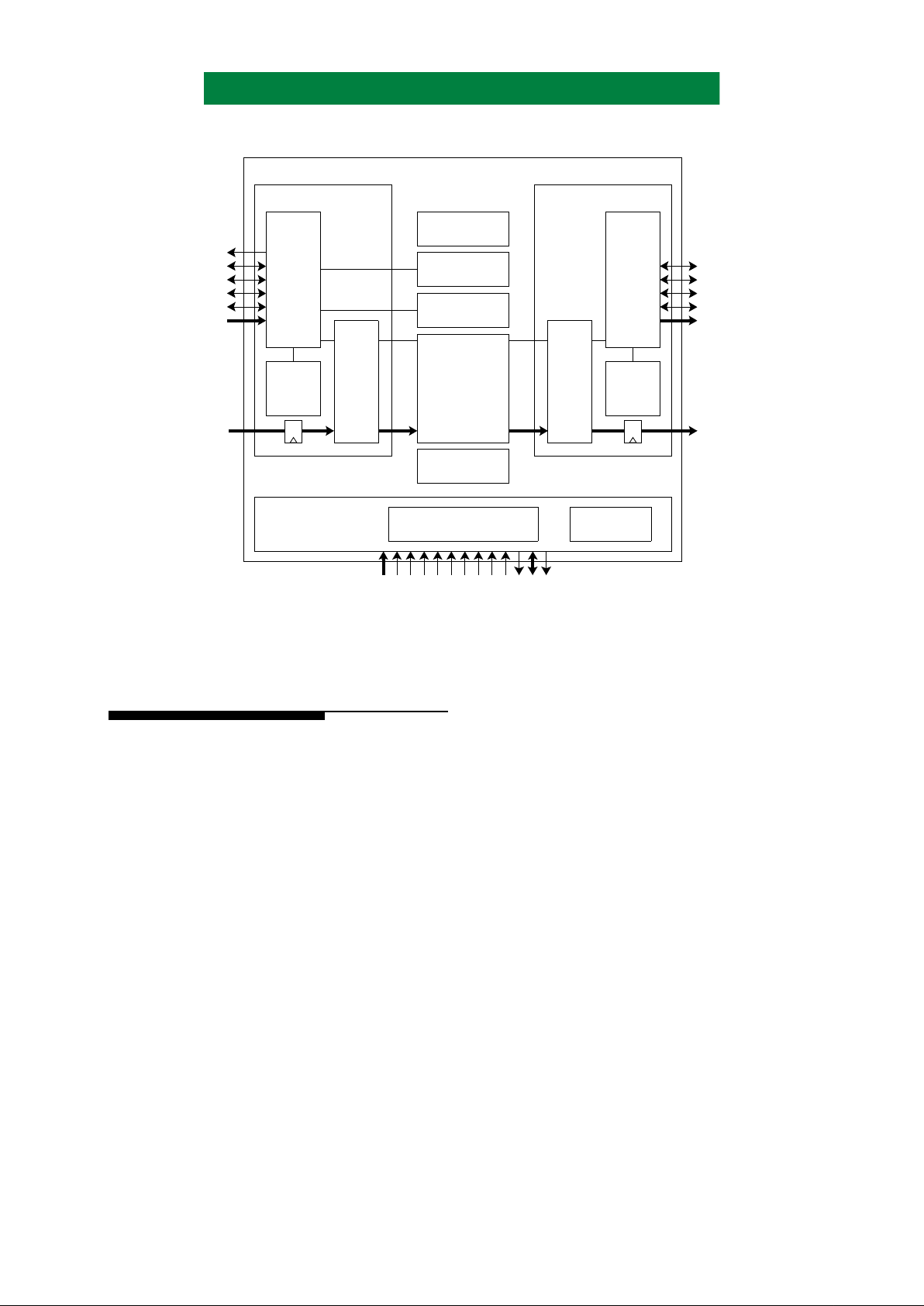
Figure 1: Functional Block Diagram
The Pass Through Controller bloc k allows data
to be transferred bet ween Port A and Port B without
being compressed or decompressed.
Port A and Port B are two independent DMA
interfaces. For compression and decompre ssi on
operations, Port A transf ers uncompressed data and
Port B transfers compre ssed cod es. Each p ort has a
byte counter , which counts the number of bytes that
are transferred through the port. The configuration
of the DMA interface on each po rt is programmable.
These functions incl ude DMA master or slave, eight
or sixteen bit t ransfers, and contr ol pin enabling and
polarity . The Port B Byte Count register has a Port B
Byte Comparator register, allowing the chip to
interrupt after a programmed amount of data has
been transferred on the Port B data bus, DB[15:0].
Register accesses to a peripheral chip connected to
Port A are also supported.
2.0 MODES OF OPERATION
There are two classes of the modes of operatio n
for this chip. The first class is determined by the
Port A and Port B DMA data bus configurations.
Port A and Port B can be dual independent data
buses, or Port A and Port B can be connected to
create a single data bus. The second class is
determined by the method data is processed through
the chip in compression, decompression or pass
through modes.
2.1 PORT A AND B PORT DATA BUS
CONFIGURATION
Port A and Port B data bus configuration is
controlled by the DATA BUS MODE[2:0] bits in
the DMA Configuration regi ster . These bits contro l
the single and dual data bus modes, as well as Port
A and Port B being the DMA bus master or slave
(see Table 1).
PORT A
BYTE
COUNTER
PORT B
BYTE
COUNTER
PORT A
DMA
STATE
MACHINE
PORT A
FIFO
PORT B
DMA
STATE
MACHINE
PORT B
FIFO
SINGLE DATA
BUS ARBITER
RECORD COUNT
REGISTER
RECORD LENGTH
REGISTER
PROCESSOR INTERFACE
STATE MACHINE
PASS THROUGH
CONTROLLER
INTERRUPT
LOGIC
PROCESSOR
INTERFACE
DCLZ
ENGINE
PORT A INTERFACE PORT B INTERFACE
ACSN
DREQA
DACKA
AOE
AWE
DAPTY[1:0]
DA[15:0]
A[4:0]
PORTACSN
CSN
RWN/IOWRN
DSN/IORDN
PROCMODE
TRISTATEN
TEST
RESTN
CLK
DTACKN/READY
D[7:0]
INTN/INT
DREQB
DACKB
BOE
BWE
DBPTY[1:0]
DB[15:0]
(8 Bytes) (8 Bytes)
AHA3210B Compression Chip
PS3210B-1299 Page 3 of 45
Advanced Hardware Architectures, Inc.
Table 1: Data Bus Modes
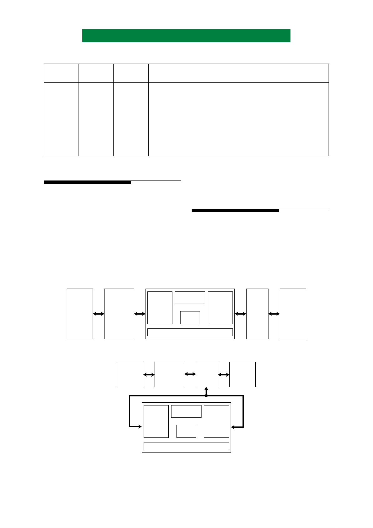
2.1.1 DUAL DATA BUS MODE: IN-LINE
APPLICATION
In dual data bus mode, Port A and Port B
transfer data on unique, independent data buses.
This is used for in-line applications, whe n data is
transferred from th e host interface, t hrough the data
compression coprocessor, and into the system
buffer (see Figure 2).
In dual data bus mode, the data rate during
compression is sustained at 10 MB/sec, except
when the compression ratio is less than 1 (which
occurs briefly when a compression dictionary is
first being built, or when data is actually
expanding). The data rate during decompression,
pass through A to B, a nd pass through B to A modes
is sustained at 10 MBytes/sec (see Figure 3).
2.1.2 SINGLE DATA BUS MODE: LOOK-ASIDE
APPLICATION
In single data bus mode, Port A and Port B
transfer data on a common data bus. This
connection is made external to the chip, on the PC
board. This is used in a look aside application, when
the data compression coproc essor transfers data into
and out of the system buffer.
Figure 2: Dual Data Bus Mode
Figure 3: Single Data Bus Mode
DATA BUS
MODE[2]
DA TA BUS
MODE[1]
DATA BUS
MODE[0]
FUNCTION
0 0 0 Dual data bus: Port B slave, Port A slave
0 0 1 Dual data bus: Port B slave, Port A master
0 1 0 Dual data bus: Port B master, Port A slave
0 1 1 Dual data bus: Port B master, Port A master
1 0 0 Dual data bus: Port B slave, Port A slave with peripheral access
101Reserved
1 1 0 Dual data bus: Port B master, Port A slave with peripheral access
1 1 1 Single data bus: Port B master, Port A master
HOST
INTERFACE
BUS
INTERFACE
PROCESSOR INTERFACE
SYSTEM
TAPE
DRIVE
BUS CONTROLLER
BUFFER
INTERFACE
PORT A
INTERFACE
SINGLE DATA
BUS ARBITER
DCLZ
ENGINE
PORT B
INTERFACE
HOST
INTERFACE
BUS
INTERFACE
PROCESSOR INTERFACE
SYSTEM
TAPE
DRIVE
BUS CONTROLLER
BUFFER
INTERFACE
PORT A
INTERFACE
SINGLE DATA
BUS ARBITER
DCLZ
ENGINE
PORT B
INTERFACE
Page 4 of 45 PS3210B-1299
Advanced Hardware Architectures, Inc.
2.1.3 PORT A PERIPHERAL CHIP INTERFACE
A peripheral chip can be connected to Port A,
and have its registers accessed through the
processor interface of the data compression chip
(see Figure 4). This is used in in-line applications,
for peripheral chips with a common DMA and
processor data bus (such as the NCR 53C90A/B and
the NCR 53C94/5/6 SCSI controllers).
It is the firm ware’s responsib ility to ensure
accesses to the peripheral chip’s registers do not
occur while DMA transfers ar e occurring on Port A.
This mode is only s upported when Port A is a DMA
slave, in dual data bus mode.
2.2 DATA PROCESSING MODES
The data processing modes a re controlled by the
DCLZ MODE[2:0] bits in the DCLZ Control
register.
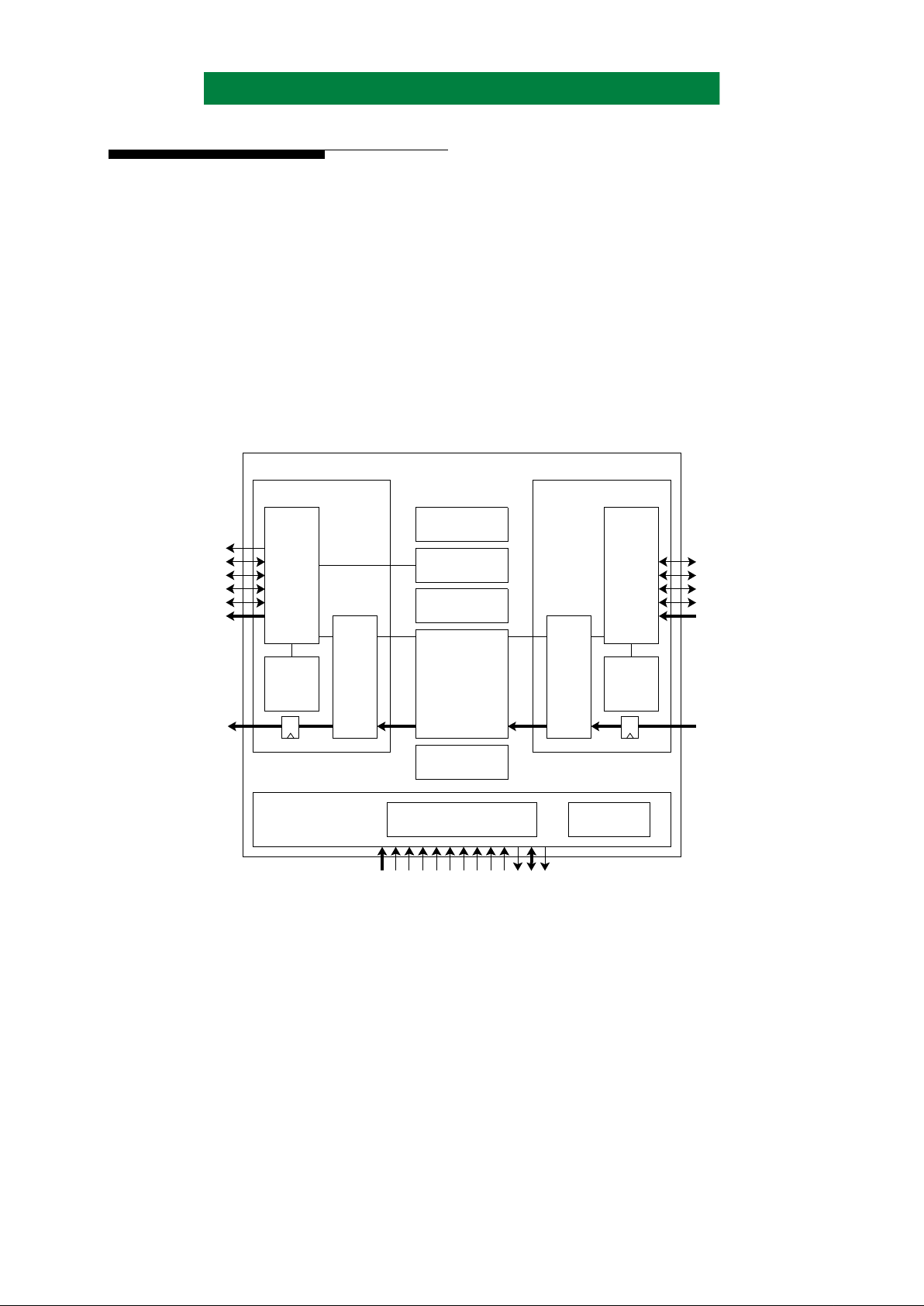
2.2.1 COMPRESSION MODE
During compression mode, uncompres sed data
flows into Port A. It is then comp ressed by the
DCLZ engine. The resulting compressed data is
then transferred out of Port B (see Figure 5).
The uncompressed data i s partitioned into fixed
sized recor ds. The size is stored in the Record
Length register inside the chip. After a record has
been compressed, an end of record codeword is
inserted into the compres sed data. The end of record
codewords are then used during decompression, to
control data flow.
Multiple records can be compressed without
processor intervention. The Record Count register
inside the chip stores the number of records to
compress. A compression sequence has been
completed after the last byte of the last record has
been compressed and transfer red out of Port B. This
event sets the Port B End of Transfer interrupt.
Compression ratio is defined as the number of
uncompressed bytes divided by the number of
compressed bytes. The Port A Byte Counter co unts
the number of uncompressed bytes. The Por t B Byte
Counter counts the number of compressed bytes.
The compression ratio can also be automatically
controlled, by programming the Comp Ratio
Optimization register.
The following sequence is used to p rog ram the
chip to compress multiple, fixed size records:
- Program Record Length register
- Program Record Count register
- Program Interrupt Disable register
- Enable PORT B END OF TRANSFER Interrupt
- Program Comp Ratio Optimization register
- Program DCLZ Control register
DCLZ MODE[2:0] Compression
COMP RATIO OPT ENABLE 1
RESET DICT AFTER EOR 0
RESET DICT 0
PAUSE AFTER EOR 0
PAUSE 0
- The PORT B END OF TRANSFER interrupt signals
compression completed
Figure 4: Port A Peripheral Chip Interface
PROCESSOR INTERFACE
DCLZ
ENGINE
PORT B
CS/
DREQ
DACK/
DBWR/
RD/
DBP[1:0]
DB[15:0]
DREQB
DACKB
BOE
BWE
DBPTY[1:0]
DB[15:0]
INTERFACE
ACSN
DREQA
DACKA
AOE
AWE
DAPTY[1:0]
DA[15:0]
WR/
A[3:0]
PORT A
INTERFACE
PERIPHERAL
A[4:0]
PORTACSN
CSN
RWN/IOWRN
DSN/IORDN
PROCMODE
TRISTATEN
TEST
RESETN
CLK
DTACKN/READY
D[7:0]
INTN/INT
CHIP
AHA3210B Compression Chip
PS3210B-1299 Page 5 of 45
Advanced Hardware Architectures, Inc.
Figure 5: Compression Mode
2.2.2 COMPRESSION FLUSH MODE
Normal compression operat ions complete when
the Record Length register and the Record Count
register both decrement to zero. All data in the chip
is then compressed, and transferred out of Port B.
There is no data in the chip, and the chip is said to be
flushed (see Figure 6).
Consider the scenario when a compression
operation is require d to comple te premat urel y (i.e.,
before the Record Length register and the Record
Count register have both decremented to zero). In
this scenario, Port A DMA i s inactive, because there
is no more uncompressed data to transfer into the
chip. Due to the DCLZ data compression algor ithm,
there may be partially compr essed data in the DCLZ
engine at this ti me.
Compression flush mode is used to complete
the compression operation , transfer all compr essed
data out of Port B, and get the chi p into t he flus hed
state. Note that the compression flush operation
inserts an end of recor d code word at the appropriate
location, near the end of the compressed data
stream.
The chip should only be programmed into
compression flus h m od e wh en the Port A Inter fa ce
is empty (i.e., when the Port Inte rface Byte Count in
the Port A Status register is zero) and the DCLZ
engine contains data (i.e., when the DCLZ Engine
Flushed bit in the DCLZ S tatus r egister is zero) and
the DCLZ Engine is not already in the process of
flushing (i.e., The DCLZ EOR COUNT bit in the
DCLZ Status register is zero).
PORT A
BYTE
COUNTER
PORT B
BYTE
COUNTER
PORT A
DMA
STATE
MACHINE
PORT A
FIFO
PORT B
DMA
STATE
MACHINE
PORT B
FIFO
SINGLE DATA
BUS ARBITER
RECORD COUNT
REGISTER
RECORD LENGTH
REGISTER
PROCESSOR INTERFACE
STATE MACHINE
PASS THROUGH
CONTROLLER
INTERRUPT
LOGIC
PROCESSOR
INTERFACE
DCLZ
ENGINE
PORT A INTERFACE PORT B INTERFACE
ACSN
DREQA
DACKA
AOE
AWE
DAPTY[1:0]
DA[15:0]
A[4:0]
PORTACSN
CSN
RWN/IOWRN
DSN/IORDN
PROCMODE
TRISTATEN
TEST
RESTN
CLK
DTACKN/READY
D[7:0]
INTN/INT
DREQB
DACKB
BOE
BWE
DBPTY[1:0]
DB[15:0]
(8 Bytes) (8 Bytes)
AHA3210B Compression Chip
Page 6 of 45 PS3210B-1299
Advanced Hardware Architectures, Inc.
The following sequence is use d to prog ram the
chip for Compression Flush mode for the scenario
described above:
- Program DCLZ Control register
DCLZ MODE[2:0] Compression
COMP RATIO OPT ENABLE 1
RESET DICT AFTER EOR 0
RESET DICT 0
PAUSE AFTER EOR 0
PAUSE 1
- Wait until the PAUSED bit in the DCLZ Status register is set
- Program Record Count register to 000000 hex
- Program Interrupt Disable register
- Enable PORT B END OF TRANSFER Interrupt
- If the DCLZ Engine Flushed bit is zero and the DCLZ EOR
COUNT bit is zero, then there is data in the DCLZ Engine to
transfer out via compression flush mode.
BEGIN
- Program DCLZ Control register
DCLZ MODE[2:0] Compression flush
COMP RATIO OPT ENABLE 1
RESET DICT AFTER EOR 0
RESET DICT 0
PAUSE AFTER EOR 0
PAUSE 0
- The PORT B END OF TRANSFER interrupt signals
compression completed
END
- If the DCLZ Engine Flushed bit is zero and the DCLZ EOR
COUNT bit is one, then the DCLZ Engine is already in the
process of flushing.
BEGIN
- Program DCLZ Control register
DCLZ MODE[2:0] Compression
COMP RATIO OPT ENABLE 1
RESET DICT AFTER EOR 0
RESET DICT 0
PAUSE AFTER EOR 0
PAUSE 0
- The PORT B END OF TRANSFER interrupt signals
compression completed
END
- If the DCLZ Engine Flushed bit is one and the Port B Interface
Byte Count is not zero, then there is data in the Port B Interface
to transfer out.
BEGIN
- Program DCLZ Control register
DCLZ MODE[2:0] Compression
COMP RATIO OPT ENABLE 1
RESET DICT AFTER EOR 0
RESET DICT 0
PAUSE AFTER EOR 0
PAUSE 0
- The PORT B END OF TRANSFER interrupt signals
compression completed
END
- If the DCLZ Engine Flushed bit is one and the Port B Interface
Byte Count is zero, then the DCLZ Engine and the Port B
Interface are already flushed.
Figure 6: Compression Flush Mode
PORT A
BYTE
COUNTER
PORT B
BYTE
COUNTER
PORT A
DMA
STATE
MACHINE
PORT A
FIFO
PORT B
DMA
STATE
MACHINE
PORT B
FIFO
SINGLE DATA
BUS ARBITER
RECORD COUNT
REGISTER
RECORD LENGTH
REGISTER
PROCESSOR INTERFACE
STATE MACHINE
PASS THROUGH
CONTROLLER
INTERRUPT
LOGIC
PROCESSOR
INTERFACE
DCLZ
ENGINE
PORT A INTERFACE PORT B INTERFACE
ACSN
DREQA
DACKA
AOE
AWE
DAPTY[1:0]
DA[15:0]
A[4:0]
PORTACSN
CSN
RWN/IOWRN
DSN/IORDN
PROCMODE
TRISTATEN
TEST
RESTN
CLK
DTACKN/READY
D[7:0]
INTN/INT
DREQB
DACKB
BOE
BWE
DBPTY[1:0]
DB[15:0]
(8 Bytes) (8 Bytes)
AHA3210B Compression Chip
PS3210B-1299 Page 7 of 45
Advanced Hardware Architectures, Inc.
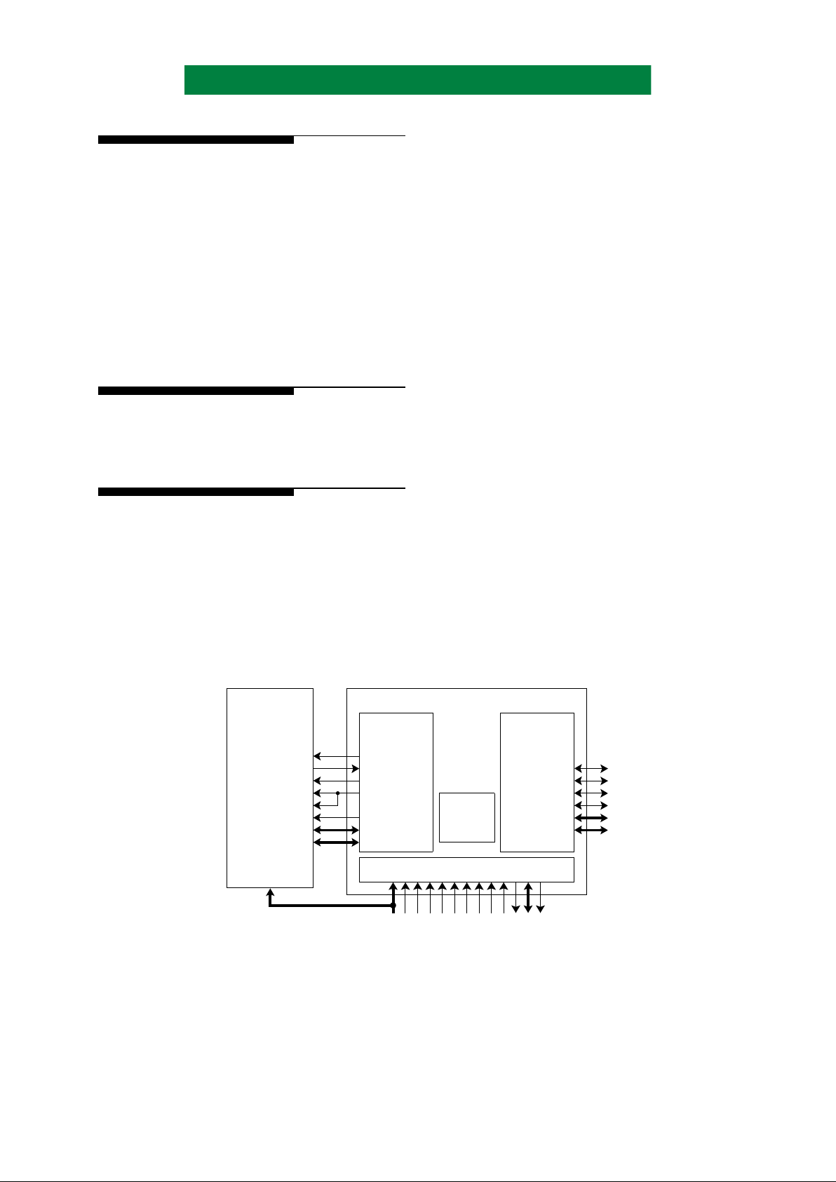
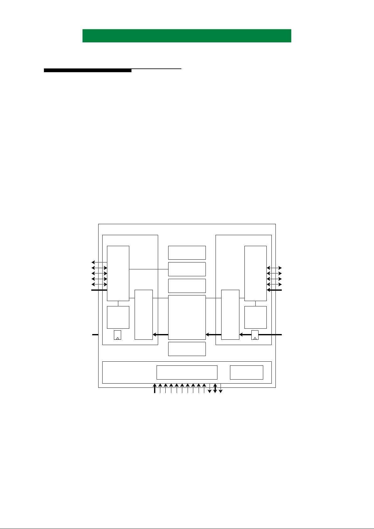
2.2.3 DECOMPRESSION MODE
During decompression mode, compressed data
flows into Port B. It is then uncompressed by the
DCLZ engine. The resulting uncompressed data is
then transferred out of Port A.
The compressed data is partitioned into records,
with End of Record codewords embedded in the
compressed data. Multiple records can be
automatically decompressed, by programming the
number of records into the Record Coun t register . A
decompression sequence has been completed after
the last byte of the last record has been
uncompressed and then transferred out of Port A.
This event sets the Port A End of T r ansfer int errupt.
The following sequence is used to p rogram the
chip to decompress multiple records:
- Program Record Count register
- Program Interrupt Disable register
- Enable PORT A END OF TRANSFER Interrupt
- Program DCLZ Control register
DCLZ MODE[2:0] Decompression
COMP RATIO OPT ENABLE 0
RESET DICT AFTER EOR 0
RESET DICT 0
PAUSE AFTER EOR 0
PAUSE 0
- The PORT A END OF TRANSFER Interrupt signals
decompression completed
Figure 7: Decompression Mode
PORT A
BYTE
COUNTER
PORT B
BYTE
COUNTER
PORT A
DMA
STATE
MACHINE
PORT A
FIFO
PORT B
DMA
STATE
MACHINE
PORT B
FIFO
SINGLE DATA
BUS ARBITER
RECORD COUNT
REGISTER
RECORD LENGTH
REGISTER
PROCESSOR INTERFACE
STATE MACHINE
PASS THROUGH
CONTROLLER
INTERRUPT
LOGIC
PROCESSOR
INTERFACE
DCLZ
ENGINE
PORT A INTERFACE PORT B INTERFACE
ACSN
DREQA
DACKA
AOE
AWE
DAPTY[1:0]
DA[15:0]
A[4:0]
PORTA CSN
CSN
RWN/IOWRN
DSN/IORDN
PROCMODE
TRISTATEN
TEST
RESTN
CLK
DTACKN/READY
D[7:0]
INTN/INT
DREQB
DACKB
BOE
BWE
DBPTY[1:0]
DB[15:0]
(8 Bytes) (8 Bytes)
AHA3210B Compression Chip
Page 8 of 45 PS3210B-1299
Advanced Hardware Architectures, Inc.
2.2.4 DECOMPRESSION OUTPUT DISABLED
MODE
The DCLZ algorithm allows the compression
dictionary to be shared between multiple records.
To decompress records in the middle of a multiple
record sequence, the pr eceding records must first be
decompressed, in order to properly build the
compression dictionary.
Decompression output disabled mode allows
the preceding records to be decompressed, while
discarding the unwanted un compr essed data. Once
this is completed, the chip can be programmed to
decompression mode, to decompr ess and output the
desired records.
In decompression output disabled mode, the
data is discarded between the Port A Interface and
the Port A pins. Port A DMA remains inactive . The
Port B Byte Counter, the Port A Byte Counter, the
Port B Interface Byte Count, the Port A Interface
Byte Count, the Record Count regis ter , and the Port
A End of Transfer Interrupt operate as in
decompression mode. It is recommended that the
Port A Interface be empty and th e chip paused
before switching between decompression output
disabled and decompression modes.
The following sequence is used to p rog ram the
chip to decompress multiple records in output
disabled mode:
- Program Record Count register
- Program Interrupt Disable register
- Enable PORT A END OF TRANSFER Interrupt
- Program DCLZ Control register
DCLZ MODE[2:0] Decomp; Output
Disabled Mode
COMP RATIO OPT ENABLE 0
RESET DICT AFTER EOR 0
RESET DICT 0
PAUSE AFTER EOR 0
PAUSE 0
- The PORT A END OF TRANSFER Interrupt signals
decompression output disabled completed
Figure 8: Decompression Output Disabled Mode
PORT A
BYTE
COUNTER
PORT B
BYTE
COUNTER
PORT A
DMA
STATE
MACHINE
PORT A
FIFO
PORT B
DMA
STATE
MACHINE
PORT B
FIFO
SINGLE DATA
BUS ARBITER
RECORD COUNT
REGISTER
RECORD LENGTH
REGISTER
PROCESSOR INTERFACE
STATE MACHINE
PASS THROUGH
CONTROLLER
INTERRUPT
LOGIC
PROCESSOR
INTERFACE
DCLZ
ENGINE
PORT A INTERFACE PORT B INTERFACE
ACSN
DREQA
DACKA
AOE
AWE
DAPTY[1:0]
DA[15:0]
A[4:0]
PORTA CSN
CSN
RWN/IOWRN
DSN/IORDN
PROCMODE
TRISTATEN
TEST
RESTN
CLK
DTACKN/READY
D[7:0]
INTN/INT
DREQB
DACKB
BOE
BWE
DBPTY[1:0]
DB[15:0]
(8 Bytes) (8 Bytes)
AHA3210B Compression Chip
PS3210B-1299 Page 9 of 45
Advanced Hardware Architectures, Inc.
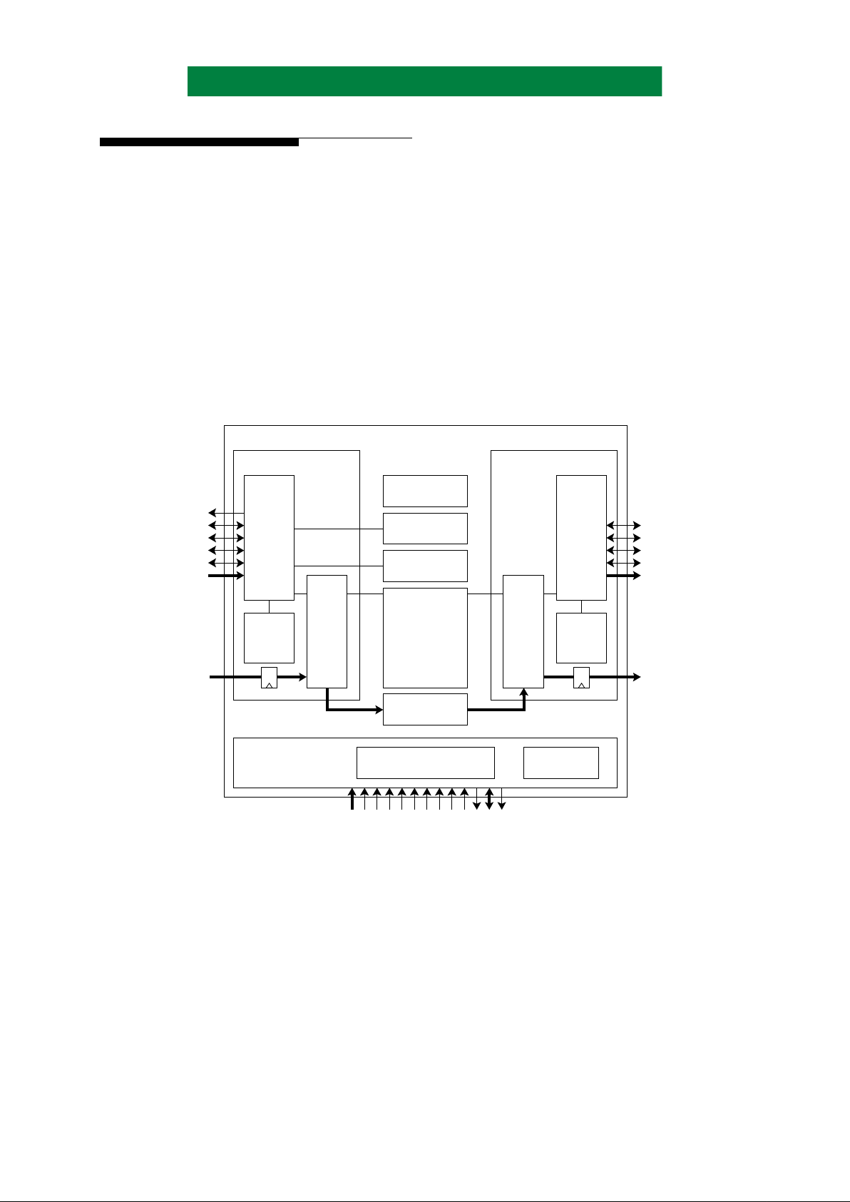
2.2.5 PASS THROUGH A TO B MODE
During pass through A to B mode, data enters
Port A, is transferred through the Port A Interface
and the Port B Interface, and then transferred out of
Port B. The data is not altered as it passes through
the chip.
The Record Le ngth register determines the
number of bytes in a record. The Record Count
register determines the number of records. Multiply
the values of these two registers to determine the
total number of bytes that will be transferred
through the chip. The pass through sequence has
been completed after the last byte of the last record
has been transferred out of Port B. This event sets
the Port B End of Transfer interrupt.
The following sequence is used to p rogram the
chip to pass through data from Port A to Port B:
- Program Record Length register
- Program Record Count register
- Program Interrupt Disable register
- Enable PORT B END OF TRANSFER Interrupt
- Program DCLZ Control register
DCLZ MODE[2:0] Pass through A to B
COMP RATIO OPT ENABLE 0
RESET DICT AFTER EOR 0
RESET DICT 0
PAUSE AFTER EOR 0
PAUSE 0
- The PORT B END OF TRANSFER interrupt signals pass
through A to B completed
Figure 9: Pass Through A to B Mode
PORT A
BYTE
COUNTER
PORT B
BYTE
COUNTER
PORT A
DMA
STATE
MACHINE
PORT A
FIFO
PORT B
DMA
STATE
MACHINE
PORT B
FIFO
SINGLE DATA
BUS ARBITER
RECORD COUNT
REGISTER
RECORD LENGTH
REGISTER
PROCESSOR INTERFACE
STATE MACHINE
PASS THROUGH
CONTROLLER
INTERRUPT
LOGIC
PROCESSOR
INTERFACE
DCLZ
ENGINE
PORT A INTERFACE PORT B INTERFACE
ACSN
DREQA
DACKA
AOE
AWE
DAPTY[1:0]
DA[15:0]
A[4:0]
PORTACSN
CSN
RWN/IOWRN
DSN/IORDN
PROCMODE
TRISTATEN
TEST
RESTN
CLK
DTACKN/READY
D[7:0]
INTN/INT
DREQB
DACKB
BOE
BWE
DBPTY[1:0]
DB[15:0]
(8 Bytes) (8 Bytes)
AHA3210B Compression Chip

Page 10 of 45 PS3210B-1299
Advanced Hardware Architectures, Inc.
2.2.6 PASS THROUGH B TO A MODE
During pass through B to A mode, data enters
Port B, is transferred through the Port B Interface
and Port A In terface, and is then transferred out of
Port A. The data is not altered as it passes through
the chip.
The Record Le ngth register determines the
number of bytes in a record. The Record Count
register determines the number of records. Multiply
the values of these two registers to determine the
total number of bytes that will be transferred
through the chip. The pass through sequence has
been completed after the last byte of the last record
has been transferred out of Port A. This event sets
the Port A End of Transfer interrupt.
The following sequence is used to p rogram the
chip to pass through data from Port B to Port A:
- Program Record Length register
- Program Record Count register
- Program Interrupt Disable register
- Enable PORT A END OF TRANSFER Interrupt
- Program DCLZ Control register
DCLZ MODE[2:0] Pass through B to A
COMP RATIO OPT ENABLE 0
RESET DICT AFTER EOR 0
RESET DICT 0
PAUSE AFTER EOR 0
PAUSE 0
- The PORT A END OF TRANSFER interrupt signals pass
through B to A completed
Figure 10: Pass Through B to A Mode
PORT A
BYTE
COUNTER
PORT B
BYTE
COUNTER
PORT A
DMA
STATE
MACHINE
PORT A
FIFO
PORT B
DMA
STATE
MACHINE
PORT B
FIFO
SINGLE DATA
BUS ARBITER
RECORD COUNT
REGISTER
RECORD LENGTH
REGISTER
PROCESSOR INTERFACE
STATE MACHINE
PASS THROUGH
CONTROLLER
INTERRUPT
LOGIC
PROCESSOR
INTERFACE
DCLZ
ENGINE
PORT A INTERFACE PORT B INTERFACE
ACSN
DREQA
DACKA
AOE
AWE
DAPTY[1:0]
DA[15:0]
A[4:0]
PORTACSN
CSN
RWN/IOWRN
DSN/IORDN
PROCMODE
TRISTATEN
TEST
RESTN
CLK
DTACKN/READY
D[7:0]
INTN/INT
DREQB
DACKB
BOE
BWE
DBPTY[1:0]
DB[15:0]
(8 Bytes) (8 Bytes)
AHA3210B Compression Chip
 Loading...