

Advanced Analog Technology, Inc.
AAT602
DD
V
Product information presenting is current as of publication date. Details are subject to change without notice.
HIGH-PRECISION RESET VOLTAGE DETECTOR
FFFFEA
EATURES
TURES
EAEA
TURESTURES
GENERAL DESCRIPTION
GENERAL DESCRIPTION
GENERAL DESCRIPTIONGENERAL DESCRIPTION
May 2008
Low Current Consumption
(3µA typical,
High-Precision Reset Voltage ±2%
Hysteresis Voltage 5% Typical
Reset Voltage 1.8V to 5.5V
Fixed or Adjustable Delay Time
Open Drain or Push-Pull Output
External Delay Time
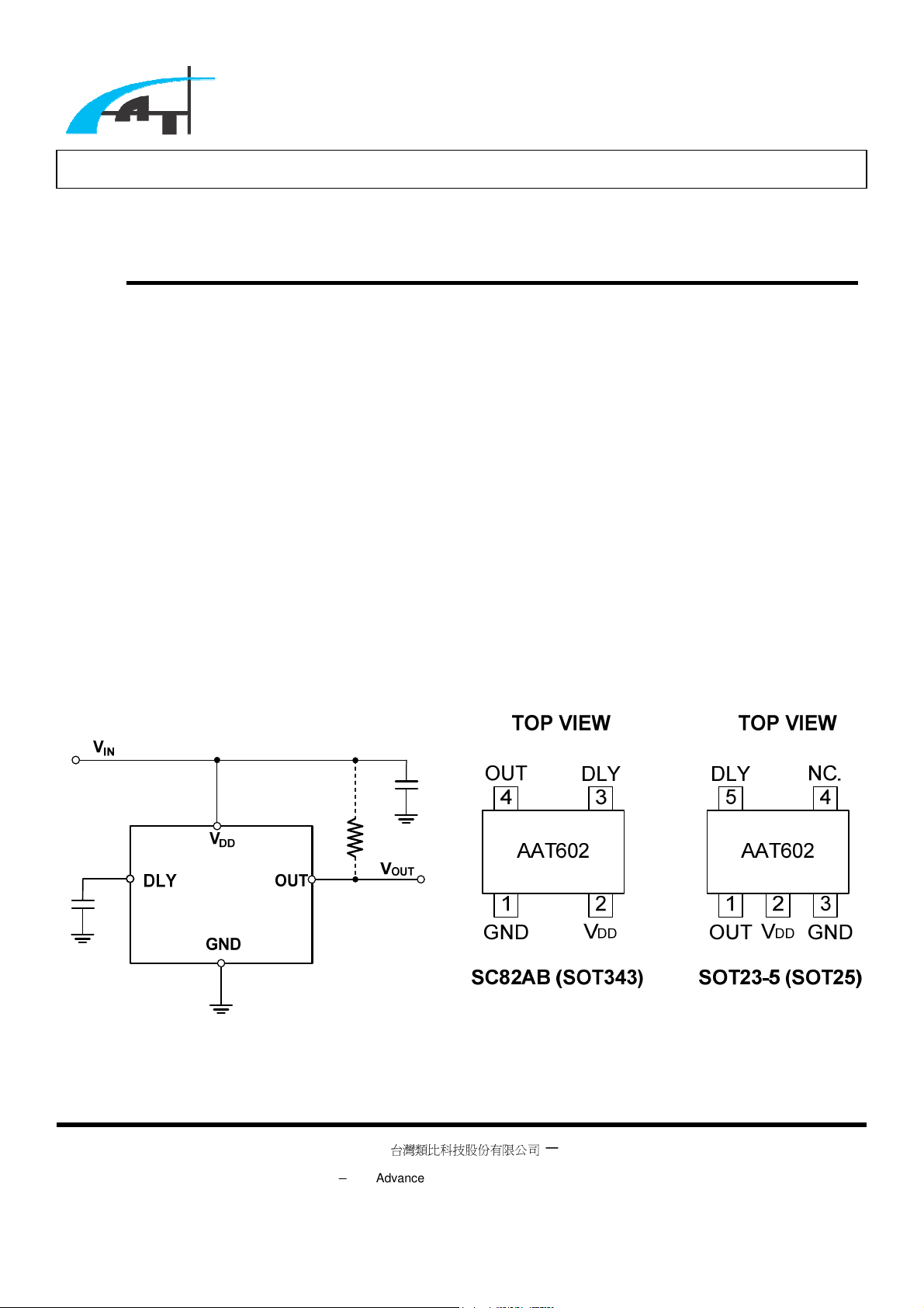
SC82AB (SOT343), SOT23-5 (SOT25)
Package Available
APPLICATION
APPLICATION
APPLICATIONAPPLICATION
=3V)
The AAT602 is a reset voltage detector that provides a
high-precision output signal, which allows users to
initiate or reset the system.
The detection voltage with an accuracy of ±2% is
trimmed to customized specification. Delay time can be
adjusted by an external capacitor. And output signal may
be configured as either open drain or push-pull.
With minimal external components required, the AAT602
offers a simple and economical solution.
PPPPIN CONFIGURATION
IN CONFIGURATION
IN CONFIGURATIONIN CONFIGURATION
–
台灣類比科技股份有限公司
–
Advanced Analog Technology, Inc.
Version 5.00
Page 1 of 8
–
–
Advanced Analog Technology, Inc.
AAT602
DD
V
DD
V
I
V
DD
V
C
T
20
−
C
C
C
storage
45
−
C
C
C
J
T
C
JA
θ
C
JA
θ
C
C
T
C
d
P
C
T
C
d
P
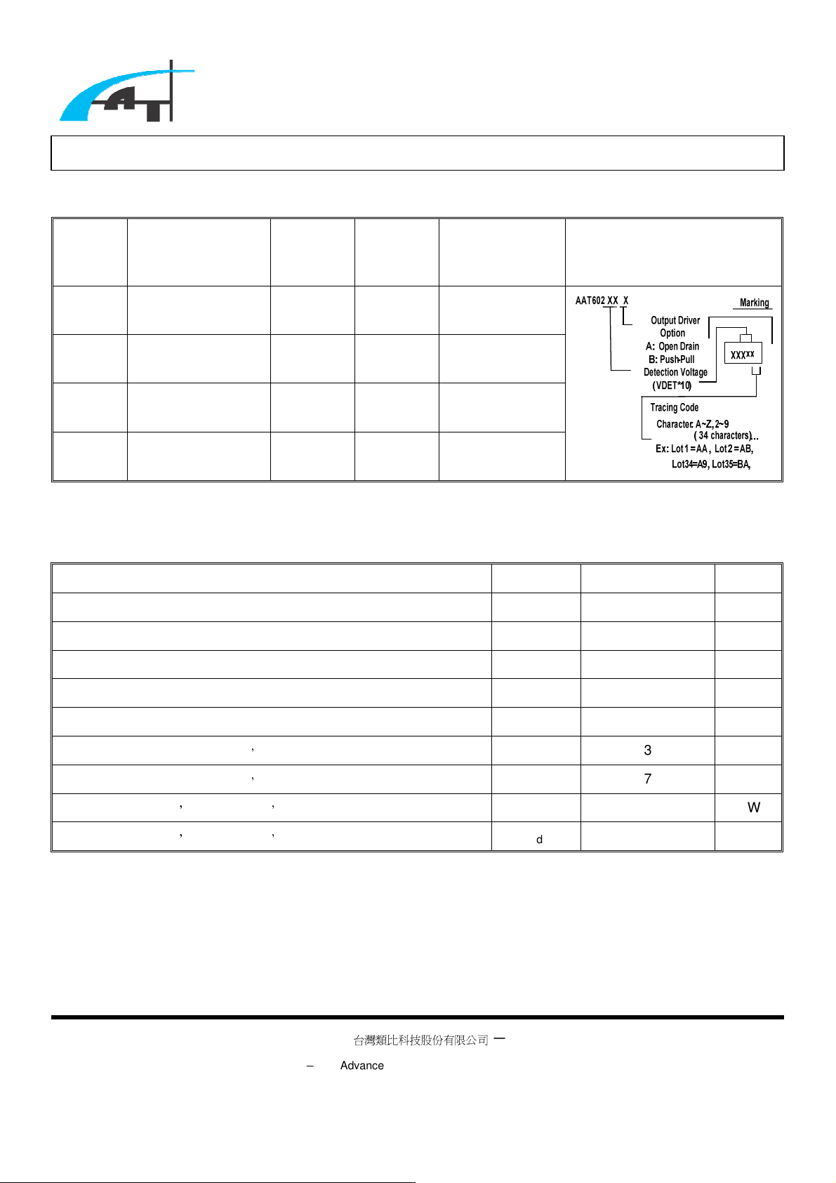
ORDERING INFORMATIO
ORDERING INFORMATIONNNN
ORDERING INFORMATIOORDERING INFORMATIO
May 2008
DEVICE
TYPE
AAT602 AAT602XXA-S5-T
AAT602 AAT602XXB-S5-T
AAT602 AAT602XXA-S15-T
AAT602 AAT602XXB-S15-T
NOTE1: All AAT products are lead free and halogen free
AAAABSOLUTE
BSOLUTE MMMMAXIMU
BSOLUTE BSOLUTE
OUT to GND
,
Input Voltage (DLY)
PART NUMBER PACKAGE PACKING
S5:SOT
23-5
(SOT25)
S5:SOT
23-5
(SOT25)
S15:
SC
82AB
S15:
SC
82AB
AXIMUMMMM R
AXIMUAXIMU
PARAMETER SYMBOL VALUE UNIT
RATINGS
ATINGS
R R
ATINGSATINGS
T: Tape
and reel
T: Tape
and reel
T: Tape
and reel
T: Tape
and reel
TEMP.
RANGE
20−C°
20−C°
20−C°
20−C°
to+85
to+85
to+85
to+85
MARKING
DESCRIPTION
C°
C°
C°
C°
7 V
+0.3
V
Operating Free-Air Temperature Range
Storage Temperature Range
Maximum Junction Temperature
Package Thermal Resistance,SC82AB
Package Thermal Resistance,SOT23−5
Power Dissipation,@
Power Dissipation,@
=25
=25
°
,
°
,
SC82AB
SOT23−5
–
–
台灣類比科技股份有限公司
Advanced Analog Technology, Inc
–
T
.
–
°
to +85
°
°
to +125
+125
333
275
300 mW
364 mW
°
°
°
°
°
/W
°
/W
Version 5.00
Page 2 of 8
Advanced Analog Technology, Inc.
AAT
602
C
DET
DET
2%
DET
HYS
DET
DET
DET
DD
I
DD
V
A
OP
V
L
I
DD
V
OUT
A
OL
V
OUT
OH
V
OUT
1.2
−
DD
V
0.2
D
t
DD
V
DET
0.3
5
DD
V
EEEELECTRICAL CHARACTERISTICS
LECTRICAL CHARACTERISTICS
LECTRICAL CHARACTERISTICSLECTRICAL CHARACTERISTICS
(TC = 25
Recommended Operating Conditions
Detection Voltage
Hysteresis Voltage
Supply Current
Operating Voltage
°
)
PARAMETER SYMBOL
V
V
CONDITION
TEST
=3V
0.9 5.5 V
MIN TYP MAX UNIT
V
−
V
x3%
3 5
V
x5%
V
+2%
V
x8%
May 2008
V
V
µ
Open Drain Leakage Current
Push-Pull Output Voltage
External Delay Time
V
I
I
=
V
= 5.5V,
= 5.5V
= 1.2mA
=
−
mA
V
PIN DESCRIPTION
PIN DESCRIPTION
PIN DESCRIPTIONPIN DESCRIPTION
PIN NO.
SC82AB
(SOT343)
1 3 GND - Ground
2 2
3 5 DLY I Delay Capacitor Connection Pin
4 1 OUT O Open Drain or Push-Pull Output
SOT23-
(SOT25)
NAME
I/O DESCRIPTION
- Power Input / Detection Voltage
0.1
0.2 V
−
V
250 320 390 ms
V
µ
–
台灣類比科技股份有限公司
–
Advanced Analog Technology, Inc.
Version 5.00
Page 3 of 8
–
–

Advanced Analog Technology, Inc.
AAT
602
FUNCTION
FUNCTION BLOCK DIAGRAM
FUNCTIONFUNCTION
BLOCK DIAGRAM
BLOCK DIAGRAMBLOCK DIAGRAM
May 2008
TYPICAL
TYPICAL AAAAPPLICATION CIRCUIT
TYPICALTYPICAL
PPLICATION CIRCUIT
PPLICATION CIRCUITPPLICATION CIRCUIT
–
台灣類比科技股份有限公司
–
Advanced Analog Technology, Inc.
Version 5.00
Page 4 of 8
–
–

Advanced Analog Technology, Inc.
AAT
602
PPPPART
ART NNNNUMBER
ART ART
AAT60218A AAT60233A AAT60248A
AAT60218B AAT60233B AAT60248B
AAT60219A AAT60234A AAT60249A
AAT60219B AAT60234B AAT60249B
AAT60220A AAT60235A AAT60250A
AAT60220B AAT60235B AAT60250B
AAT60221A AAT60236A AAT60251A
AAT60221B AAT60236B AAT60251B
AAT60222A AAT60237A AAT60252A
AAT60222B AAT60237B AAT60252B
AAT60223A AAT60238A AAT60253A
AAT60223B AAT60238B AAT60253B
UMBER AAAAVAILABLE
UMBERUMBER
VAILABLE
VAILABLEVAILABLE
May 2008
AAT60224A AAT60239A AAT60254A
AAT60224B AAT60239B AAT60254B
AAT60225A AAT60240A AAT60255A
AAT60225B AAT60240B AAT60255B
AAT60226A AAT60241A
AAT60226B AAT60241B
AAT60227A AAT60242A
AAT60227B AAT60242B
AAT60228A AAT60243A
AAT60228B AAT60243B
AAT60229A AAT60244A
AAT60229B AAT60244B
AAT60230A AAT60245A
AAT60230B AAT60245B
AAT60231A AAT60246A
AAT60231B AAT60246B
AAT60232A AAT60247A
AAT60232B AAT60247B
–
台灣類比科技股份有限公司
–
Advanced Analog Technology, Inc.
Version 5.00
Page 5 of 8
–
–

Advanced Analog Technology, Inc.
AAT
602
TIMING CHART
TIMING CHART
TIMING CHARTTIMING CHART
V
DD
V
DET
V
DET
V
OP
GND
+ V
HYS
May 2008
Initial Voltage: High
Active : Low
V
keeps high when
OUT
V
goes from low to high
DD
V
OUT
V
DET
V
DET
V
OP
GND
t
D
Beginning to detect V
+ V
DET
HYS
–
台灣類比科技股份有限公司
–
Advanced Analog Technology, Inc.
Version 5.00
Page 6 of 8
–
–

Advanced Analog Technology, Inc.
AAT
602
PACK
PACKAAAAGE
PACKPACK
SC82AB (SOT343)
GE DDDDIMENSION
GE GE
IMENSION
IMENSIONIMENSION
May 2008
Symbol
A 0.8 ------ 1.1
A1 0.0 ------ 0.1
A2 0.7 0.9 1.0
b 0.25 0.30 0.40
b1 0.35 0.40 0.50
c 0.10 ------ 0.26
D 1.8 2.0 2.2
E1 1.15 1.25 1.35
E 1.8 2.1 2.4
e 1.30 BSC
L 0.26 0.36 0.46
L2 0.15 BSC
y ------ ------ 0.1
θ 0˚ ------ 8˚
θ1 4˚ ------ 12˚
Dimensions In Millimeters
MIN TYP MAX
–
台灣類比科技股份有限公司
–
Advanced Analog Technology, Inc.
Version 5.00
Page 7 of 8
–
–

AAT
602
PACK
PACKAAAAGE
PACKPACK
SOT23-5 (SOT25)
GE DDDDIMENSION
GE GE
IMENSION
IMENSIONIMENSION
Advanced Analog Technology, Inc.
May 2008
Symbol
A 1.05 1.2 1.3
A1 ------ ------ 0.15
A2 1 1.1 1.15
b 0.3 ------ 0.5
c 0.08 ------ 0.22
D 2.90 BSC
E 2.80 BSC
E1 1.60 BSC
e 0.95 BSC
e1 1.90 BSC
L 0.30 0.45 0.60
L1 0.60 REF
L2 0.25 BSC
R 0.1 ------ ------
R1 0.10 ------ 0.25
θ 0˚ 4˚ 8˚
θ1 5˚ 10˚ 15˚
Dimensions In Millimeters
MIN TYP MAX
–
台灣類比科技股份有限公司
–
Advanced Analog Technology, Inc.
Version 5.00
Page 8 of 8
–
–
 Loading...