

Page 1

SYN T H ET IS E UR DE FREQUENCE
FREQUENCY SYNTHESIZER
0, 0 1 Hz/200 kHz
3100 B
ADRET
Schlumberger
12, avenue Vladimir Komarov • B.P. 33 78192 Trappes Cedex • France • Tel. 30.51:29.72
Telefax 30.51.00.74 • Telex AD RFL 697821 F • Siret 679805077-00048 • ( XT Paris 21 797 04
Page 2

r
ADRET
SYNTH ETISEUR DE FREQUENCE
FREQUENCY SYNTHESIZER
0,01 Hz/200 kHz
ADRET
Schlumberger
3100 B
12, avenue Vladimir Komarov • B.P. 33 78192 Trap pes Cedex • France • Tel. 30. 51. 29.72
Telefax 30.5 1.00.74 • Telex A D R EL 697821 F • Siret 679805077-00048 • CC P Paris 2 1 797 04
Page 3

E R R A T A No_j_______________________
Date _ - J UUL 12IU _ 1973
Valid from serial No _1 3 _
_________________________________
------------------------------------------------------------
Date of delivery________________________________________
CONCERNS INSTRUCTIONS MANUAL FOR _ IID Q Bl ANJL QP J1 QWS
Edition. _2 t AQ____________________________________________
Page
or plate
PLATE
VI-7
INSTEAD OF
Q3 : 2N 2219
Q6 : 2N 2905
Q7 : 2N 2219
Q12 : 2N 2905
CR5, CR6, CRll
and CR12 : IN 4448
Q3 : BD 135
Q6 : BD 136
Q7 : BD 135
Q12 : BD 136
Trans i st ors BC 184C
whose c ol lector and b a se
READ
PLATE
VI-18
Q15 : 2N 2219
Q16 : 2N 2905
CR9 : IN 4448
CR10 : IN 4448
a r e short-circui ted.
Q15 : BD 135
Q16 : BD 136
T ran si stors BC 184C
whose col l ector and b as e
ar e shor t-circui t ed.
j
|
3 3 0/ 226
Page 4

S U M M A R Y
Page
CHAPTER I FUNCTIONAL DESCRIPTION
CHAPTER II SPECIFICATIONS
I I - l SPECIFICATIONS OF SYNTHESIZER 3 » B I I - I
I I -2 SPECIFICATIONS OF OPTION 3111B II-4
11-3 SPECIFICATIONS OF OPTION 3112B H-5
I I-4 SPECIFICATIONS OF OPTION 3114B II- 6
CHAPTER I I I PRINCIPLE OF OPERATION
I I I - l GENERATOR SYNTHESIZER 3100B H I-1
I I I -2 OPTION 3111B H I-1
111-3 OPTION 3112B H I-2
I I I -4 OPTION 3114B H I-2
CHAPTER IV PRELIMINARY INSTRUCTIONS
IV-1 AC LINE CONNECTION IV-1
IV-2 MOUNTING IN 19" RACK IV-1
CHAPTER V OPERATING INSTRUCTIONS
V-l EXTERNAL DESCRIPTION V-l
V-2 3100B OPERATING INSTRUCTIONS V-l
V-2-1 Switching on V-l
V-2-2 Local Mode V-l
V-2-3 Remote Mode V-2
V-2-4 Output signals V-3
V-2-5 Reference frequency V-4
V-2-6 Supply voltages output V-5
V-3 3111B OPERATING INSTRUCTIONS V-6
V-3-1 Local Mode V-6
V-3-2 Remote Mode V-6
V-4 3112B OPERATING INSTRUCTIONS V-7
V-4-1 Local Mode V-7
V-4-2 Remote Mode V-8
V-4-3 Output signal V-8
V-5 3114B OPERATING INSTRUCTIONS V-9
V-5-1 Search function V-9
V-5-2 Free-run mode V-10
V-5-3 Triggered mode
V-5-4 External mode
v-
v-
12
14
- 1 -
Page 5

CHAPTER VI
VI-1
VI-2
VI-3
VI-4
VI-5
VI-6
VI-7
VI-8
VI-9
VI-10
VI-10-1
VI-10-2
VI-10-3
V I-U
VI-11-1
CIRCUIT DESCRIPTION
INTRODUCTION
CENTADE
STANDARD DECADE
TWENTY-INCREMENT UNIT
OUTPUT MIXER
FUNCTION SWITCH
OUTPUT AMPLIFIER
TIME BASE
PROGRAMMABLE ATTENUATOR OPTION 3111B
PROGRAMMABLE PHASE-SHIFTER OPTION 3112B
Digital Phase-Shift
Generation sin <t> / cos <p
Output Circu it
SEARCH AND SWEEP OPTION 3114B
Sweep
VI-11-2 Interpolation
VI-1
VI-2
VI-5
VI-7
VI-10
VI-11
VI-11
VI-11
VI-12
VI-13
VI-14
VI-14
VI-15
VI-15
VI-16
VI-16
OPTION IEEE BUS OPERATING INSTRUCTIONS
CHAPTER VII MAINTENANCE
CHAPTER V III
PLATES, SCHEMATICS, PARTS LIST
V I-1 8
- 2 -
Page 6

L IS T O F P L A TE S
Plate I I I - l
V- 1
ate
P
P ate V-
P ateV-3 OPTION 3111B - FRONT AND REAR-PANEL DESCRIPTION
P
P
P
P ate
P ate V
P ate
P
P ate V -5
P
P
P ate
P ate
P ate
P ate V -11 CODE FILTER
P ate
P ate
P
P
P ate
P
P
P
P
2 3100B - REAR PANEL DESCRIPTION
4
ate V-
ateV-5 OPTION 3114B - FRONT AND REAR-PANEL DESCRIPTION
ate V-•6 INTERNAL DESCRIPTION
V -1
-2 3111B - 3112B - 3114B BLOCK DIAGRAM
V -3 CENTADE
V -4 STANDARD DECADE
ate
ate V -6 OUTPUT MIXER
ate V -7
-8
V
V -9
V -10 SWITCH TRANSCODING
-12 3U POWER SUPPLY
V
V -13 PROGRAMMABLE ATTENUATOR (Option 311IB)
V -14 SWITCH DECODING (Option 3111B)
ate
V -15
ate
V -16 DIGITAL PHASE-SHIFT (Option 3112B)
V -17 GENERATION Sin <j,/Cos <t> (Option 3112B) .
ate
-18 OUTPUT CIRCUIT (Option 3112B)
V
ate
V -19 SWEEP (Option 3114B)
ate
V -20 INTERPOLATION (Option 3114B)
ate
PRINCIPLE OF OPERATION
3100B - FRONT PANEL DESCRIPTION
OPTION 3112B - FRONT AND REAR-PANEL DESCRIPTION
3100B BLOCK DIAGRAM
TWENTY-INCREMENT UNIT
OUTPUT AMPLIFIER
TIME BASE
ATTENUATOR/FUNCTION SWITCH
CODE FILTER (Options 3111B and 3112B)
Page 7

I F U N C T I O N A L D E S C R IP T I O N
The 3100B AORET synthesizer is a d ig itally controlled signal generator which delivers all 0.01 Hz
to 200 kHz frequencies with 0.01 Hz resolution.
The synthesized frequency can be either manually dia lle d through eight rotary switches on the
front panel of the instrument (Local mode), or programmed in parallel BCD code through TTL signals sent
to the programming connector on the rear panel of the instrument (Remote mode).
Two channels A and B simultaneously deliver two output signals in phase quadrature with 5 n or
50 a impedance and an electromotive force adjustable from 0 to 10 Vpeak. Moreover, the signal delivered
by channel A can have the following forms : sine wave, positivd square wave, symmetrical square wave,
negative square wave, TTL level square wave.
According to the user's needs, the 3100B generator synthesizer can be fitte d with the following
options :
- Option 311IB : progranmable attenuator
This option allows to attenuate one of the output signals of the generator synthesizer from 0 dB
to 79.9 dB with 0.1 dB resolution. The attenuation value can be either manually dialled through three
rotary switches in Local mode, or programmed in parallel BCD code through TTL signals in Remote mode.
- Option 3112B : programmable phase-shifter
This option delivers a sinusoidal signal phase-shifted from 0° to 359.9° with regard to the signal
of channel A of the 3100B generator synthesizer. The phase-shift value can be eithe r manually dialled
through four thumbwheel switches in Local mode, or programmed in pa rallel BCO code through TTL signals in
Remote mode. The electrom otive force of the phase-shifted signal is adjustable from 0 to 10 Vpeak with
5 ft or 50 ft output impedance.
- Option 3114B : Search and Sweep
This option allows progressive frequency variation of the generator synthesizer output signals.
Four modes of operation are possible depending on the function required :
- Search function
- Free-run Sweep
- Triggered Sweep
- Search or Sweep by external signal
In all cases, twenty-one "birdy" or re ctified markers display the frequency variation achieved.
1-1
Page 8

II S P ECI FICAT IONS
I I - l SPECIFICATIONS OF SYNTHESIZER 3100B
FREQUENCY
Range : O.Ol Hz to 199 999.99 Hz
Resolution : 0.01 Hz
Selection : with 8 dig its
S ta bility : ± 2.10~5 from 0°C to + 50°C
+ 5.10- ? per day afte r 8 hours'operation.
EXTERNAL REFERENCE
Substitution of the bu ilt-in master oscillator for the external reference.
Frequency : 10 MHz
Level : 50 mVrms to 1 Vrms/50 n.
10 MHz REFERENCE OUTPUT
Level : 100 mVrms/50 fi.
OUTPUT SIGNALS
The synthesized signal is simultaneously available on four diffe rent outputs :
Main output A : Provides sine wave, positive , negative , symmetrical or
TTL square wave.
Main output B : Sine wave, phase-shifted from + 90° with respect to the outputs A wave.
A u x ilia r y o u tput A : sine wave.
A u x ilia r y o utpu t B : sine wave, phase-shifted from + 90° with respect to the outputs A wave.
MAIN OUTPUT A
Provides sine wave, positive, negative, symmetrical or TTL square wave.
• Square waves rise and f a ll time : 100 ns
• Square waves duty cycle : 50 % + 2 %
Output level :
• Sine wave :
e.m.f. variable : 0 V to 10 V peak
e.m.f. calibrated : 7 V peak + 5 %
• Positive or negative square wave :
e.m.f. variable : 0 V to 10 Vp-p
e.m .f. calibrated : 7 Vp-p ± 5 %
II-l
Page 9

• Symmetrical square wave :
e.m.f. variable : 0 V to 10 V peak
e.m .f. calibrated : 7 V peak ± 5 %
• TTL square waves :
e.m.f. calibrated : 3.8 V p-p ± 5 %
Output level flatness : + 3 % within the entire frequency range.
Output impedance : 50 n or 5 n
Output current : maximum 100 mA peak
Output level attenuation (50
• Dynamic range : 70 dB
• Resolution : 10 dB
• Accuracy : + 0.5 dB
MAIN OUTPUT B
Sine wave with 90° phase-shift from main output signal.
Phase-shift accuracy with respect to main output sine wave with calibrated e.m .f. : + 0.5°
Output level :
• e.m .f. variable : 0 V to 10 V peak
• e.m .f. calibrated : 7 V peak + 5 %
Output level flatness : ± 3 % within the entire frequency range.
Output impedance : 50 n or 5 a
Output current : maximum 100 mA peak
AUXILIARY OUTPUT A
Sine wave in phase with main output A.
n impedance) :
Output level : 2 Vpeak e.m .f.
Load impedance : 1 kft minimum
AUXILIARY OUTPUT B
Sine wave with 90° phase-shift from signal of auxiliary output A.
Output level : 2 Vpeak e.m .f.
Load impedance : 1 kft minimum
SPECTRAL PURITY
(measured on main outputs with calibrated e.m .f. and 50 fl impedance)
Sine wave harmonic signals : - 50 dB
Non-harmonic signals : - .70 dB
Phase noise in a 1 Hz band :
- 110 dB at 100 Hz from carrier
- 115 dB at 1 kHz from c arrie r
- 125 dB at 10 kHz from carrie r.
11-2
Page 10

FREQUENCY PROGRAMMING
Selection of the Local or Remote mode is achieved eith er through a front-panel switch or through
a rear-panel programming connector, with prio rity for the Remote mode.
• Current-source positive TTL logic :
"1" level : + 2 V to + 5 V/0.1 mA
"0" level : 0 V to + 0.4 V/0.2 mA
• 1-2-4-8 parallel BCD code
• Resolution : 0.01 Hz
• Settling times :
Digits affected by
frequency switching
The above-mentioned settling times depend, only on the weight of the digits
affected by frequency switching.
POWER REQUIREMENTS
Voltage : 115 V/230 V (+ 10 %)
Frequency : 50 Hz to 400 Hz
Consumption : 40 VA
105 Hz
to 103 Hz
Less than
or equal to
102 Hz
Settling time at 100 Hz
from fina l frequency
0.5 ms
Frequency error less than 1 Hz
afte r 1 ms
Settling time at 10 Hz
from fin al frequency
1 ms
MECHANICAL DATA
Adaptable to 19" rack
Height : 132 mm (3U)
Width : 440 mm
Overall depth : 452 mm
Weight : 10 kg to 12 kg according to options.
TEMPERATURE RANGE
Operation : 0°C to + 50°C
Storage : - 20°C to + 70°C
11-3
Page 11

11-2 S P E C IF I CA T IO N S OF O P T I O N 31 1 1 B
ATTENUATION
Dynamic range : 79.9 dB
Resolution : 0.1 dB
Selection : by 3 rotary switches
Characteristic impedance : 50 n
Accuracy :
• 0.1 dB steps : + 0.05 dB
• 1 dB steps : + 0.1 dB
• 10 dB steps : + 0.2 dB
• Maximum error : ± 1 dB
MAXIMUM PHASE-SHIFT
PROGRAMMING
• • Current-source positive TTL logic :
"1"
level : +
"0"
level
• 1-2-4-8 parallel BCD code
• Resolution : 0.1 dB
« Switching time : 3 ms
2 V
: 0 V
to + 5
to
+ 0.4 V/ 0.2
V/0.1
mA
mA
Page 12

11-3 S P E C I FI CAT IO N S O F O P T I O N 3 1 1 2 B
PHASE-SHIFT
Range : 0° to 359.9°
Resolution : 0.1°
Selection : by 4 thumbwheel switches
Phase-shift accuracy : measured with respect to the main output A sine wave, with calibrated e.m .f.
and 50 fi impedance.
• Linearity : + 1°
• Phase/frequency response : + 1°
• Phase/temperature response : + 0.025 degree/°C
OUTPUT LEVEL
Waveform : sine wave
Output level :
• e.m .f. variable : 0 V to 10 Vpeak
• e.m.f. calibrated : 7 V peak + 5 %
»
Output level flatness : + 3 % within the entire frequency range
Output impedance : 50 n or 5 n
Output current : maximum 100 mA peak
SPECTRAL PURITY
(measured with calibrated e.m .f. and 50 n impedance)
Harmonic signals : - 45 dB
Non-harmonic signals : - 65 dB
Phase-noise in a 1 Hz band :
- 110 dB at 100 Hz from carrier
- 115 dB at 1 kHz from carrier
PHASE-SHIFT PROGRAMMING
• Current-source positive TTL logic :
“1" level : + 2 V to + 5 V/0.1 mA
"0" level : 0 V to + 0.4 V/ 0.2 mA
• 1-2-4-8 parallel BCD code
• Resolution : 0.1°
• Switching time : 20 ms
11-5
Page 13

11-4 SP ECIFI CA TIO NS O F OPTION 3 114 B
OP E R A T I N G MODES
Manual mode : Continuous adjustment o f the Synthesizer output frequency (Search fu nctio n ).
Free-run mode : Sweep by symmetrical triangula r wave.
Triggered mode : Sawtooth sweep.
External mode : Sweep by external voltage.
MANUAL MODE (S earch fu n c tio n )
Ranges : + 1 Hz, + 10 Hz, + 100 Hz, + 1 kHz, + 10 kHz.
• Search range d isp lay by LED indicators on the 3100B Mainframe.
• Continuous adjustment by ten-turn potentiometer of the Synthesizer output frequency around
the frequency set on the switches located on the le ft of Search range indicator.
• Frequency interpo lation display on + 1, 0, - 1 graduated scale.
Resolution : + 2 %
Inte rp ola tion o scilla to r output :
On rear-panel BNC connector : 5 MHz + 1 MHz fo r + 100 % of the Search range.
• Level : approximately 200 mVrms/50 n
• Interp o lation o s c illa to r centering by front-panel s p lit-s ha ft potentiom eter.
• S ta b ility : + 10_3/10 mn
FR E E - R U N OR T RI G GER ED MODE
Ranges : ± 1 Hz, + 10 Hz, + 100 Hz, + 1 kHz, + 10 kHz.
• Dispersion range displa y by LED indicators on the 3100B Mainframe.
• Continuous dispersion adjustment by ten-turn potentiom eter, with display on + 1, 0, - 1
graduated scale.
Resolution : + 2 %
Inte rp olation o s c illa to r output :
On rear-panel BNC connector : 5 MHz + 1 MHz fo r + 100 % of the dispersion range.
• Level : approxim ately 200 mVrms/50 n
• In terpola tion o sc illa to r centering by front-panel s p lit-s ha ft potentiom eter.
• S ta b ility : + 10_3 /10 mn
Sweep
• Duration : 10 ms to 300 s
• In trigg ered mode, S tart/Stop controls by pushbutton on front-panel or "0" passing level
on rear-pan el.
• Sweep signal output :
Ampl itude : + 5 V
Minimal load : 1 kn
11-6
Page 14

EXTERNAL MODE
Ranges : + 1 Hz, ^ 10 Hz, +_ 100 Hz, +_ 1 k H z.'i 10 kHz.
• Dispersion range display by LED indicators on the 3100B Mainframe.
• Continuous dispersion adjustment by potentiometer within the selected dispersion range.
Sweep input
• 0.5 dB bandwidth : DC to 1 kHz
• Input impedance : 10 kn
• Sens itivity : + 5 V for the entire dispersion range
• Linearity :
MARKERS
• Three markers indicating the center frequency and the extreme frequencies of the dispersion
• 18 intermediate markers
• Space between two markers : 10 % of the dispersion range
Interpolation oscillato r output :
On rear-panel BNC connector : 5 MHz + 1 MHz for + 100 % of the dispersion range.
• Level : approximately 200 mVrms/50 n
• Interpolation osc illator calibration by front-panel s plit-sh a ft potentiometer
• Stab ility : + 10~3/10 mn
In Free-run or Triggered mode, as well as in External mode, two types of markers are available
"BIRDY" MARKERS :
range.
Amplitude : about 500 mVp-p/50 n
Amplitude : about 100 mVp-p/50 a
RECTIFIED MARKERS :
• 3 markers indicating the center frequency and the extreme frequencies the dispersion range.
Amplitude : about 500 mV peak
• 18 intermediate markers
Amplitude : about 100 mV peak
• Space between two markers :
10 % of the dispersion range
• Minimal load : 1 kn
11-7
Page 15

Ill P RIN CIP LE O F O P E RATI ON
I I I- l GENERATOR SYNTHESIZER 3100B
The operation of the 3100B ADRET generator synthesizer is based on indirect frequency synthesis,
which uses the phase-locking of an oscillator to a reference frequency by means of a programmable d iv i
sion rate counter.
The elaboration of the synthesizer output frequency is ite rative ly achieved through six sub-
assemblies, as shown in the block-diagram of plate 111-1.
- The Centade elaborates the 10'2 Hz and 10'1 Hz increments of the output frequency ;
- Four Standard Decades successively generate the 10^ Hz, 10* Hz and 103 Hz increments of the
output frequency ;
- The Twenty-Increment unit elaborates the ten 10^ Hz increments and the two 10^ Hz increments
of the output frequency.
The frequency increments generated in each subassembly are incorporated in the following sub
assembly where they are divided by 10.
Thus, the Centade delivers a FI frequency variable from 2 MHz to 1.901 MHz in 1 kHz and 10 kHz
steps representing the 10-2 Hz and 10_* Hz increments of the output frequency. This FI frequency is sent
to the firs t Standard Decade where it is added to the frequency carrying the 10° Hz increments of the
output frequency and afterwards divided by 10.
This process provides a F2 frequency variable from 2 MHz to 1.9001 MHz in 100 Hz, 1 kHz and
10 kHz steps representing respectively the 10~2 Hz, 10- 1 Hz and 10^ Hz increments of the output frequency
of the generator synthesizer.
The same method of operation is used in the other three Standard Decades and in the Twenty-Incre
ment unit as well, where frequency F6 variable from 8 MHz to 7.200 000 04 MHz in 0.04 Hz steps is issued
from, carrying all the increments of the output frequency.
This frequency F6 is divided by 4 in the Output Mixer through a counter providing two signals in
phase quadrature. Two substractive mixing c ircuits receiving frequency F ll : 2 MHz issued from the Time
Base serve to obtain two signals in phase quadrature, the frequency of which varies from 0.01 Hz to
199.999 99 kHz in 0.01 Hz steps. A fter amplification and shaping (channel A), these signals constitute
the A and B outputs of the generator synthesizer.
I l l -2 OPTION 311 IB
The 3111B programmable attenuator consists of ten attenuating cells controlled by a transcoder
circu it which permits the parallel BCD programming.
III-l
Page 16

111-3 O P T I O N 3 1 1 2B
The generation of the sine wave phase-shifted from 0° to 359.9° which is delivered by the 3112B
programmable phase-shifter is achieved by multiplying the sine waves issued from channels A and B of
the Output Mixer by two DC voltages representing the cosine and the sine of the $ phase-shift angle, and
then by adding the signals obtained according to the following formula :
sin (ut + *) = cos if. sin ut + sin <f>. cos <nt
The DC voltages representing cos 4> and sin 4 1 are elaborated through 3 kHz frequency TTL signals
generated by a Digital Phase-Shift subassembly.
111-4 OPTION 3114 B
The 3114B Search and Sweep option delivers a F12 frequency variable from 2.1 MHz to 1.9 MHz, which
is substituted fo r one of frequencies FI to F5, so as to permit continuous variatio n of the synthesizer
output frequency within the selected interpolation range. The twenty-one markers spaced every 10 % of the
interpolation range are generated by frequency beat between the interpolation o s cilla to r frequency and a
reference signal derived from the Time Base.
111-2
Page 17
IV P R EL IM INA RY IN S TR U CT I ON S
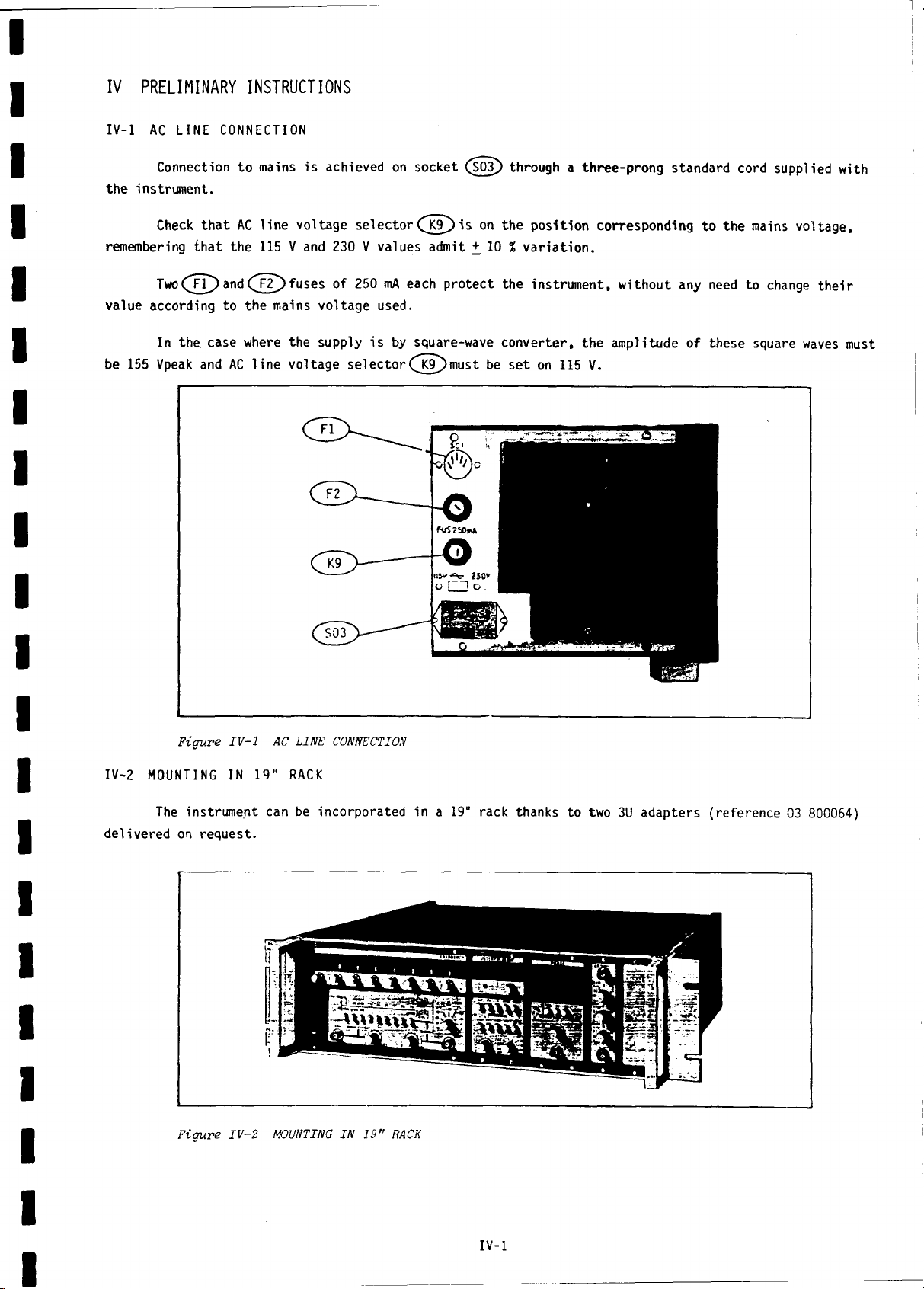
IV-1 AC LINE CONNECTION
Connection to mains is achieved on socket (soT) through a three-prong standard cord supplied with
the instrianent.
Check that AC line voltage se le c to r(^ T)is on the position corresponding to the mains voltage,
remembering that the 115 V and 230 V values admit + 10 % variation.
Two (T T ) andfuses of 250 mA each protect the instrument, without any need to change the ir
value according to the mains voltage used.
In the. case where the supply is by square-wave converter, the amplitude of these square waves must
be 155 Vpeak and AC line voltage s e l e c to r m u s t be set on 115 V.
1
Figure IV-1 AC LINE CONNECTION
IV-2 MOUNTING IN 19" RACK
The instrument can be incorporated in a 19" rack thanks to two 3U adapters (reference 03 800064)
delivered on request.
Figure IV-2 MOUNTING IN 19" HACK
IV-1
Page 18
V OPER ATI NG IN ST RU CT I ON S
V-l EXTERNAL DESCRIPTION
The differe nt controls and connections on the fron t and rear panels o f the 3100B synthesizer and
its options are described on the following plates :
- Plate V -l : fro nt panel of the 3100B
- Plate V-2 : rear panel of the 3100B
- Plate V-3 : programmable attenuator option 311IB
- Plate V-4 : progranmable phase-shifter option 3112B
- Plate V-5 : Search and Sweep option 3114B
V-2 3100B OPERATING INSTRUCTIONS
V-2-1 SWITCHING ON
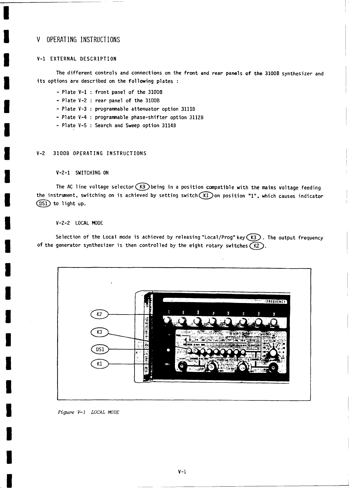
The AC line voltage selectorQ cT)being in a position compatible with the mains voltage feeding
the instrunent, switching on is achieved by setting switch^To^on position "1", which causes indicator
(psT) to light up.
V-2-2 LOCAL MODE
Selection of the Local mode is achieved by releasing "Local/Prog" key . The output frequency
of the generator synthesizer is then controlled by the eight rotary switches Q c T ).
Figure V-l LOCAL MODE
V-l
Page 19
V-2 -3 REMOTE MODE
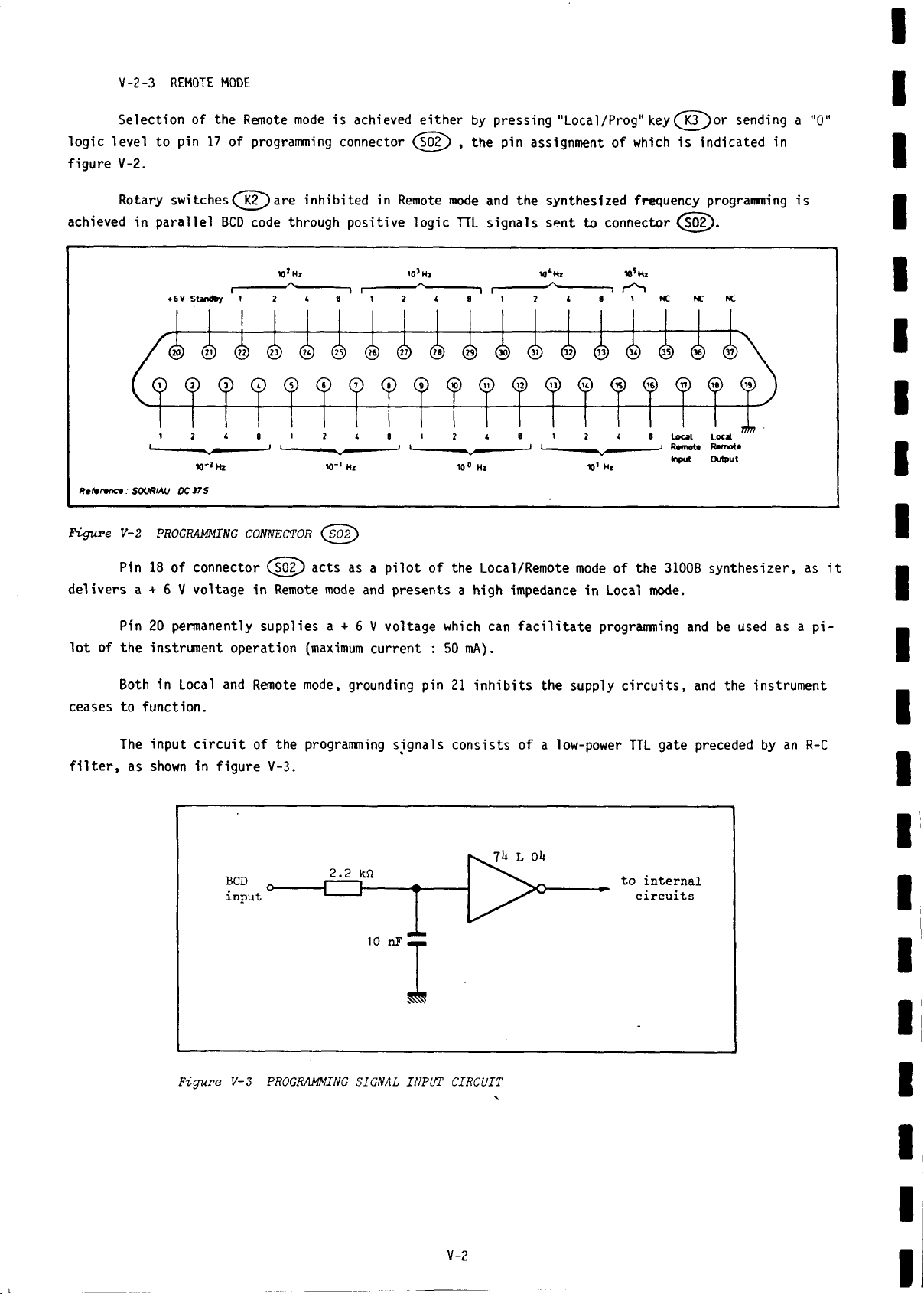
Selection of the Remote mode is achieved either by pressing "Local/Prog" key or sending a "0"
logic level to pin 17 of programming connector (SO?) , the pin assignment of which is indicated in
figure V-2.
Rotary switchesC k2~)are inhibited in Remote mode and the synthesized frequency programming is
achieved in parallel BCD code through positive logic TTL signals sent to connector (S02).
10* Hr 105 Hj K 4« x 10*Hi
46V S t»id by t2t8l248l2*8lNCNCNC
R m fT fK *: SOURIAU OC37S
I I I i I I r n
—^ ^
---
^
Figure V-2 PROGRAMMING CONNECTOR ( S Q 2 )
Pin 18 of connector (SO?) acts as a p ilot of the Local/Remote mode of the 3100B synthesizer, as i t
delivers a + 6 V voltage in Remote mode and presents a high impedance in Local mode.
Pin 20 permanently supplies a + 6 V voltage which can fa c ilita te programming and be used as a p i
lo t of the instrument operation (maximum current : 50 mA).
Both in Local and Remote mode, grounding pin 21 in hib its the supply circuits , and the instrument
ceases to function.
The input c irc u it of the programming signals consists of a low-power TTL gate preceded by an R-C
fil t e r , as shown in figure V-3.
Figure V-3 PROGRAMMING SIGNAL INPUT CIRCUIT
V-2
Page 20
V-2-4 OUTPUT SIGNALS
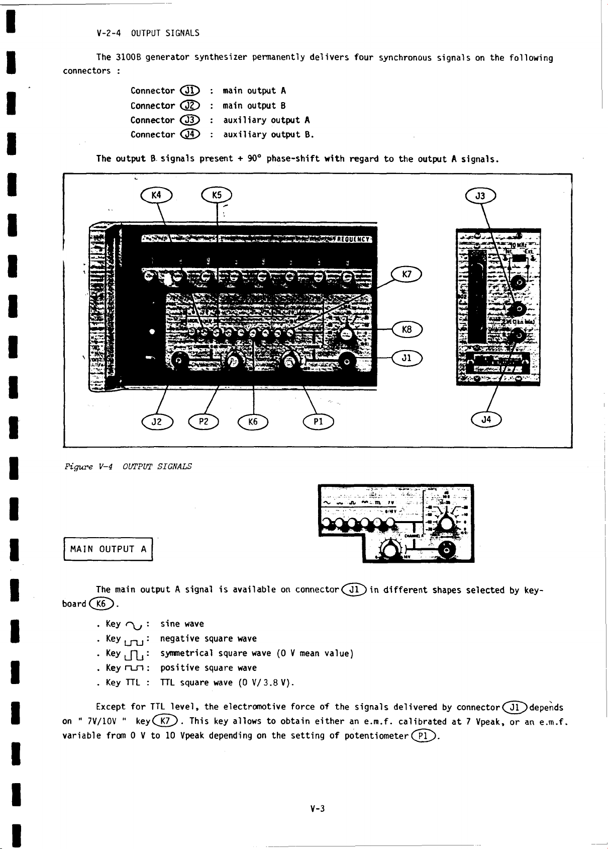
The 3100B generator synthesizer permanently delivers four synchronous signals on the following
connectors :
The output B signals present + 90° phase-shift with regard to the output A signals.
Connector (TT ) : main output A
Connector (3 5 ) : main output B
Connector (3 3 ) : auxiliary output A
Connector (J 4 ) a ux iliary output B.
MAIN OUTPUT A
The main output A signal is available on connector (^ IP ) in d ifferen t shapes selected by key
board .
Key ^
l t d
Key J L
Key n _n
Key TTL
Except fo r TTL leve l, the electromotive force of the signals delivered by connectorC 3 l~ )depends
on " 7V/10V " keyC k7~) . This key allows to obtain eithe r an e.m .f. calibrated at 7 Vpeak, or an e.m .f.
variable from 0 V to 10 Vpeak depending on the setting of potentiometer0 * 0 -
sine wave
negative square wave
symmetrical square wave (0 V mean value)
positive square wave
TTL square wave (0 V /3 .8 V ).
V-3
Page 21
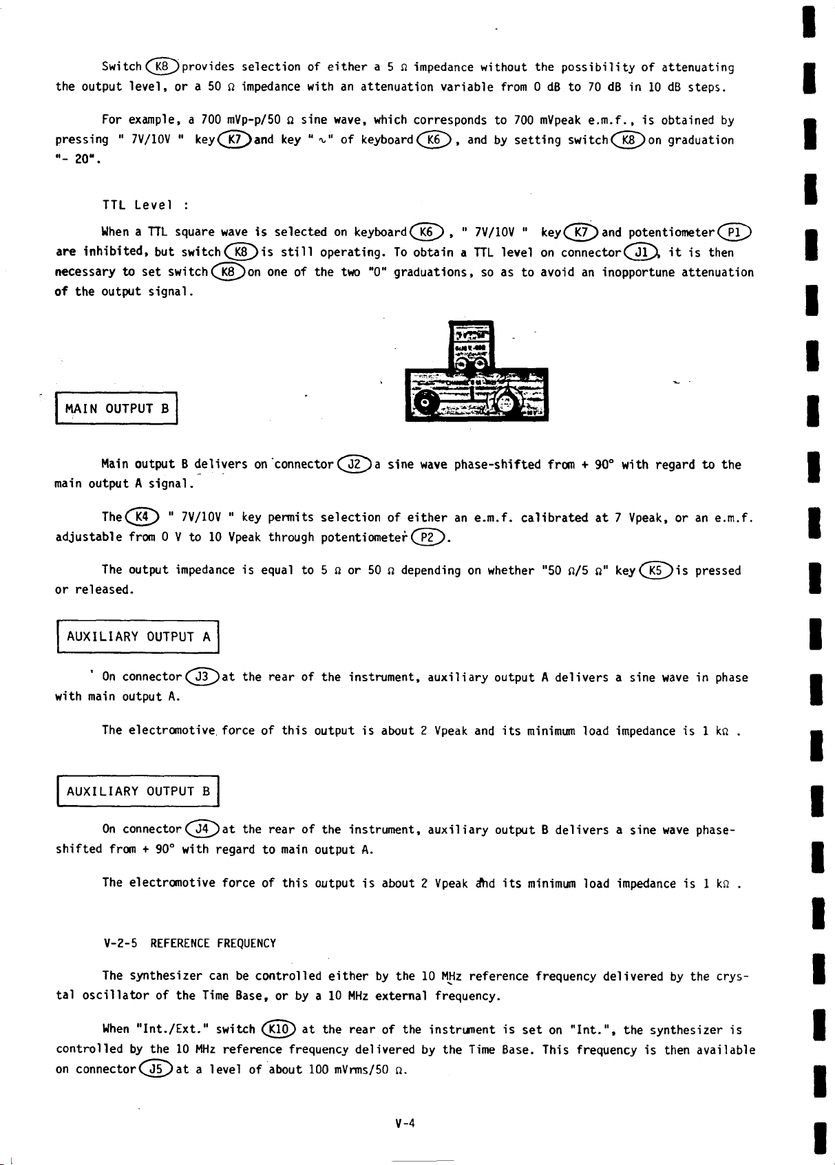
Switch C&P)provides selection of either a 5 S3 impedance without the p o ss ibility of attenuating
the output lev el, or a 50 2 impedance with an attenuation variable from 0 dB to 70 dB in 10 dB steps.
For example, a 700 mVp-p/50 a sine wave, which corresponds to 700 mVpeak e .m .f., is obtained by
pressing " 7V/10V " keyand key “ •x." of keyboard, and by setting swi tch on graduation
20".
TTL Level :
When a TTL square wave is selected on keyboard([wT) , " 7V/10V " key(^K7^and potentiometer(^pT )
are inhib ited, but switch( 'ksP) is s til l operating. To obtain a TTL level on connectorit is then
necessary to set switch(j<jT)on one of the two "0“ graduations, so as to avoid an inopportune attenuation
of the output signal.
MAIN OUTPUT B
Main output B delivers on connectorCJ2^)a sine wave phase-shifted from + 90° with regard to the
main output A signal.
Th e(j<? ) " 7V/10V " key permits selection of eith er an e.m .f. calibrated at 7 Vpeak, or an e.m .f.
adjustable from 0 V to 10 Vpeak through potentiometer (T F ) .
The output impedance is equal to 5 n or 50 n depending on whether "50 fi/5 «" keyCK5~)is pressed
or released.
AUXILIARY OUTPUT A
On connector (^JT) at the rear of the instrument, auxilia ry output A delivers a sine wave in phase
with main output A.
The electromotive, force of this output is about 2 Vpeak and its minimum load impedance is 1 kft .
AUXILIARY OUTPUT B
On connectorat the rear of the instrument, aux iliary output B delivers a sine wave phase-
shifted from + 90° with regard to main output A.
The electromotive force of this output is about 2 Vpeak dhd its minimum load impedance is 1 kn .
V-2-5 REFERENCE FREQUENCY
The synthesizer can be controlled either by the 10 MHz reference frequency delivered by the crys
tal osc illa to r of the Time Base, or by a 10 MHz external frequency.
When "In t./E xt." switch (K ip ) at the rear of the instrunent is set on " In t." , the synthesizer is
controlled by the 10 MHz reference frequency delivered by the Time Base. This frequency is then available
on conne cto rC j?)a t a level of about 100 mVrms/50 a.
V-4
Page 22
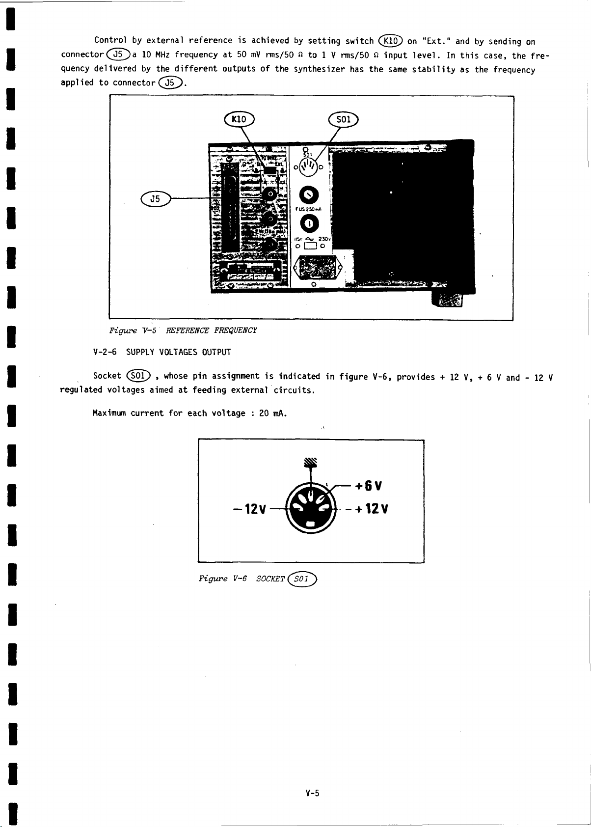
Control by external reference is achieved by setting switch (jclo) on "Ext." and by sending on
co n n ecto r(^[)a 10 MHz frequency at 50 mV rms/50 n to 1 V rms/50 n input level. In this case, the fr e
quency delivered by the d ifferen t outputs of the synthesizer has the same sta b ility as the frequency
applied to connectorC^iP).
Figure V - 5 REFERENCE FREQUENCY
V-2-6 SUPPLY VOLTAGES OUTPUT
Socket (SOI) , whose pin assignment is indicated in fig ure V-6, provides + 12 V, + 6 V and - 12 V
regulated voltages aimed at feeding external circ uits .
Maximum current for each voltage : 20 mA.
V-5
Page 23
V-3 31 1 1 B OP E R AT I NG I N S TR U C T IO N S
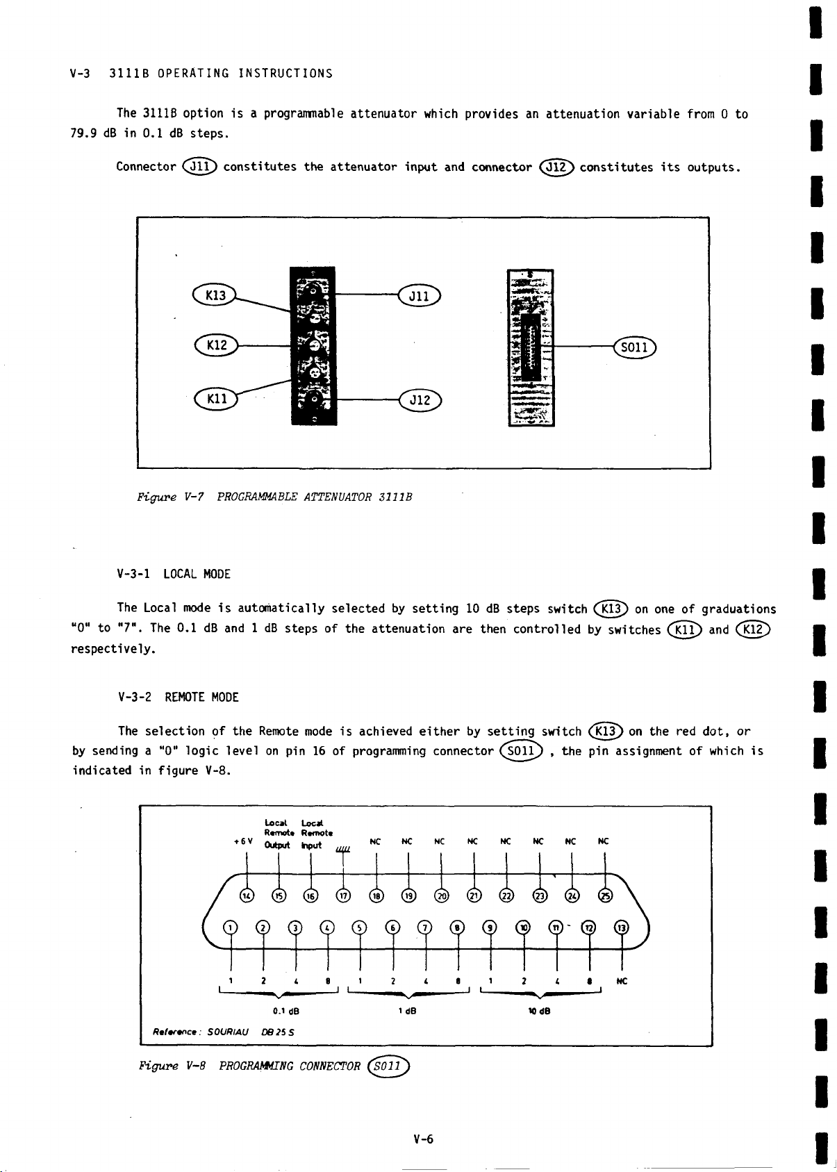
The 3111B option is a programmable attenuator which provides an attenuation variable from 0 to
79.9 dB in 0.1 dB steps.
Connector ( J l Q constitutes the attenuator input and connector (J l? ) constitutes its outputs.
Figure V-7 PROGRAMMABLE ATTENUATOR 3111B
V-3-1 LOCAL MODE
The Local mode is automatically selected by setting 10 dB steps switch (JC13) on one of graduations
“0“ to "7". The 0.1 dB and 1 dB steps of the attenuation are then controlled by switches (jG l) and (K12)
respectively.
V-3-2 REMOTE MODE
The selection pf the Remote mode is achieved eith er by setting switch ( K13) on the red dot, or
by sending a "0" logic level on pin 16 of programming connector ( so il) , the pin assignment of which is
indicated in figure V-8.
Local Local
R tm oU
L
0.1 dB
R tfv tn c * : SOURIAU DB 2S S
Figure V-8 PROGRAmiNG CONNECTOR ( 'SQlT)
1
d B
V
-6
10
48
Page 24
The attenuation programming is achieved in pa rallel BCD code through positive logic TTL signals
sent on connector CsoTT) . As for the programming of the synthesized frequency, the input circ u it of
the programming signals consists of a low-power TTL gate preceded by an R-C fi lt e r (see figure V-3 in
section V-2-3 ).
Pin 15 of connector
SO ll) acts as a p ilo t for the Local/Remote mode of the 3111B programmable
attenuator, as it delivers a + 6 V voltage in Remote mode and presents a high impedance in local mode.
Pin 14 permanently supplies a + 6 V voltage which can fa c ilita te the attenuation programing
(maximum current : 50 mA).
V-4 311 2B OPERATING INSTRUCTIONS
*
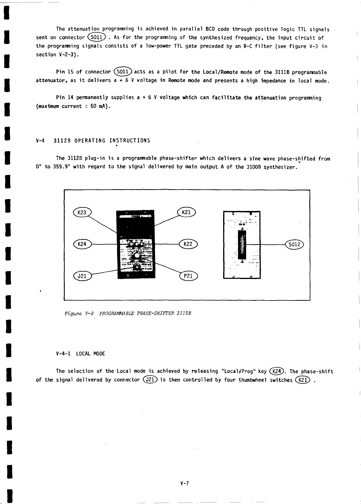
The 3112B plug-in is a programmable phase-shifter which delivers a sine wave phase-shifted from
0° to 359.9° with regard to the signal delivered by main output A of the 3100B synthesizer.
Figure V-9 PROGRAMMABLE PHASE-SHIFTER 3112B
V-4-1 LOCAL MODE
The selection of the Local mode is achieved by releasing "Local/Prog" key (K 24). The phase-shift
of the signal delivered by connector (jf T ) is then controlled by four thumbwheel switches (K 2 l) .
V-7
Page 25
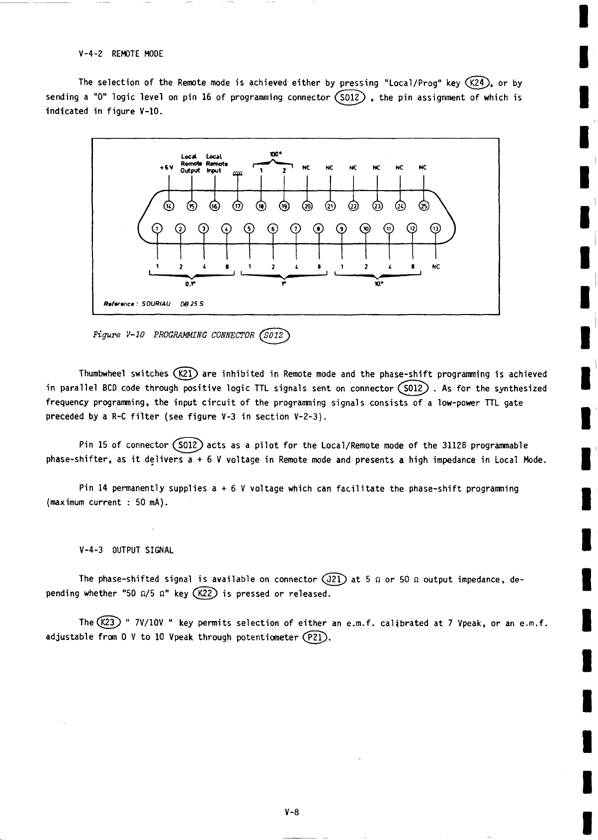
V-4-2 REMOTE MODE
The selection of the Remote mode is achieved eith er by pressing "Local/Prog" key (K24), or by
sending a ”0“ logic level on pin 16 of programming connector ( S0kP) , the pin assignment of which is
indicated in figure V-10.
or
R t / v n n : S O U R IAU D B 2 5 S
Figure V-10 PROGRAMING CONNECTOR CS012
Thumbwheel switches (K2T) are inhibited in Remote mode and the phase-shift programming is achieved
in parallel BCD code through positive logic TTL signals sent on connector ^SOlF) . As for the synthesized
frequency programming, the input circuit of the programming signals consists of a low-power TTL gate
preceded by a R-C fi lte r (see figure V-3 in section V-2-3).
Pin 15 of connector ( S012) acts as a p ilo t for the Local/Remote mode of the 3112B programmable
phase-shifter, as it delivers a + 6 V voltage in Remote mode and presents a high impedance in Local Mode.
Pin 14 permanently supplies a + 6 V voltage which can fa c ilita te the phase-shift programming
(maximum current : 50 mA).
V-4-3 OUTPUT SIGNAL
The phase-shifted signal is available on connector (J2T) a t 5 n or 50 a output impedance, de
pending whether "50 n/5 fi" key ( K2?) is pressed or released.
The ( K23^) " 7V/10V “ key permits selection of either an e.m .f. calibrated at 7 Vpeak, or an e .m .f.
adjustable from 0 V to 10 Vpeak through potentiometer (P2T).
V
-8
Page 26
V-5 3 1 14B OP ER A TI N G I N S T RU C TI O NS
The 3114B Search and Sweep option provides continuous variatio n of the frequency delivered by
the 3100B generator synthesizer and the 3112B programmable phase-shifter. This variation can be achieved
according to four dis tinct modes : Search function, Free-run Sweep, Triggered Sweep, External mode.
V-5 -I SEARCH FUNCTION
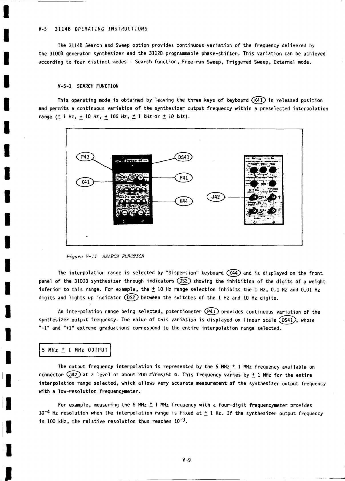
This operating mode is obtained by leaving the three keys of keyboard (K4l) in released position
and permits a continuous variation of the synthesizer output frequency within a preselected interpolation
range (± 1 Hz, + 10 Hz, + 100 Hz, + 1 kHz or + 10 kHz).
Figure V-ll SEARCH FUNCTION
The interpolation range is selected by "Dispersion" keyboard (K44) and is displayed on the front
panel of the 3100B synthesizer through indicators ( PS?) showing the inhibition of the d igits of a weight
infe rio r to this range. For example, the + 10 Hz range selection in hib its the 1 Hz, 0.1 Hz and 0.01 Hz
digits and lights up indicator ( PS?) between the switches of the 1 Hz and 10 Hz dig its.
An interpolation range being selected, potentiometer (P 4l) provides continuous variation of the
synthesizer output frequency. The value of this variation is displayed on lin ea r scale ( DS4T). whose
"-1" and "+1" extreme graduations correspond to the en tire interpo lation range selected.
5 MHz ± 1 MHz OUTPUT
The output frequency interpo lation is represented by the 5 MHz + 1 MHz frequency available on
connector (J4?) at a level of about 200 mVrms/50 a. This frequency varies by + 1 MHz for the entire
interpolation range selected, which allows very accurate measurement of the synthesizer output frequency
with a low-resolution frequencymeter.
For example, measuring the 5 MHz ± 1 MHz frequency with a fo u r-d ig it frequencymeter provides
10-4 Hz resolution when the interp olation range is fixed at ± 1 Hz. If the synthesizer output frequency
is 100 kHz, the re lativ e resolution thus reaches 10‘9.
V-9
Page 27
As the 5 MHz + 1 MHz frequency is generated through arithmetical operations between the frequency
delivered by the interpolation o scillato r and the 10 MHz reference issued from the Time Base, the devia
tion of this 5 MHz + 1 MHz frequency is always exactly proportional to the interpolation of the synthe
sizer output frequency. The proportionality factor varies from 102 for the + 10 kHz range to 10& for the
■» 1 Hz range.
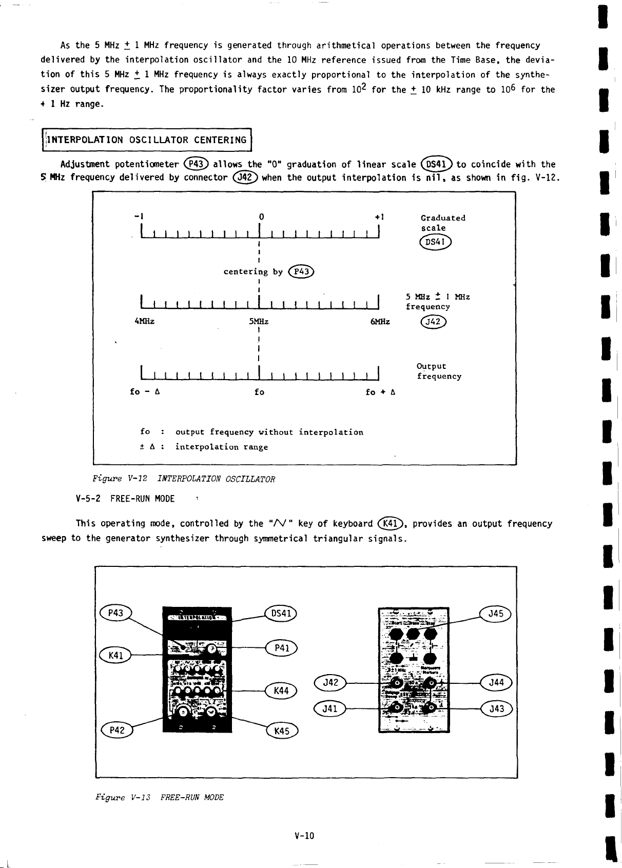
jlNTERPOLATlON OSCILLATOR CENTERING
Adjustment potentiometer (P43) allows the "0" graduation of line ar scale ( DS4l) to coincide with the
5 MHz frequency delivered by connector (J4 2) when the output interpo lation is n il, as shown in fig . V-12.
-1
1 1 I 1 1 1 1 1 1 1 ! 1 1 1 1 1 1 I I
L j
i i i i i I i i 1 i i i i i i i > i 1
L i
AMHz
1 1 1 1 t 1 1 1 1 1 1 1 1 1 1 1 I I 1
u
fo -
A fo fo ♦ A
fo
: output frequency without interpolation
± A
: interpolation range
Figure V-12
INTERPOLATION OSCILLATOR
V-5-2 FREE-RUN MODE
0 +1
\
1
1
centering by ^P43)
I
1
5MHz 6MHz
1
1
1
1
Graduated
scale
X--s
(D S 4 f )
5 MHz t I MHz
frequency
( £ 4 2 )
Output
frequency
This operating mode, controlled by the “A /" key of keyboard (K4p ), provides an output frequency
sweep to the generator synthesizer through symmetrical tria ng ular signals.
Figure V-l 3 FREE-RUN MODE
V-10
Page 28
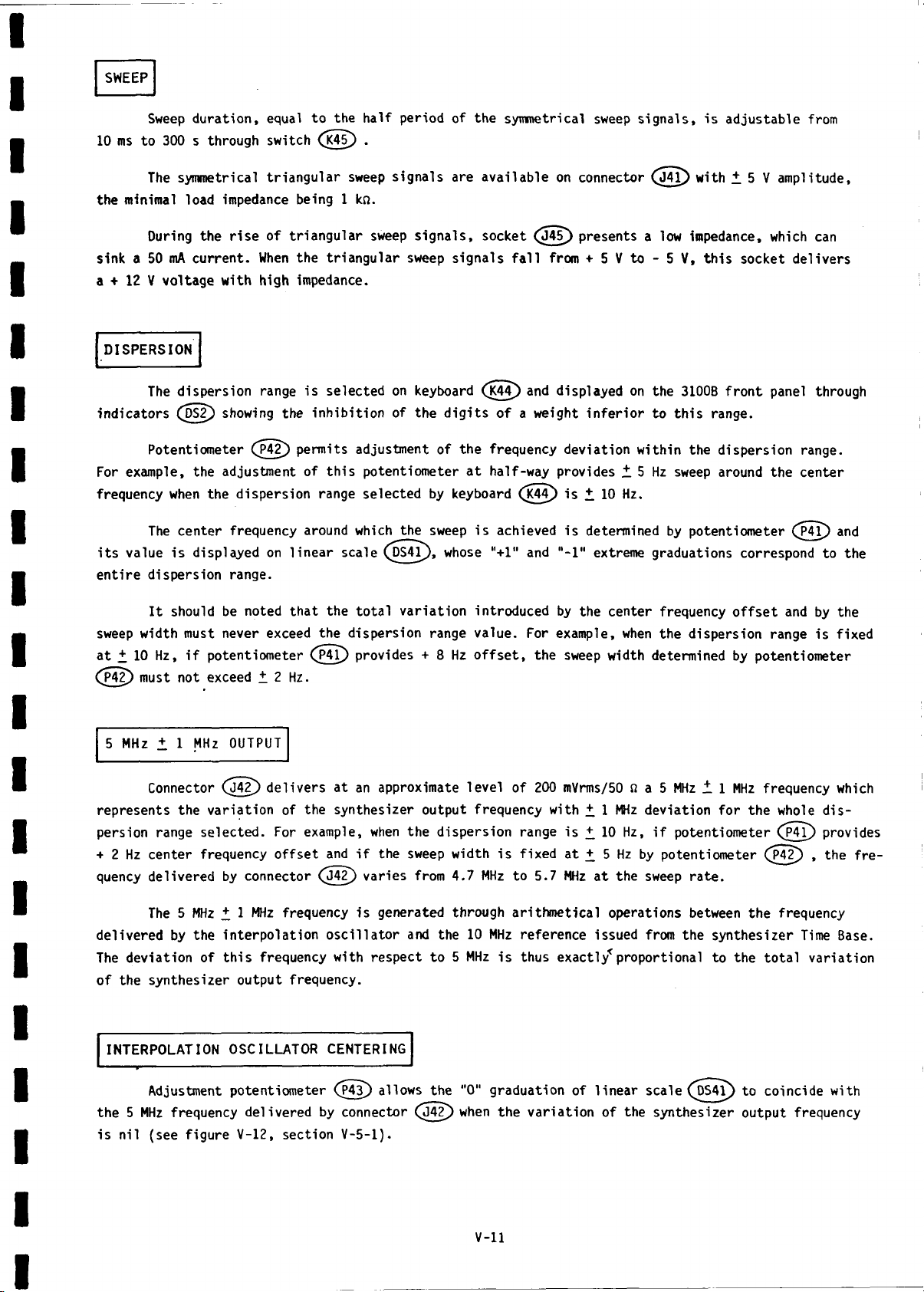
SWEEP
Sweep duration, equal to the half period of the symmetrical sweep signals, is adjustable from
10 ms to 300 s through switch ( K4iP) .
The symmetrical trian gu la r sweep signals are available on connector (J4T) with + 5 V amplitude,
the minimal load impedance being 1 kn.
Ouring the rise of triangular sweep signals, socket (J 4 5) presents a low impedance, which can
sink a 50 mA current. When the triangular sweep signals fa ll from + 5 V to - 5 V, this socket delivers
a + 12 V voltage with high impedance.
DISPERSION
The dispersion range is selected on keyboard (K44) and displayed on the 3100B fro nt panel through
indicators ( DS2) showing the inhibition of the d igits of a weight in ferior to this range.
Potentiometer ( P42) permits adjustment of the frequency deviation within the dispersion range.
For example, the adjustment of this potentiometer at half-way provides ± 5 Hz sweep around the center
frequency when the dispersion range selected by keyboard (K44) is + 10 Hz.
The center frequency around which the sweep is achieved is determined by potentiometer (I mT) and
its value is displayed on line ar scale ( PS4l) , whose "+1" and "-1" extreme graduations correspond to the
entire dispersion range.
It should be noted that the total variatio n introduced by the center frequency o ffset and by the
sweep width must never exceed the dispersion range value. For example, when the dispersion range is fixed
at + 10 Hz, if potentiometer (P4l) provides + 8 Hz o ffs e t, the sweep width determined by potentiometer
(P42) must not exceed i 2 Hz.
5 MHz ± 1 MHz OUTPUT
Connector (J4?) delivers at an approximate level of 200 mVrms/50 II a 5 MHz ± 1 MHz frequency which
represents the variation of the synthesizer output frequency with + 1 MHz deviation for the whole dis
persion range selected. For example, when the dispersion range is i 10 Hz, i f potentiometer (JM~T) provides
+ 2 Hz center frequency offs et and i f the sweep width is fixed at + 5 Hz by potentiometer (P4?) , the fre
quency delivered by connector (J42T) varies from 4.7 MHz to 5.7 MHz at the sweep rate.
The 5 MHz ± 1 MHz frequency is generated through arithm etical operations between the frequency
delivered by the interpolation oscillato r and the 10 MHz reference issued from the synthesizer Time Base.
The deviation of this frequency with respect to 5 MHz is thus exactly'proportional to the total variation
of the synthesizer output frequency.
INTERPOLATION OSCILLATOR CENTERING
Adjustment potentiometer (P4?) allows the "0" graduation of linear scale (J)SaT) to coincide with
the 5 MHz frequency delivered by connector (J4 ?) when the variation of the synthesizer output frequency
is nil (see figure V-12, section V-5 -1 ).
V -ll
Page 29
MARKERS
BIRDY MARKERS
fo - A
fo : center frequency
± A : dispersion range
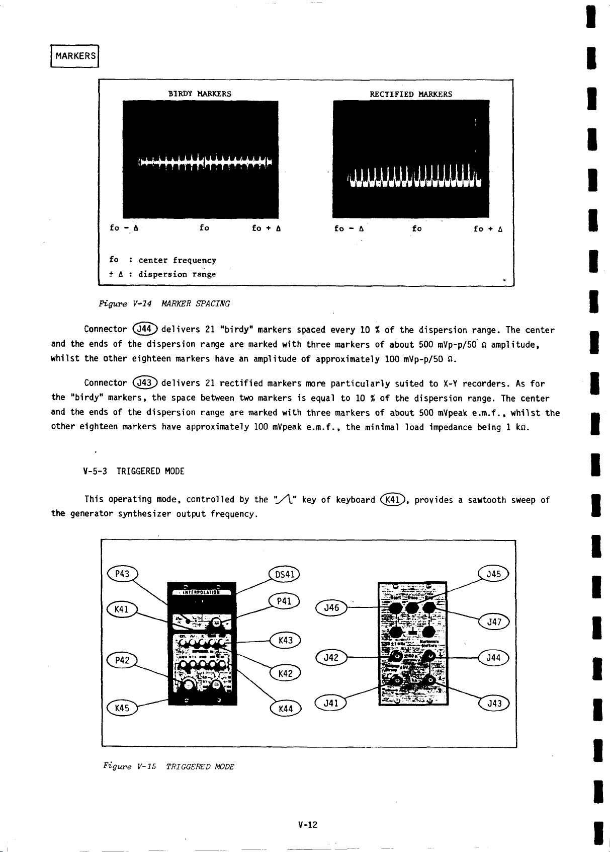
Figure V-14 MARKER SPACING
fo + A
fo - A
RECTIFIED MARKERS
fo
fo + A
Connector ( J44^) delivers 21 “birdy" markers spaced every 10 % of the dispersion range. The center
and the ends of the dispersion range are marked with three markers of about 500 mVp-p/50 « amplitude,
whilst the other eighteen markers have an amplitude of approximately 100 mVp-p/50 n.
Connector ( J43) delivers 21 re ctifie d markers more particu larly suited to X-Y recorders. As fo r
the "birdy" markers, the space between two markers is equal to 10 % of the dispersion range. The center
and the ends of the dispersion range are marked with three markers of about 500 mVpeak e.m .f., whilst the
other eighteen markers have approximately 100 mVpeak e .m .f., the minimal load impedance being 1 kn.
V-5-3 TRIGGERED MODE
This operating mode, controlled by the V ' V key of keyboard (K 4l), provides a sawtooth sweep of
the generator synthesizer output frequency.
V-12
Page 30
SWEEP
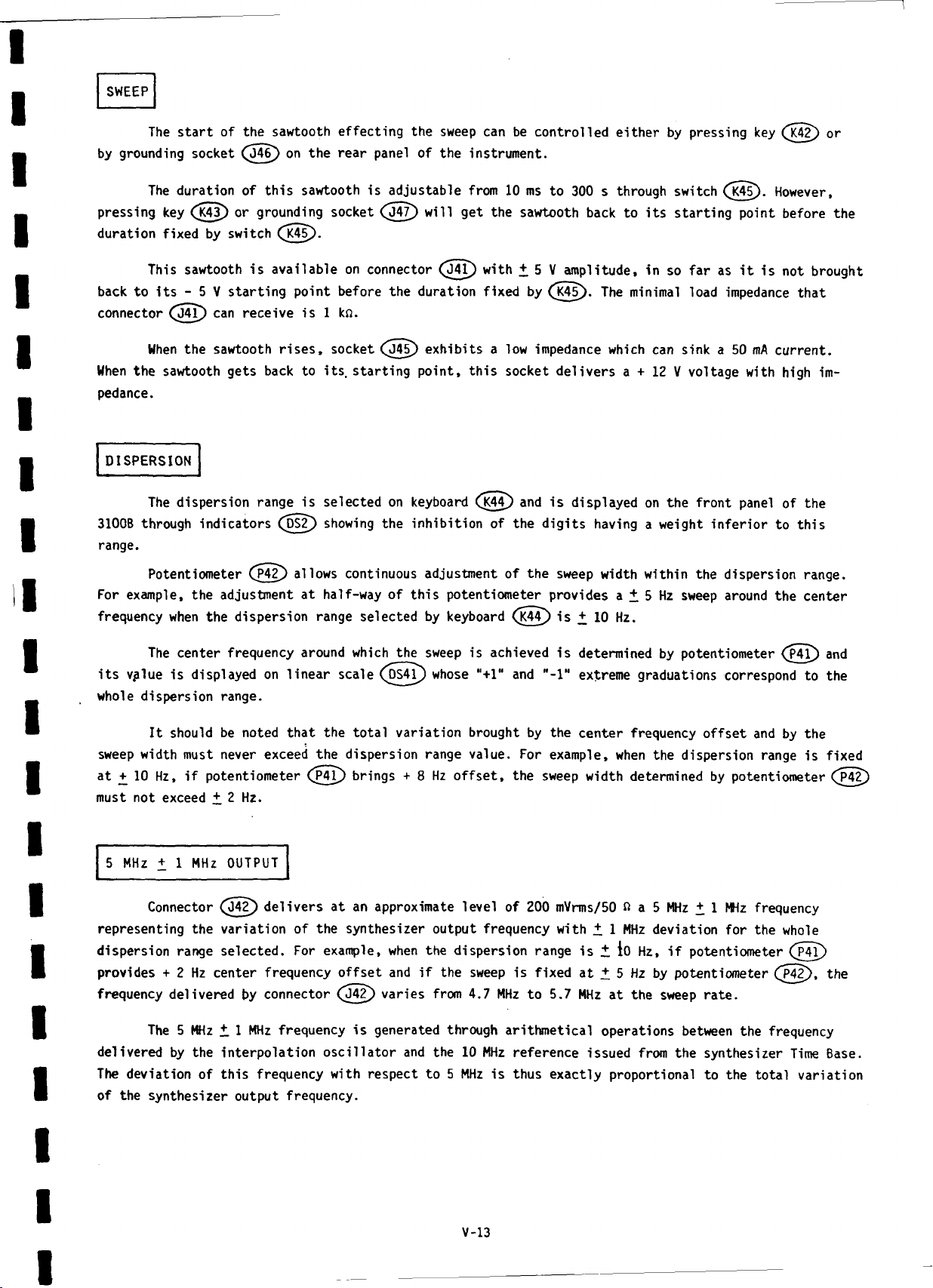
The start of the sawtooth effecting the sweep can be controlled either by pressing key (1(42) or
by grounding socket ( J46) on the rear panel of the instrument.
The duration of this sawtooth is adjustable from 10 ms to 300 s through switch (K45). However,
pressing key (K43) or grounding socket (J47 ) will get the sawtooth back to its starting point before the
duration fixed by switch (K45).
This sawtooth is available on connector (J 4 l) with + 5 V amplitude, in so far as i t is not brought
back to its - 5 V starting point before the duration fixed by (K45). The minimal load impedance that
connector ( J 4 l) can receive is 1 kn.
When the sawtooth ris es, socket (J4 5) exhibits a low impedance which can sink a 50 mA current.
When the sawtooth gets back to its. starting point, this socket delivers a + 12 V voltage with high im
pedance.
DISPERSION
The dispersion range is selected on keyboard (K44) and is displayed on the front panel of the
3100B through indicators (JDS2) showing the inhib ition of the dig its having a weight in fe rior to this
range.
Potentiometer (P42) allows continuous adjustment of the sweep width within the dispersion range.
For example, the adjustment at half-way of this potentiometer provides a + 5 Hz sweep around the center
frequency when the dispersion range selected by keyboard ( K44) is + 10 Hz.
The center frequency around which the sweep is achieved is determined by potentiometer ( P4T) and
its vplue is displayed on line ar scale (jDS4l) whose "+1" and ”-1" extreme graduations correspond to the
whole dispersion range.
It should be noted that the total variation brought by the center frequency o ffset and by the
sweep width must never exceed the dispersion range value. For example, when the dispersion range is fixed
at + 10 Hz, i f potentiometer (P 4T) brings + 8 Hz o ffs et, the sweep width determined by potentiometer (P42)
must not exceed + 2 Hz.
5 MHz + 1 MHz OUTPUT
Connector (0 42 ) delivers at an approximate level of 200 mVrms/50 n a 5 MHz + 1 MHz frequency
representing the variation of the synthesizer output frequency with + 1 MHz deviation for the whole
dispersion range selected. For example, when the dispersion range is ± io Hz, i f potentiometer (P 4l)
provides + 2 Hz center frequency offs et and if the sweep is fixed at ± 5 Hz by potentiometer (P42), the
frequency delivered by connector (J 42) varies from 4.7 MHz to 5.7 MHz a t the sweep rate.
The 5 MHz ± 1 MHz frequency is generated through arithmetical operations between the frequency
delivered by the interpolation os cillator and the 10 MHz reference issued from the synthesizer Time Base.
The deviation of this frequency with respect to 5 MHz is thus exactly proportional to the total variation
of the synthesizer output frequency.
V-13
Page 31

IN TE R P O LATI O N O SC I L L A TO R C E NT E R I N G
Adjustment potentiometer (£43) allows the "0" graduation of lin e a r scale ( dS4T) to coincide w ith
the 5 MHz frequency delivered by connector ( J4?) when the va riation of the synthesizer output frequency
is n il (see fig ure V-12, section V-5-1).
MARKERS
As in free-ru n mode, connectors ( J43) and (J44) respectively d elive r re c tifie d markers and "birdy"
markers spaced every 10 % o f the dispersion range (see section V-5-2).
V-5-4 EXTERNAL MODE
This operating mode con trolled by the "E xt." key of keyboard (K 4 l) makes possible the Search or
Sweep of the synthesizer output frequency by means o f an external sig nal.
Figure V-l 6 EXTERNAL MODE
SWEEP I NPUT
The search or sweep of the synthesizer output frequency is achieved by sending a - 5 V to + 5 V
external voltage on connector (J4T) which, in th is case, presents 10 kfi input impedance.
DISPERSION
The dispersion range is selected on keyboard (K44)and is displayed on the fro nt panel o f the 3100B
through ind icators (DS2) , showing the inh ib itio n o f the dig its having a weight in fe rio r to th is range.
A dispersion range being selected, the frequency variatio n depends both on the amplitude of the
signal applied to connector (J 4 l) and on the position on which potentiometer (P42) is set. To obtain a
frequency variatio n equal to the whole dispersion range, the amplitude of the signal applied to connec
to r ( J4~T) must be + 5 V and potentiometer(P42) must be set on the extreme rig ht p o s ition .
V -1 4
Page 32
5 M Hz + 1 MH z OU T P U T
Connector (J42) delive rs at an approximate level o f 200 mVrms/50 n a 5 MHz ± 1 MHz frequency which
represents the v ariatio n of the synthesizer output frequency with + 1 MHz deviatio n fo r the whole d is
persion range selected.
As the 5 MHz + 1 MHz frequency is generated through arith m etical operations between the frequency
delivered by the interpola tio n os c illa to r and the 10 MHz reference issued from the synthesizer Time Base,
the deviation of th is frequency with respect to 5 MHz is exactly proportional to the v a ria tio n of the
synthesizer output frequency.
INTERPOLATION OSCILLATOR CENTERING ,
S p lit-s h aft potentiometer (P43) permits centering of the in te rpo la tio n o s cilla to r, so th at the
"5 MHz i 1 MHz" output (J42) d e liv ers a 5 MHz frequency when no signal is applied to connector (J 4 l).
MARKERS
As in free-run mode, connectors (J 4 3 ) and (J44) resp ective ly deliver r e ctifie d markers and "b irdy"
markers spaced every 10 % of the dispersion range (see section V-5-2).
V-15
Page 33
VI C IRC UIT D E SCR IPT ION
V I-l INTRODUCTION
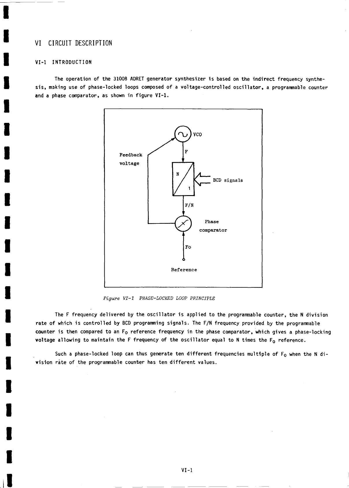
The operation of the 3100B ADRET generator synthesizer is based on the ind irect frequency synthe
sis, making use of phase-locked loops composed of a voltage-controlled oscilla to r, a progranmable counter
and a phase comparator, as shown in figure V I-1.
Feedback
v o lt a g e
Figure VI-1 PHASE-LOCKED LOOP PRINCIPLE
The F frequency delivered by the o scillator is applied to the progranmable counter, the N division
rate of which is controlled by BCD programming signals. The F/N frequency provided by the programmable
counter is then compared to an F0 reference frequency in the phase comparator, which gives a phase-locking
voltage allowing to maintain the F frequency of the o scillator equal to N times the F0 reference.
Such a phase-locked loop can thus generate ten differe nt frequencies m ultiple of F0 when the N di
vision rate of the programmable counter has ten d ifferent values.
VI-1
Page 34

VI-2 C ENT AD E
See block diagram on plate VI-1 and figure VI-2, as well as schematic on plate VI-3.
Figure VI-2 CENTADE
This subassembly elaborates the 10 Hz and 10 Hz increments of the output frequency, by means
of a phase-locked loop consisting of oscillato r 01, progranmable counter DPI and phase-frequency com
parator CPI.
O s cilla to r 01 generates a 19.01 MHz to 20 MHz frequency divided by the N divisio n rate of pro
grammable counter DPI. The frequency delivered by th is counter DPI is then compared in ^hase/frequency
comparator CPI with a 10 kHz reference, obtained by div iding by 10 frequency F9 : 100 kHz issued from
the Time Base. Comparator CPI thus provides a DC voltage phase-locking o sc illa to r 01 to a frequency equal
to N times the 10 kHz reference frequency.
The frequency generated by o sc illa to r 01 is divided by 10 in d ivider 02, then filte re d in band
pass f i l t e r FL1 before being sent to the fir s t Standard Decade.
When an in te rp o la tion range is selected on option 3114B, the + 6 V supply voltage of the Centade
is cut o ff. Besides, i f the interpo la tion range is + 1 Hz, frequency F12 : 2.1 W z/1.9 MHz is sub stituted
at f ilte r FL1 fo r the synthesized frequency (see section VI-11).
-2 -1
VI-2
Page 35
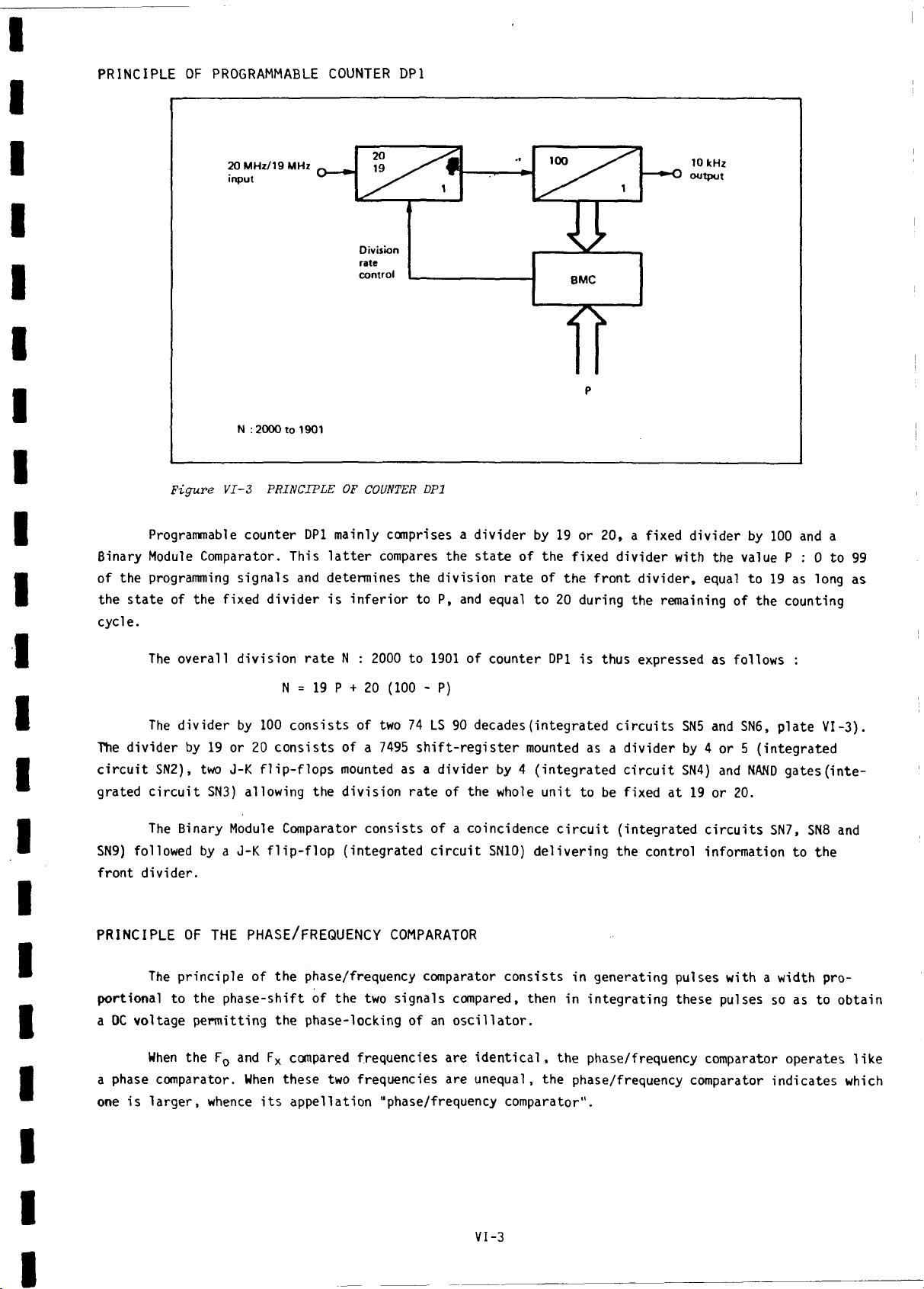
PRINCIPLE OF PROGRAMMABLE COUNTER DPI
N : 2000 to 1901
Figure VI-3 PRINCIPLE OF COUNTER DPI
Programmable counter DPI mainly comprises a divid e r by 19 or 20, a fixe d divider by 100 and a
Binary Module Comparator. This la tte r compares the s tate o f the fixed d iv ider with the value P : 0 to 99
of the programming signals and determines the d ivisio n rate of the fro n t divide r, equal to 19 as long as
the sta te of the fixe d div id e r is in fe rio r to P, and equal to 20 during the remaining o f the counting
cycle.
The overa ll d iv isio n ra te N : 2000 to 1901 of counter DPI is thus expressed as follows :
N = 19 P + 20 (100 - P)
The d ivider by 100 consists of two 74 LS 90 decades(integrated circ u its SN5 and SN6 , plate V I-3 ).
The divider by 19 or 20 consists of a 7495 sh ift-r e gis te r mounted as a divid e r by 4 or 5 (integrated
c ir c u it SN2), two J-K flip -flo p s mounted as a d ivider by 4 (integra ted c irc u it SN4) and NAND gates (in te
grated c irc u it SN3) allo win g the d iv ision rate o f the whole un it to be fixe d at 19 or 20.
The Binary Module Comparator consists of a coincidence c ir c u it (integrated c ircu its SN7, SN8 and
SN9) followed by a J-K flip - flo p (inte gra ted c irc u it SN10) de livering the co ntrol inform ation to the
fro n t d ivid e r.
PRINCIPLE OF THE PHASE/FREQUENCY COMPARATOR
The p rin c iple of the phase/frequency comparator consists in generating pulses with a width pro
portiona l to the phase-shift o f the two signals compared, then in integratin g these pulses so as to obtain
a OC voltage p erm itting the phase-locking of an o s cilla to r.
When the F0 and Fx compared frequencies are id e ntic a l, the phase/frequency comparator operates lik e
a phase comparator. When these two frequencies are unequal, the phase/frequency comparator indicates which
one is larg e r, whence its app ellatio n "phase/frequency comparator".
VI-3
Page 36

As shown in fig ure V I-4, the d ig ita l p art of the phase/frequency comparator consists of two J-K
flip -flo p s , the Q1 and Q2 outputs of which are applied to a NAND gate reacting on the Clear input of
each flip -flo p .
Fx
Fo
Q
Q2
OI
Q
Reset
_ l
1
2
Fx leads Fo
1
• i
11
_ r
- - - -
j - n — r
■TTL
i
- d -
11
Fx lags Fo
1
1
- - - - - - -
T -
-T T L
J ~
_ _ _ _
r
i i _
i
k
JTL
i
t i r
i
-tr 1_r
r
J l
■ T il-
I
1 r
Fx
F i g ur e V I -4 PHASE/FREQUENCY COMPARATOR
■ The Fq and Fx signals to be compared are applied to the CP and J inputs of each flip -flo p . Since
the K inputs are grounded, the negative-going edges of each of the F0 and Fx signals bring about a "1"
lo g ic level on the Q output of the corresponding flip -flo p . On account o f the reactio n of the NAND gate
on the Clear in puts, the Q1 and Q2 outputs return to the "0" state once they have both reached the "1"
sta te , a fte r a short time equal to the propagation time of the NAND gate. In practice, two in te rte rs are
cascaded with the NAND gate, in order to provide a longer propagation time and thereby a larger output
pulse width.
The width differen ce between the pulses delivered by the Q1 and Q2 outputs is thus p roportional
to the phase-shift between the F0 and Fx sign als. A DC voltage proportional to th is phase-shift is then
obtained by integ ra ting the output pulses through the d iffe re n tia l integrator composed of transis tors Q4,
Q5 and Q6 .
Fo
VI-4
Page 37
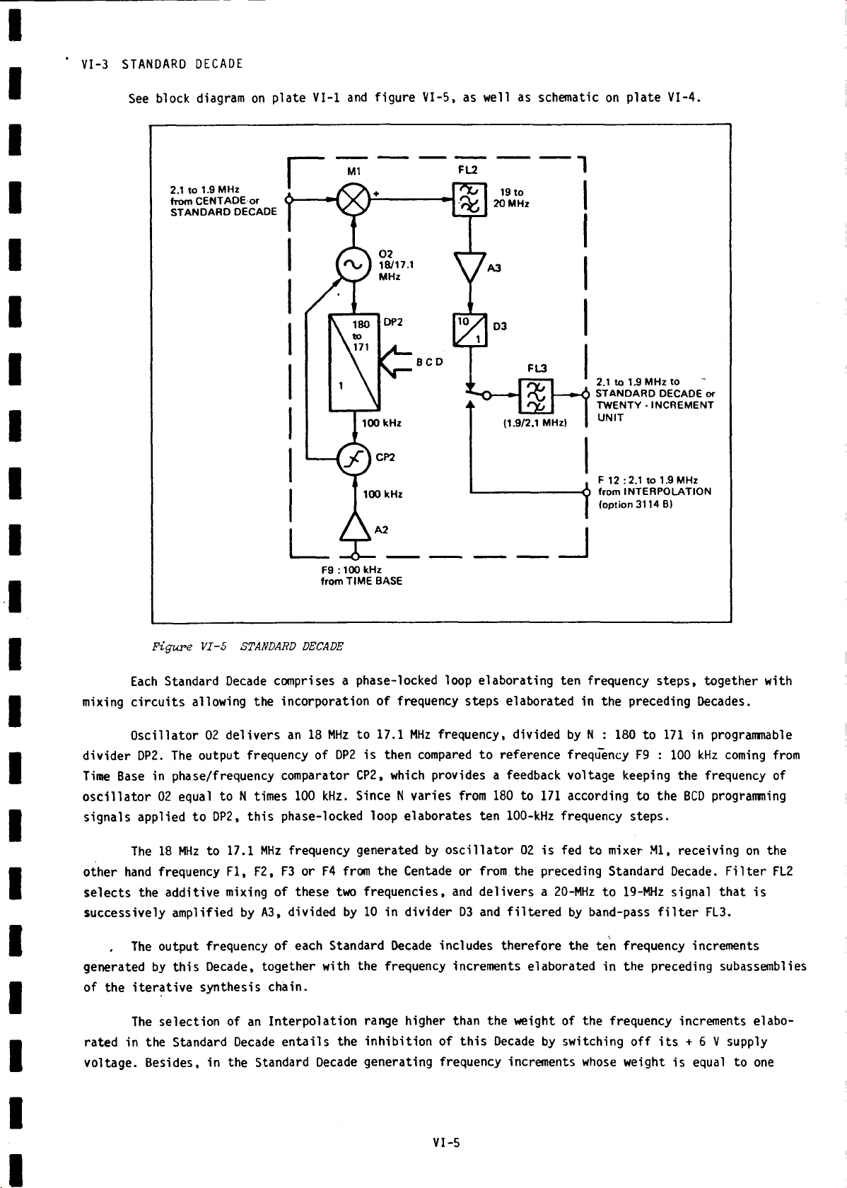
VI-3 S T A ND A RD D E C A D E
See block diagram on plate VI-1 and figure V I-5 , as well as schematic on plate V I-4.
2.1 to 1.9 MHz
from CENTADE or
STANDARD DECADE
2.1 to 15 MHz to
STANDARD DECADE of
TWENTY-INCREMENT
UNIT
F 12 :2.1 to 1.9 MHz
from INTERPOLATION
(option 3114 B)
F9 :100 kHz
from TIME BASE
Figure VI-5 STANDARD DECADE
Each Standard Decade comprises a phase-locked loop elaborating ten frequency steps, together with
mixing circuits allowing the incorporation of frequency steps elaborated in the preceding Decades.
Oscillator 02 delivers an 18 MHz to 17.1 MHz frequency, divided by N : 180 to 171 in progranmable
divider DP2. The output frequency of DP2 is then compared to reference frequency F9 : 100 kHz coming from
Time Base in phase/frequency comparator CP2, which provides a feedback voltage keeping the frequency of
os c illa to r 02 equal to N times 100 kHz. Since N varies from 180 to 171 according to the BCD programing
signals applied to DP2, this phase-locked loop elaborates ten 100-kHz frequency steps.
The 18 MHz to 17.1 MHz frequency generated by os cillator 02 is fed to mixer Ml, receiving on the
other hand frequency F I, F2, F3 or F4 from the Centade or from the preceding Standard Decade. F ilte r FL2
selects the additive mixing of these two frequencies, and delivers a 20-MHz to 19-MHz signal that is
successively amplified by A3, divided by 10 in divider D3 and filte r e d by band-pass fil t e r FL3.
The output frequency of each Standard Decade includes therefore the ten frequency increments
generated by this Decade, together with the frequency increments elaborated in the preceding subassemblies
of the ite ra tiv e synthesis chain.
The selection of an Interpolation range higher than the weight of the frequency increments elabo
rated in the Standard Decade entails the in hibition of this Decade by switching o ff its + 6 V supply
voltage. Besides, in the Standard Decade generating frequency increments whose weight is equal to one
VI -5
Page 38

tenth the Interpo lation range, the synthesized frequency is replaced at f i l t e r FL3 by frequency F12 :
2.1 MHz/1.9 MHz coming from option 3114B (see section VI-11).
For instance, selectin g a + 1 kHz Interp ola tion range causes the in h ib itio n of the f ir s t three
Standard Decades, w hile frequency F12 is substituted for the synthesized frequency in the third Standard
Decade.
PRIN CIPLE OF PROGRAMMABLE COUNTER DP2
N : 180 to 171
Figure VI-6 PRINCIPLE OF COUNTER DP2
The programmable counter DP2 consists essen tially of a divid e r by 17 or 18, a div ider by 10 and
a coincidence c irc u it comparing the state o f the divider by 10 with the value P : 0 to 9 of the BCD
programming signals.
During each counting cycle , th is coincidence c irc u it makes the divisio n rate o f the fro nt divid e r
P times equal to 17 and 10-P times equal to 18. The overall d iv ision rate N may thus be written :
N = 17 P + 18 (10 - P).
The divid e r by 10 consists of a 74 LS 90 decade counter (inte grated c irc u it SN9, p late VI-4).
The coincidence c irc u it is made of three NAND gates (inte grated c ir c u it SN10) decoding" the various
states o f the divide r by 10 acdording to the table of fig ure V I-7, and of four NOR ga,tes detecting the
coincidence between the programming signals and the divide r states decoded by the NAND gates.
For instance, i f a “0" logic level is applied to code inputs 1-2-4 and i t a “1" logic level is
applied to code in pu t 8 , the coincidence c ir c u it detects states 2-3, 4-5-6-7 and 9 of -the div ider by 10.
The fron t divid e r d ivides therefore 7 times by 17 and 3 times by 18 during each coOfiting cycle, which
gives N = 173 as overall div is ion ra te.
VI-6
Page 39
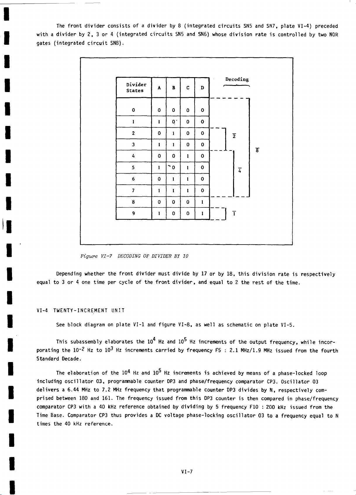
The fro n t d iv id e r consists of a div id er by 8 (inte grate d circ u its SN5 and SN7, plate V I-4) preceded
with a div id e r by 2, 3 or 4 (in tegrated c irc u its SN5 and SN6) whose divisio n rate is c o ntrolled by two NOR
gates (integra ted c irc u it SN8).
Divider
States
0
1 1
2
3 1 1 0 0
4 0 0
5 1 " 0
6
7 I 1 1
8 0 0 0
9 1
A B
0 0
0/
0 ] 0
0 1 1
0
c
0
0 0
1
1
0
Decoding
D
0
0
¥
0
0
0
0
1
1
□
Figure VI-7 DECODING OF DIVIDER BY 10
Depending whether the fro n t d ivid e r must divid e by 17 or by 18, th is divis io n rate is re spectiv ely
equal to 3 or 4 one time per cycle of the fro n t d iv id er, and equal to 2 the rest of the tim e.
VI-4 TWENTY-INCREMENT UNIT
See block diagram on pla te VI-1 and fig u re VI-8 , as w ell as schematic on pla te VI-5.
This subassembly elaborates the 10^ Hz and 10^ Hz increments of the output frequency, while in cor
porating the 10-2 Hz to 103 Hz increments carried by frequency F5 : 2.1 MHz/1.9 MHz issued from the fo urth
Standard Decade.
The ela boration of the 10^ Hz and 10^ Hz increments is achieved by means of a phase-locked loop
including o s cilla to r 03, programmable counter DP3 and phase/frequency comparator CP3. O scilla to r 03
delivers a 6.44 MHz to 7.2 MHz frequency th at programmable counter DP3 divides by N, respe ctively com
prised between 180 and 161. The frequency issued from th is DP3 counter is then compared in phase/frequency
comparator CP3 w ith a 40 kHz reference obtained by div id ing by 5 frequency F10 : 200 kHz issued from the
Time Base. Comparator CP3 thus provides a DC voltage phase-locking o s cilla to r 03 to a frequency equal to N
times the 40 kHz reference.
VI-7
Page 40

The c olle c tion of the 10 Hz to 10 Hz increments carried by frequency F5 and the 10 Hz and
-2 3 4
105 Hz increments of the output frequency is achieved through a second phase-locked loop including
o s cilla to r 04, mixer M2, f i lt e r FL5, a m p lifier A6, divid e r D7 and phase/frequency comparator CP4.
F5 :2.1 to 1.9 MHz F9 : 100 kHz
from STAND ARD DECADE to CENTADE and
Figure VI-8 TWENTY-INCREMENT UNIT
STANDARD DECADES
O s c illator 04 delive rs a frequency variable from 8 MHz to 7.2 MHz that mixer M2 mixes with the
7.2 MHz to 6.44 MHz frequency generated by osc illa to r 03 and filte re d by band-pass f i l t e r FL4. The
substractive beat of these two frequencies is selected by the band-pass filt e r FL5, thus d eliv ering a
840 kHz to 760 kHz frequency. A fte r am plificatio n by A6 and division by 2 in d ivider D7, th is frequency
is applied to phase/frequency comparator CP4, where i t is compared w ith the frequency variable from
420 kHz to 380 kHz obtained by d ividin g by 5 in divid e r D6 frequency F5 : 2.1 MHz/1.9 MHz issued from the
fourth Standard Decade. Thus, comparator CP4 provides a DC voltage which, by means o f the approach voltage
issued from comparator CP3, phase-locks o sc illa to r 04 to a frequency comprising both the increments gener
ated by o s cilla to r 03 and the increments elaborated in the Centade and the Standard Decades.
VI-8
Page 41
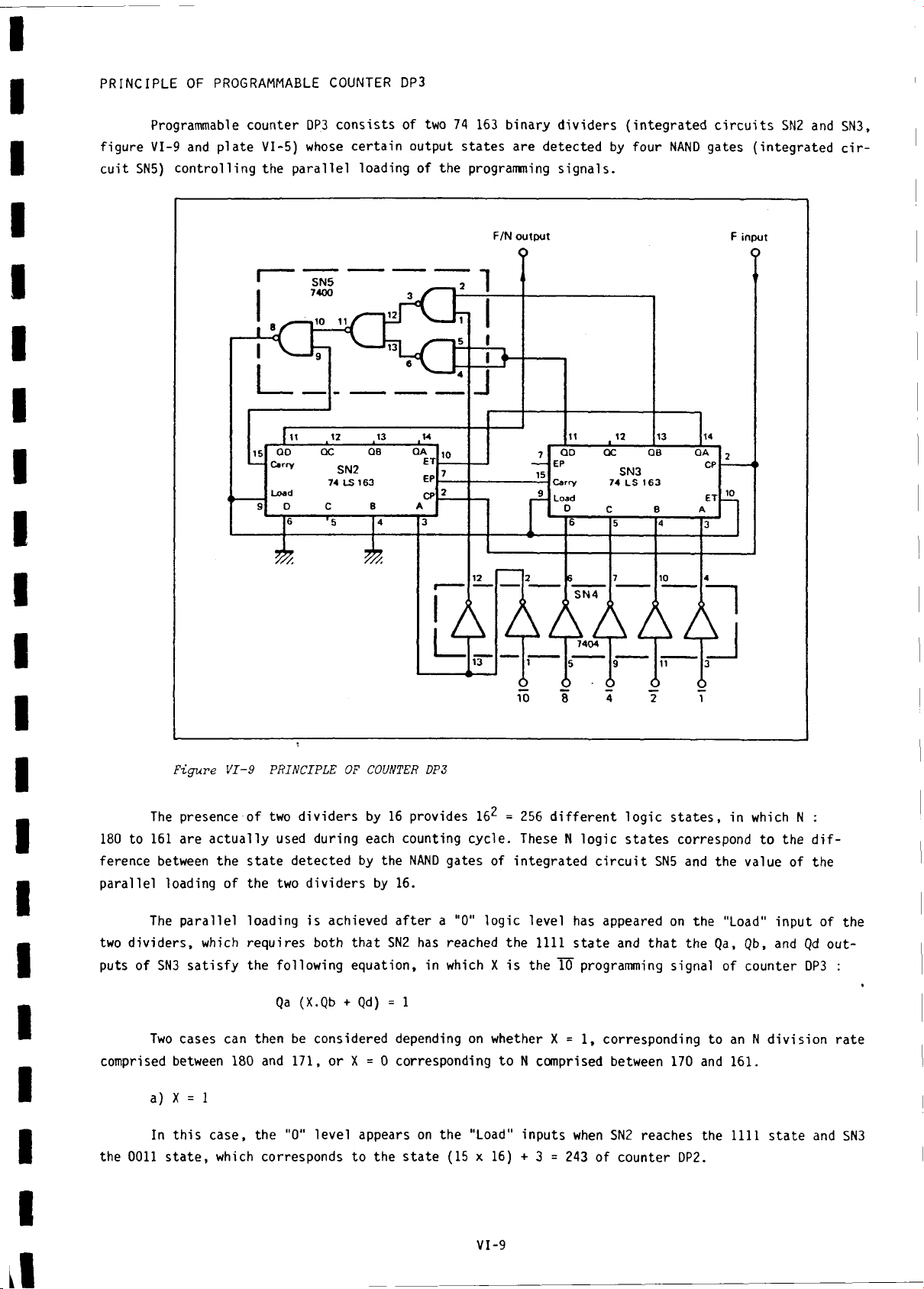
PRINCIPLE OF PROGRAMMABLE COUNTER DP3
Programmable counter DP3 consists of two 74 163 binary divid ers (integ rated c ir c u its SN2 and SN3,
fig u re VI-9 and plate VI-5) whose certa in output states are detected by fo ur NAND gates (integra ted c ir
cu it SN5) c o n trollin g the p a ralle l loading of the programming signals.
F/N output F input
Figure VI-9 PRINCIPLE OF COUNTER DP3
The presence of two d ivid e rs by 16 provides 162 = 256 d iffe re n t logic state s, in which N :
180 to 161 are a ctua lly used during each counting cycle. These N lo g ic states correspond to the d if
ference between the state detected by the NAND gates o f integrated c ir c u it SN5 and the value o f the
para llel loading of the two d ivid e rs by 16.
The paralle l loading is achieved a fte r a "0" lo g ic level has appeared on the "Load" inp ut of the
two divid ers, which requires both th at SN2 has reached the 1111 state and that the Qa, Qb, and Qd out
puts of SN3 satisfy the fo llo w ing equation, in which X is the TO programming signal of counter DP3 :
Qa (X.Qb + Qd) = 1
Two cases can then be considered depending on whether X = 1, corresponding to an N div is io n rate
comprised between 180 and 171, or X = 0 corresponding to N comprised between 170 and 161.
a) X = 1
In this case, the "0" level appears on the "Load" inputs when SN2 reaches the 1111 state and SN3
the 0011 s tate, which corresponds to the state (15 x 16) + 3 = 243 o f counter DP2.
VI-9
Page 42

The pa ra llel loading which occurs at the clock pulse follow ing the appearance o f the "0" level
on the "Load" inputs makes SN2 return to the 0100 state, w hilst SN3 is loaded at the value P : 0 to 9
programmed by the four 1 - 2 - 4- 8 coding signa ls. This p aralle l loading of the two dividers co rres
ponds to the state (4 x 16) + P = 64 + P o f counter DP2.
As the N divisio n rate is equal to the number of states comprises between the 243 fin a l state and
the 64 + P in it ia l state o f the counter, the resu lt is : N = 180 - P.
b) X = 0
In th is case, the "0" level appears on the "Load" inputs when SN2 reaches the 1111 sta te and SN3
the 1011 state, which corresponds to the (15 x 16) + 9 = 249 state of counter DP2.
The p a ra lle l loading which occurs a t the clock pulse followin g the appearance of the "0" level on
the "Load" inputs makes SN2 return to the 0101 state, w hils t SN3 is loaded at the value P : 0 to 9 pro
grammed by the four 1 - 2 - 4 - 8 coding sign als. This paralle l loading o f the two d ividers corresponds
to the (5 x 16) + P = 80 + P state o f counter DP2.
The N div isio n rate, equal to the number of states comprised between the 249 fin al state and the
80 + P in i tia l s tate, becomes in this case : N = 170 - P.
VI-5 OUTPUT MIXER
See block diagram on plate VI-1 and fig ure VI-10, as well as schematic on pla te V I-6 .
F7 :0 to 200 kHz F6 : 8 to 7.2 MHz from F8 : 0 to 200 kHz
channel A TWENTY - INCREMENT U NIT channel B
Figure VI-10 OUTPUT MIXER
This subassembly delivers the output frequency of the synthesizer in the form of two signals in
phase quadrature.
F11 :2 MHz
from TIME BASE
VI-10
Page 43
Frequency F6 : 8 MHz/7.2 MHz issued from the Twenty-Increment unit is amplified by A7, then
divided by 4 in Johnson counter D8, which provides two signals phase-shifted by 90° with a 2 MHz to
1.8 MHz frequency.
Two mixers M3 and M4 mix these signals with frequency F ll : 2 MHz issued from the Time Base,
this frequency being pre-am plified by A8 and filtere d by band-pass fi lte r FL7.
The selection by low-pass fi lte r FL5 of the substractive beat between the signals sent to mixer
M3 provides the F7 output frequency of channel A of the synthesizer. A fter amplification by A9, this
frequency is directed both towards the Function Switch, connectoron the rear panel of the instru
ment and, where applicable, towards option 3112B.
In the same way, low-pass f ilt e r FL6 selects the substractive beat between the signals sent to
mixer M4 and delivers the F8 output frequency of channel B of the synthesizer. A fter amplification by.
A10, this frequency is directed both towards the Function Switch, connector ( [ jT ) and, where applicable,
towards option 3112B.
VI-6 FUNCTION SWITCH
The waveform and the amplitude of the generator synthesizer output signals are determined by the
Function Switch, whose schematic is on plate VI-9.
The F7 sine wave issued from the Output Mixer is , depending on th eC K 6 ^keyboard comnand, changed
into positive,symmetrical or negative square waves through hysteresis comparators SN1 and SN2, or trans
mitted in its original form to the Output Am plifier. In both cases, depending on the position of key(j<7^),
a resistor bridge and potentiometerC pP ) provide a calibrated or continuously variable output level to
main output A.
The F8 sine wave issued from the Output Mixer is always transmitted by the Function Switch without
change of waveform. Depending on the position of k ey pG ^l a resisto r bridge and potentiometer(^pF )
provide a calibrated or continuously variable output level to main output B.
VI-7 OUTPUT AMPLIFIER
The Output Amplifier, the elec trica l diagram of which is on plate VI-7, provides 10 Vpeak e.m .f.
to the signals issued from the Function Switch. This am plification is performed on channels A and B
respectively through two identical amplifiers A ll and A12, each comprising three stages with complemen
tary transistors.
VI-8 TIME BASE
See block diagram on plate VI-1 and figure VI-1 1, as well as schematic on plate VI-8.
The elaboration of the synthesizer output frequency is achieved from a 10 MHz reference, succes
sively divided by 5 in divider D9 and by 10 in divider DIO. These two dividers respectively d eliver fre
quency F ll : 2 MHz aimed at the Output Mixer and frequency aimed at the Twenty-Increment u n it.
When switch (KIO) is on the “Internal" position, th is 10 MHz reference, available on connector(^05^)
at an approximate level of 100 mVrms/50 a, is generated by crystal o scillato r 05.
VI-11
Page 44

When switch (jQ O)is on the "E xternal" po sition, crys tal o sc illa to r 05 is in h ibited and the
frequency synthesis is achieved from an external reference applied to connector
F 13 :10 MHz to
INTERPOLATION F 10 : 200 kHz to
(option 3114 B) TWENTY-INCREMENT UNIT
©
10 MHz Input/Output
Figure VI-11 TIME BASE
VI-9 PROGRAMMABLE ATTENUATOR OPTION 3111B
See block diagram on pla te VI-2 and schematics on pla tes VI-13, VI-14 and VI-15.
The programmable attenuator includes ten w ce lls having the fo llo w ing values : 0.1 dB - 0.2 dB -
0.4 dB - 0.8 dB - 1.6 dB - 3.2 dB - 6.4 dB - 10 dB - 20 dB - 40 dB.
The 10 dB steps of the attenuation are provided by the 10 dB, 20 dB and 40 dB c ells , d ire c tly
co ntrolled in paralle l BCD code.
The 0.1 dB and 1 dB steps of the attenuation are achieved through the 0.1 dB to 6.4 dB c e lls .
These ce lls are c ontro lle d in binary code by two 4008 adders (inte grated circ u its SN1 and SN2, plate
VI-13) performing the BCD/Binary transcoding.
For example, a 14.9 dB attenuation is obtained by v a lidatin g the 10 dB c e ll as well as the 3.2 dB,
1.6 dB and 0.1 dB c e lls .
The p ara llel BCD signals programming the attenuation come e ith e r from the Switch Decoding c ir c u it
(plate VI-14) in Local mode, or from the Code F ilte r (plate VI-15) in Remote mode.
VI-12
Page 45
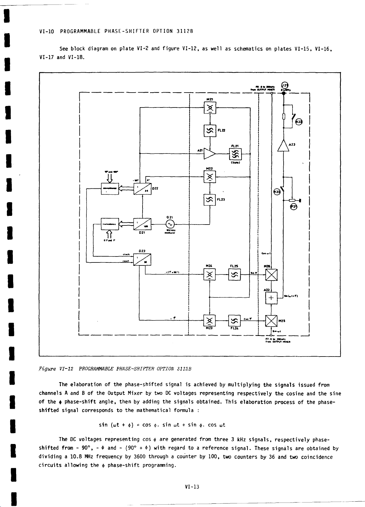
VI-10 PROGRAMMABLE PHASE-SHIFTER OPTION 3112B
See block diagram on pla te VI-2 and figu re VI-12, as well as schematics on plates VI-15, VI-16,
VI-17 and VI-18.
Figure VI-12 PROGRAMMABLE PHASE-SHIFTER OPTION 3112B
The elaboration of the phase-shifted signal is achieved by m ultip lyin g the signals issued from
channels A and B o f the Output Mixer by two DC voltages representing resp ectively the cosine and the sine
of the i phase-sh ift angle, then by adding the signals obtained. This elaboration process o f the phase-
sh ifted signal corresponds to the mathematical formula :
sin (ut + <(>)= cos $. sin wt + sin cos ut
The DC voltages representing cos <f> are generated from three 3 kHz s ign als, resp ective ly phase-
sh ifted from - 90°, - <t> and - (90° + <t>) with regard to a reference signal. These signa ls are obtained by
dividin g a 10.8 MHz frequency by 3600 through a counter by 100, two counters by 36 and two coincidence
c ircu its allow ing the $ pha se-shift programming.
VI-13
Page 46

VI-10-1 DIGITAL PHASE-SHIFT
This subassembly, whose schematic is on plate VI-16, generates the dig ita l signals from which
the DC voltages representing cos $ and sin <j> are elaborated.
The 10.8 MHz frequency that o sc illa to r 021 generates is divided by 100 in counter D21 consisting
of two 74 162 decades (integrated circ uits SN2 and SN3, pla te V I-16). The 108 kHz frequency issued front
counter D21 is divided by 36 in counter D22, which provides both BCD signals perm itting the 10° and 100°
steps programming of the <t> phase-shift and four 3 kHz signals in phase quadrature.
The BCD signals are provided by a div ider by 36, consisting of two 74 162 decades (integrate d c ir
cu its SN4 and SN5) whose synchronous reset is ensured by a NAND gate (in teg rate d circuitySN13) detecting
the state 35 o f the d iv id e r. The signals in phase-quadrature are generated by a Johnson counter con
sis tin g of two J-K flip -flo p s (integrated c irc u its SN15 and SN16) which change state at the same rate as
the divider by 36, so as to d e liver 3 kHz frequency signals.
Counter D21 also provides BCD signals which are applied to a coincidence c irc u it receiving the
programming signals o f the 0.1° and 1 ° steps of the $ phase-shift. This coincidence cir c u it , made up of
exclusive-OR gates (inte gra ted c irc u its SN6 and SN7) whose outputs are linked together so as to co nsti
tute a wired AND, transmits to counter D23 a 108 kHz frequency delayed by the number o f clock pulses
equal to the programmed value o f the 0.1° and 1° steps. Counter D23, which consists o f two d ividers by 3
(integrated c irc u its SN8 and SN9) followed by a Johnson counter(integrated c ir c u it SN10), divides this
frequency by 36 and d e live rs four 3 kHz signals in phase quadrature. A second exclusive-OR coincidence
c irc u it (in tegra ted c irc u its SN11, SN12 and SN14) receiving the BCD signals issued from counter D22 and
the programming signals o f the 10° and 100° steps of the <)> p hase-shift, con trols the reset of this D23
counter, so that its output signals are phase-shifted from $ w ith regard to the signals delivered by
counter D22.
VI-10-2 GENERATION sin <f> / cos $
This subassembly, whose schematic is on plate V I-17, elaborates the DC voltages representing the
cosine and the sine of the <f> pha se-shift angle.
The signal phase-shifted from - 90° that counter D22 de livers is made sinusoidal by band-pass
f ilt e r FL21 preceded w ith am plifie r A21. The gain o f th is am plifier is regulated through a synchronous
detection performed by mixer M21 followed by low-pass f il t e r FL22, which provides a constant level to the
sine wave delivered by filt e r FL21.
On the other hand, mixer M22 followed by low-pass fi l t e r FL23 achieves a phase detection between
th is sinusoidal signal and the 0° reference signal delivered by counter D22. Thus, low-pass filte r FL23
provides a DC voltage phase-locking o sc illa to r 021 to the frequency fo r which band-pass f i l t e r FL21
brings no phase-sh ift.
Mixer M23 performs the frequency beat between the sine wave delivered by f ilt e r FL21 and the signal
phase-shifted by -$ issued from counter D23, which provides at the output of low-pass f i lt e r FL24 a DC
voltage representing cos <f>.
In the same way, mixer M24 performs the frequency beat between the sine wave delivered by fi l t e r
FL21 and the signal phase-shifted by - (90° + 41) issued from counter D23, so as to obtain at the output
of low-pass filt e r FL25 a DC voltage representing sin <f>.
VI-14
Page 47
VI-10-3 OUTPUT CIRCUIT
This subassembly, whose schematic is on plate VI-18, delivers the sin (ut + $) output s ign al by
m ultip lying the sine waves issued from channels A and B of the Output Mixer by the two DC voltages
generated in the preceding subassembly. Linear m ultip lie r M25 rea lizes the product between the voltage
representing cos $ and the F7 signal issued fro * the Output Mixer, whilst the product between the voltage
representing sin <t> and the F8 signal Issued from the Output Mixer 1s carried out by lin e a r m u ltip lie r M26.
The cos $. sin ut and sin $. cos u t signals respectively delivered by M25 and M26 are sunrted up in
current adder A22, which thereby provides a sine wave phase-shifted from t with regard to the signal of
channel A of the synthesizer. The level of th is phase-shifted signal is adjusted by potentiometer (P?T)
or calibrated by a resis to r bridge, then am plified by A23 which de liv ers to output connector (J2T) up to
10 Vpeak electrom otive force.
V I-U SEARCH AND SWEEP OPTION 3114B
See block diagram on plate VI-2 and fig ure VI-13, as well as schematics on plates VI-19 and VI-20.
VI-15
Page 48

The Search and Sweep option delivers frequency F12 : 2.1 MHz/1.9 MHz which, su bstituted fo r one
of the FI to F5 frequencies synthesized by the Centade and the Standard Decades, provides a continuous
va riatio n of the synthesizer output frequency. Moreover, twenty-one markers obtained by beat between th
frequency generated by the interpola tio n oscillator and a 100 kHz frequency d ire ctly derived from refer
ence frequency F13 : 10 MHz issued from the Time Rase, allow use of the 3100B 3114B unit as a sweeper
VI-11-1 SWEEP
This subassembly, whose schematic is on plate VI-19, delivers the signal c o n tro lling the frequent
of in te rp o latio n o s c illa to r 041 according to the operating mode selected on keyboard (K4~T).
- In Search mode, the frequency of oscillato r 041 is adjusted through potentiometer (P 4 l).
- In External mode, th is frequency is controlled by the voltage applied to connector ( J41~) . pos
sibly attenuated by potentiometer (?42).
- In Free-run mode, h ysteresis comparator A43 and integrator A42 d e live r symmetrical tria n g les
ensuring the sweeping o f o sc illa to r 041. The duration of these tria n gles is determined through a res isto
network switched by (K 45) so as to f ix the sweep duration between 10 ms and 300 s. The amplitude control
of these triangle s achieved by potentiometer (P42)allows adjustment o f the sweep width, while the super
po sition of a DC voltage determined by potentiometer (^P4~T) provides continuous adjustment of the center
frequency around which the sweep is achieved.
- In Triggered mode, the frequency o f o s c illa to r 041 is swept by a sawtooth generated through
hysteresis comparator A43 and integrator A42, changed in to a one-shot circ u it by the R-S flip -flo p . This
flip - flo p delivers at the end of each sawtooth a "0* logic level which brings the hysteresis comparator
back to its origin al state. Pressing 'Stop* key ( M 3 ) or applying a *0" level to socket (j4 7 )a lso cause
the appearance of this "0* level on the R-S flip -flo p , which w ill not disappear until "Start" key (K42)
is pressed or u n til a "0" level is applied to socket (J46) . As 1n free-run mode, the sweep duration is
determined by switch (M S ) , the sweep width is adjusted by potentiometer ( P42) , w h ilst potentiom eter
(pTT) provides continuous adjustment of the center frequency.
VI-11-2 INTERPOLATION
This subassembly, whose schematic is on plate VI-20, de livers frequency F12 : 2.1 MHz/1.9 MHz as
well as the m»rkers and the 5 (Hz * 1 MHz frequency representing the output frequency va riation of the
generator synthesizer.
Oscillator 041 generates a frequency variable from 21 MHz to 19 MHz, from which frequency F12:
2.1 MHz/1.9 Wiz is directly derived through a division by 10 in divider D43 . This osc illator is con
trolled through linearity corrector A41 by the control voltage delivered by the Sweep subassembly.
Mixer M4 and band-pass fi lt e r FL43 make a substractive beat between the frequency of os cillato r 04
previously filtere d by band-pass f ilt e r FL41, and a 25 MHz frequency delivered by band-pass f ilt e r FL42.
As this 25 MHz frequency 1s d irectly derived from frequency F13 : 10 MHz through division by 2 and har
monic selection, the substractive beat selected by fi lt e r FL43 provides a 5 MHz * 1 MHz frequency whose
variation represents exactly the variation of the synthesizer output frequency.
Reference frequency F13 : 10 MHz Issued from the Time Base is divided by 100 in dividers D41 and
D42, the outputs of which are linked to a NAND gate pulse generator delivering both 100 kHz frequency
pulses and 1 MHz frequency pulses having an amplitude double that of the f ir s t ones. These pulses are
applied to sampler M42, receiving on the other hand, the 21 MHz/19 MHz frequency generated by
VI-16
Page 49
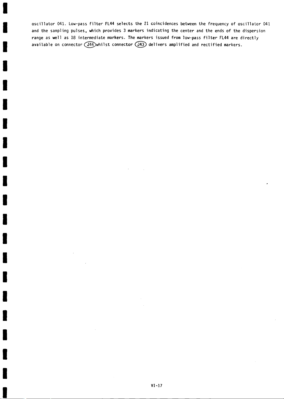
o s cilla to r 041. Low-pass fil t e r FL44 selects the 21 coincidences between the frequency o f o scilla to r 041
and the sampling pulses, which provides 3 markers indic atin g the center and the ends of the dispersion
range as well as 18 intermediate markers. The markers issued from low-pass f i lt e r FL44 are d ire ctly
av aila ble on connector ^J4?)whi 1st connector (J43) delivers am plified and re c tifie d markers.
VI -17
Page 50

a d r e t [ g l i a d f c r io r i iq p G J w
OPTION IEEE BUS OPERATING INSTRUCTIONS
This option made of two boards tr anslates the IEEE bus information into
parallel BCD signals. It su bstitutes in programming to the local synthesizer
controls.
The board connecte ur isolate the IEEE bus signals from those of the
inst rument.
The board bus carri es the exchange protocol of the IEEE bus, the address
recognition, the Loca l/Remote control and the five registers decoding. Four
of the m, nam ely A, B, C and D are used by the wired options of the
instrument (3111 and 3112), and the fifth register is reserved to the fr e
quency program mation.
Both option 3111 and 3112 can be pro grammed by either registers A, B, C
or D. *
The frequency is programmed by hundredths of a Hz steps.
The phase shift is programmed by tens of a degree steps.
The att enuat ion is programmed in tens of a dB steps.
The message is enabled by a ca rriage return (RC) a question mark (?) or a
end of message trigger.
Functions : AH1, T0, SH0, LE0, SR0, RL2, TE0, Ll, PP0, DCl, DTI, C0.
f . D F D C
®
0 C B A
©
* Definition of the programming prefix corresponding to the wired option.
VI-18
Page 51
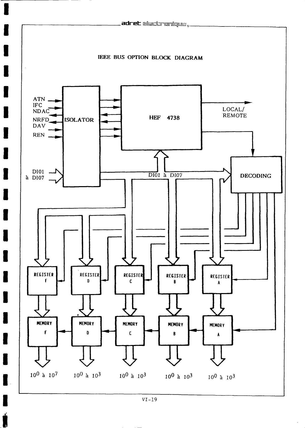
______
IEEE BUS OPTION BLOCK DIAGRAM
adret BEOiacfcirniraoiqpii! &
____
VI-19
Page 52

HP 8 5
a dd r es s
HP 9 8 2 5 ad dr e s s 0
PET a d d r e s s 4
a ) p h a se
sw ee p
B A
b ) l e ve l
sw ee p
c ) f r e q u e n c y
V I - 2 0
sw ee p
10 OUTPUT 7 0 0 ; "
20 FOR X = 0 t o 3 50 0 STEP 10
30 OUTPUT 7 0 0 ; " B " , X
40 NEXT X
50 GOTO 20
10 OUTPUT 7 0 0 ; " F 1 0 0 0 0 0B 1 0 0 "
20 FOR X = 0 t o 5 0 0 STEP 10
30 OUTPUT 7 0 0 ; " A " , X
40 NEXT X
50 GOTO 20
10 OI SP "S ta r t f re q u e n c y "
OI N PUT F
20 DI SP " S t o p f r e q u e n c y "
© I N P U T X
30 OUTPUT 7 0 0 ; " A 0 "
40 FOR J r F t o X STEP 10
50 OUTPUT 7 00 ; " F ", J
60 NEXT J
70 GOTO 10
0 w r t 7 0 0 . "F
1 f o r X = 0 t o 3 5 00 b y 10
2 w r t 7 0 0 . " B " . X
3 n e xt X
4 g t o 1
0 w r t 7 0 0 . "F
1 f o r X = 0 t o 50 0 b y 10
2 w r t 7 0 0 . " A " , X
3 n e x t X
4 g t o 1
0 e n f ' S t a r t fre q u e nc y " , F
1 e n t " S to p f r e qu e nc y " , X
2 w r t 7 0 0 . " A 0 "
3 f o r J = F t o X by 10
4 w r t 7 0 0 , " F " . J
5
ne x t
J
6 g to 0
10 OPEN 1 . 4
20 PRIN T « 1 . " F 1 0 0 0 00 A 0 ”
30 FOR X = 0 t o 35 0 0 STEP
<*0 PR INT # 1 . " B " . X
50 NEXT X
60 GOTO 30
10 OPEN 1 . 4
20 PR INT t 1 . " f
30 FOR X = 0 t o 5 0 0 STEP 10
40 PR INT « . " A " . X
50 NEXT X
60 GOTO 30
10 OPEN 1 , 4
20 P R I N T " S ta r t f r e q u e n c y " :
INPU T F
30 P R I N T " S t o p f r e q u e n cy " : INPUT X
40 P RINT * 1 . " A 0 "
50 FOR J = F t o X STEP 10
60 PR INT # 1 , " F " . J
70 NEXT J
80 GOTO 2 0
©
a d r e t igOiSEfcriraniDiqiiLQi:
ITiSl
p 0 C B A
c\j r- r- r-
d ) p ha s e
t h a n
l e v e l
sw eep
10 D IS P " F r e q ue n cy " fe i I N P U T F
20 OUTPUT 7 0 0 ; " A 0 F " , F
30 FOR X = 0 t o 3 50 0 STEP 10
40 OUTPUT 70 0 ; " D " . X
50 NEXT X
60 FOR X = 0 t o 50 0 STEP 10
70 OUTPUT 7 0 0 ; "A " , X. "B " .
X, "C " , X
80 NEXT X
90 GOTO 10
0 e n t " F r e q u en c y " . F
1 w r t 7 0 0 . " A 0F" . F
2 fo r X = 0 t o 3 5 00 by 10
3 wr t 7 0 0 , " 0 " . X
4 n ex t X
.5 f o r X = 0 t o 50 0 by 10
6 w r t 7 0 0 . " A " . X. " B " . X.
" C ". X
7 nex t X
8 g t o 0
10 OPEN 1. 4
20 P RI N T " F r e q ue nc y” : INPUT F
30 PRI NT * 1 . "A 0 F " . F
40 FOR X = 0 t o 3 50 0 STEP 10
50 PRI NT # 1 . " D " . X
60 NEXT X
70 FOR X = 0 t o 50 0 STEP 10
80 PR INT * 1. " A " . X. " B " . X,
" C " . X
90 NEXT X
100 GOTO 20
Page 53
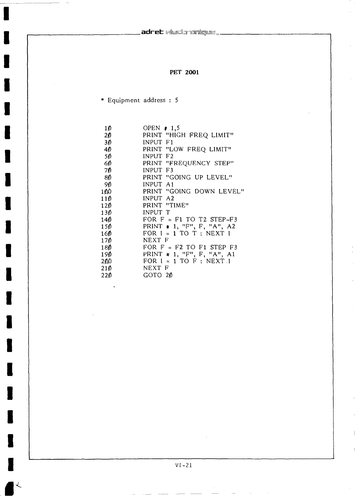
a d r e t i f f i U iM e lb r la r fi m iu iiiJ „
PET 2001
* Equipment address : 5
10 OPEN # 1,5
20 PRINT "HIGH FREQ LIMIT"
30 INPUT FI
40 PRINT "LOW FREQ LIMIT"
50 INPUT F2
60 PRINT "FREQUENCY STEP"
70 INPUT F3
80 PRINT "GOING UP LEVEL"
90 IN PU T A l
10/) PRINT "GOING DOWN LEVEL"
110 INPUT A2
120 PRINT "TIME"
130 INPUT T
140 FOR F = FI TO T2 STEP-F 3
150 PRINT # 1, "F", F, "A", A2
160 FOR I * 1 TO T : NEXT I
170 NEXT F
180 FOR F = F2 TO F I STEP F3
190 PRINT « 1, "F", F, "A", Al
20/) FOR I = 1 TO F : NEXT.I
210 NEXT F
220 GOTO 20
VI-21
 Loading...