

ADMTK AN983BL, AN983B Datasheet

AN983B/AN983BL
PCI/miniPCI-to-Ethernet LAN
Controller
DATASHEET
Rev. 1.8
MAY. 2003
ADMtek.com.tw
Information in this document is provided in connection with ADMtek products. ADMtek may make changes to specifications
and product descriptions at any time, without notice. Designers must not rely on the absence or character istics of any features
or instructions marked "reserved" or "undefined." ADMtek reserves these for future definition and shall have no responsibility
whatsoever for conflicts or incompatibilities arising from future changes to them.
The products may contain design defects or errors known as errata, which may cause the product to deviate from published
specifications. Current characterized errata are available on request. To obtain latest documents, please contact your local
ADMtek sales office or your distributor or visit ADMtek’s website at http://www.ADMtek.com.tw
*Third-party brands and names are the property of their respective owners.

AN983B PCI/miPCI Fast Ethernet Controller with integrated PHY
Datasheet Revision History
Revision Date Revision Description
Oct, 2000
0.1 Draft data sheet for review
Feb, 2001
1.0 First release
Mar, 2001
1.1 Add CSR15.bit28 MRXCK
Add CSR18.bit26 PMEP
Add CSR18.bit27 PMEPEN
Sep, 2001
1.2 Add 25MHz crystal accuracy
Revise PHY registers
Sep, 2001
1.3 Revise product logo of Pin assignment diagram
Sep, 2001
1.4 P.17 MrxD0~D3
P.23 CIOSA : 1 means enable ; 0 means disable
P.14 Add LED info to pin diagram
JULY, 2002
1.5 P.25 Offset 80h, DID default value : 0981h
P.40 CSR18[25] / PWRS_clr : 1 means PCI_reset rising will clear
CR49[1:0]/PWRS
JULY, 2002
1.6 P.85 FIG21, FIG22, FIG23, FIG24 added for MII interface signal
timing.
JULY, 2002
1.7 P.45 Unicast registers added
MAY, 2003
1.8 P.69 Modify some error statement about Loop-back Operation of
transceiver
Table- 1 Revision History
ADMtek Inc.
www.admtek.com.tw
Rev. 1.8
2

AN983B PCI/miPCI Fast Ethernet Controller with integrated PHY
CONTENTS
Datasheet Revision History................................................................................. 2
1. GENERAL DESCRIPTIONS...................................................................................... 9
2. SYSTEM BLOCK DIAGRAM.................................................................................. 10
3. FEATURES................................................................................................................. 11
INDUSTRY STANDARD ............................................................................................ 11
FIFO...................................................................................................................... 11
PCI I/F................................................................................................................... 11
EEPROM/BOOT ROM I/F .................................................................................... 11
MAC/PHYSICAL .................................................................................................... 12
LED DISPLAY........................................................................................................ 12
MISCELLANEOUS ................................................................................................... 12
4. BLOCK DIAGRAM................................................................................................... 13
5. PIN ASSIGNMENT DIAGRAM............................................................................... 14
6. PIN DESCRIPTION................................................................................................... 15
7. REGISTERS AND DESCRIPTORS DESCRIPTION............................................ 19
7.1 AN983B configuration registers......................................................................... 20
7.1.1. AN983B configuration registers list....................................................... 20
7.1.2. AN983B configuration registers table.................................................... 21
7.1.3 AN983B configuration registers descriptions.......................................... 22
CR0 (offset = 00h), LID - Loaded Identification number of Device and Vendor
........................................................................................................................... 22
CR1 (offset = 04h), CSC - Configuration command and status....................... 22
CR2 (offset = 08h), CC - Class Code and Revision Number ........................... 23
CR3 (offset = 0ch), LT - Latency Timer........................................................... 23
CR4 (offset = 10h), IOBA - I/O Base Address................................................. 24
CR5 (offset = 14h), MBA - Memory Base Address......................................... 24
CR11 (offset = 2ch), SID - Subsystem ID........................................................ 24
CR12 (offset = 30h), BRBA - Boot ROM Base Address................................. 24
ADMtek Inc.
www.admtek.com.tw
Rev. 1.8
3

AN983B PCI/miPCI Fast Ethernet Controller with integrated PHY
CR13 (offset = 34h), CP - Capabilities Pointer. ............................................... 25
CR15 (offset = 3ch), CI - Configuration Interrupt............................................ 25
CR16 (offset = 40h), DS - Driver Space for special purpose. .......................... 25
CR32 (offset = 80h), SIG - Signature of AN983B ........................................... 25
CR48 (offset = c0h), PMR0, Power Management Register0............................ 26
CR49 (offset = c4h), PMR1, Power Management Register 1........................... 26
7.2. PCI Control/Status registers.............................................................................. 28
7.2.1. PCI Control/Status registers list........................................................... 28
7.2.2. Control/Status register description.......................................................... 29
CSR0 (offset = 00h), PAR - PCI Access Register............................................ 29
CSR1 (offset = 08h), TDR - Transmit demand register.................................... 30
CSR2 (offset = 10h), RDR - Receive demand register..................................... 30
CSR3 (offset = 18h), RDB - Receive descriptor base address ......................... 30
CSR5 (offset = 28h), SR - Status register......................................................... 30
CSR6 (offset = 30h), NAR - Network access register...................................... 32
CSR7 (offset = 38h), IER - Interrupt Enable Register...................................... 34
CSR8 (offset = 40h), LPC - Lost packet counter.............................................. 35
CSR9 (offset = 48h), SPR - Serial port register................................................ 35
CSR11 (offset = 58h), TMR -General-purpose Timer...................................... 36
CSR13 (offset = 68h), WCSR –Wake-up Control/Status Register................... 36
CSR14 (offset = 70h), WPDR –Wake-up Pattern Data Register...................... 37
CSR15 (offset = 78h), WTMR - Watchdog timer ............................................ 38
CSR16 (offset = 80h), ACSR5 - Assistant CSR5 (Status register 2)................ 39
CSR17 (offset = 84h), ACSR7- Assistant CSR7 (Interrupt enable register 2). 40
CSR18 (offset = 88h), CR - Command Register, bit31 to bit16....................... 40
CSR19 (offset = 8ch) - PCIC, PCI bus performance counter........................... 42
CSR20 (offset = 90h) - PMCSR, Power Management Command and Status.. 42
CSR21 (offset = 94h) - WTDP, The current working transmit descriptor pointer
........................................................................................................................... 43
CSR22 (offset = 98h) - WRDP, The current working receive descriptor pointer
........................................................................................................................... 43
CSR23 (offset = 9ch) - TXBR, transmit burst count / time-out........................ 43
CSR24 (offset = a0h) - FROM, Flash ROM (also the boot ROM) port........... 44
CSR25 (offset = a4h) - PAR0, physical address register 0............................... 44
ADMtek Inc.
www.admtek.com.tw
Rev. 1.8
4

AN983B PCI/miPCI Fast Ethernet Controller with integrated PHY
CSR26 (offset = a8h) - PAR1, physical address register 1............................... 44
CSR27 (offset = ach) - MAR0, multicast address register 0 ............................ 45
CSR28 (offset = b0h) - MAR1, multicast address register 1............................ 45
Operation Mode Register (Memory base offset 0FCh) .................................... 46
7.3. PHY Registers (ACCESSED by csr9 MDI/MMC/MDO/MDC)......................... 47
7.3.1. Transceiver registers Descriptions.......................................................... 47
7.4. Descriptors and Buffer Management................................................................. 51
7.4.1 Receive descriptor.................................................................................... 52
7.4.1.1 Receive Descriptor Table.............................................................. 52
7.4.1.2 Receive Descriptor Descriptions................................................... 52
RDES0 .............................................................................................................. 52
RDES1 .............................................................................................................. 53
RDES2 .............................................................................................................. 53
RDES3 .............................................................................................................. 53
7.4.2. Transmit Descriptor................................................................................ 53
7.4.2.1. Transmit Descriptor Table........................................................... 53
7.4.2.2. Transmit Descriptor Descriptions................................................ 54
TDES0............................................................................................................... 54
TDES1............................................................................................................... 54
TDES2............................................................................................................... 55
TDES3............................................................................................................... 55
8. FUNCTIONAL DESCRIPTIONS............................................................................. 56
8.1 Initialization Flow............................................................................................... 56
8.2 Network Packet Buffer Management.................................................................. 57
8.2.1 Descriptor Structure Types...................................................................... 57
8.2.2 The point of descriptor management ....................................................... 59
8.3 Transmit Scheme and Transmit Early Interrupt................................................. 61
8.3.1 Transmit flow........................................................................................... 61
8.3.2 Transmit pre-fetch data flow.................................................................... 61
8.3.3 Transmit early interrupt Scheme.............................................................. 62
8.4 Receive scheme and Receive early interrupt scheme.......................................... 63
8.5 Network Operation.............................................................................................. 65
8.5.1 MAC Operation ....................................................................................... 65
8.5.2 Transceiver Operation.............................................................................. 66
ADMtek Inc.
www.admtek.com.tw
Rev. 1.8
5

AN983B PCI/miPCI Fast Ethernet Controller with integrated PHY
8.5.3 Flow Control in Full Duplex Application................................................ 69
8.6 LED Display Operation...................................................................................... 72
8.6.1 First mode - 3 LED displays for .............................................................. 72
8.6.2 Second mode – 4 LED displays for ......................................................... 72
8.7 Reset Operation .................................................................................................. 72
8.7.1 Reset whole chip...................................................................................... 72
8.7.2 Reset Transceiver only............................................................................. 72
8.8 Wake on LAN Function....................................................................................... 73
8.8.1 The Magic Packet format......................................................................... 73
8.8.2 The Wake on LAN operation................................................................... 73
8.9 ACPI Power Management Function................................................................... 73
8.9.1 Power States............................................................................................. 74
Power State ....................................................................................................... 74
9. GENERAL EEPROM FORMAT DESCRIPTION................................................. 76
Connection Type Definition ............................................................................. 76
10. ELECTRICAL SPECIFICATIONS AND TIMINGS........................................... 78
10.1 Absolute Maximum Ratings .............................................................................. 78
10.2 DC Specifications.............................................................................................. 78
General DC Specifications................................................................................ 78
PCI Interface DC Specifications....................................................................... 78
Flash/EEPROM Interface DC Specifications................................................... 78
10.3 AC Specifications.............................................................................................. 79
PCI Signaling AC Specifications for 3.3V....................................................... 79
10.4 Timing Specifications........................................................................................ 79
PCI Clock Specifications.................................................................................. 79
PCI Timings...................................................................................................... 80
Flash Interface Timings .................................................................................... 81
EEPROM Interface Timings (AC/AD)............................................................. 83
11. PACKAGE................................................................................................................. 87
Dimensions for 128 –pin PQFP Package(AN983B)......................................... 87
Dimensions for 128 –pin LQFP Package(AN983BL)...................................... 88
12. LAYOUT GUIDE
(REV.1.0B) .................................................................................. 89
ADMtek Inc.
www.admtek.com.tw
Rev. 1.8
6

AN983B PCI/miPCI Fast Ethernet Controller with integrated PHY
Layout Guide Revision History:....................................................................... 89
12.1 placement.......................................................................................................... 89
12.2 trace routing...................................................................................................... 89
12.3 Vcc and GND.................................................................................................... 90
ADMtek Inc.
www.admtek.com.tw
Rev. 1.8
7

AN983B PCI/miPCI Fast Ethernet Controller with integrated PHY
FIGURE INDEX
Fig - 1 System diagram of the AN983B...................................................................................10
Fig - 2 Block diagram of the AN983B.....................................................................................13
Fig - 3 Pin assignment..............................................................................................................14
Fig - 4 Initializatin flow............................................................................................................56
Fig - 5 Ring structure of frame buffer......................................................................................57
Fig - 6 Chain structure of frame buffer.....................................................................................58
Fig - 7 Transmit pointers for descriptor management..............................................................59
Fig - 8 Receive pointers for descriptor management................................................................60
Fig - 9 Transmit flow................................................................................................................61
Fig - 10 Transmit data flow of pre-fetch data...........................................................................62
Fig - 11 Transmit normal interrupt and early interrupt comparison.........................................62
Fig - 12 Receive data flow (without early interrupt and with early interrupt)..........................63
Fig - 13 Detailed receive early interrupt flow ..........................................................................64
Fig - 14 MAC Control Frame Format ......................................................................................70
Fig - 15 PAUSE operation receive state diagram.....................................................................71
Fig - 16 PCI Clock Waveform..................................................................................................79
Fig - 17 PCI Timings................................................................................................................81
Fig - 18 Flash write timings......................................................................................................82
Fig - 19 Flash read timings.......................................................................................................83
Fig - 20 Serial EEPROM timing ..............................................................................................84
Fig - 21
Transmit signal timing relationships at the
MII………..……………………………………..887
Fig - 22 Receive signal timing relations at the MII ……..…………………………..……..87
Fig - 23 MDIO sourced by MAC……………………………………………………………..87
Fig - 24
MDIO sourced by PHY …...……………………………………………………..87
Fig - 25
Package outline for the AN983B/AN983BL …...……………………………..87
ADMtek Inc.
www.admtek.com.tw
Rev. 1.8
8

AN983B PCI/miPCI Fast Ethernet Controller with integrated PHY
1. GENERAL DESCRIPTIONS
The AN983B is a high performance PCI Fast Ethernet controller with integrated physical layer
interface for 10BASE-T and 100BASE-TX application.
The AN983B was designed with advanced CMOS technology to provide glueless 32-bit bus
master interface for PCI, boot ROM interface, CSMA/CD protocol for Fast Ethernet, as well as
the physical media interface for 100BASE-TX of IEEE802.3u and 10BASE-T of IEEE802.3. The
auto-negotiation function is also supported for speed and duplex detection.
The AN983B can be programmed as MAC-only controller. In this mode, it provides the
standard MII interface to link to an external PHY. With this mode, it can be connected to the
HomePNA PHY to support the HomePNA networking solution or Homeplug Phy(Power-line
solution) to support Homeplug networking solution..
The AN983B provides both half-duplex and full-duplex operation, as well as support for
full-duplex flow control.
It provides long FIFO buffers for transmission and receiving, and early interrupt mechanism to
enhance performance.
The AN983B also supports ACPI and PCI compliant power management function and Magic
Packet wake-up event.
ADMtek Inc.
www.admtek.com.tw
Rev. 1.8
9
AN983B PCI/miPCI Fast Ethernet Controller with integrated PHY
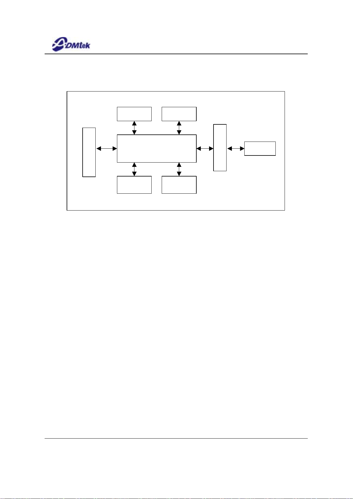
2. SYSTEM BLOCK DIAGRAM
AN983B
Transformer
RJ-45
Boot ROMEEPROM
LEDs
25MHz
Crystal
PCI Interface
Fig - 1 System diagram of the AN983B
ADMtek Inc.
www.admtek.com.tw
Rev. 1.8
10

AN983B PCI/miPCI Fast Ethernet Controller with integrated PHY
3. FEATURES
INDUSTRY STANDARD
IEEE802.3u 100BASE-TX and IEEE802.3 10BASE-T compliant
Support for IEEE802.3x flow control
IEEE802.3u Auto-Negotiation support for 10BASE-T and 100BASE-TX
PCI Specification 2.2 compliant
ACPI and PCI power management Ver.1.1 compliant
Support PC99 wake on LAN
FIFO
Provides two independent long FIFOs with 2k bytes each for transmission and receiving
Pre-fetch up to two transmit packets to minimize inter frame gap (IFG) to 0.96us
Retransmits collided packet without reload from host memory within 64 bytes.
Automatically retransmits FIFO under-run packet with maximum drain threshold until 3
times retry failure and that will not influence the registers and transmit threshold of next
packet
PCI I/F
Provides 32-bit PCI bus master data transfer
Supports PCI clock with frequency from 0Hz to 33MHz
Supports network operation with PCI system clock from 20MHz to 33MHz
Provides performance meter, PCI bus master latency timer, for tuning the threshold to
enhance the performance
Provides burst transmit packet interrupt and transmit/receive early interrupt to reduce
host CPU utilization
Supports memory-read, memory-read-line, memory-read-multiple, memory-write,
memory-write-and-invalidate command while being bus master
Supports big or little endian byte ordering
EEPROM/BOOT ROM I/F
Provides write-able Flash ROM and EPROM as boot ROM with size up to 128kB
Provides PCI to access boot ROM by byte, word, or double word
Re-writes Flash boot ROM through I/O port by programming register
ADMtek Inc.
www.admtek.com.tw
Rev. 1.8
11

AN983B PCI/miPCI Fast Ethernet Controller with integrated PHY
Provides serial interface for read/write 93C46/66 EEPROM
Automatically loads device ID, vendor ID, subsystem ID, subsystem vendor ID,
Maximum-Latency, and Minimum-Grand from the 64 byte contents of 93C46/66 after
PCI reset de-asserted in PCI environment.
MAC/PHYSICAL
Integrates the whole Physical layer functions of 100BASE-TX and 10BASE-T
Provides Full -duplex operation on both 100Mbps and 10Mbps modes
Provides Auto-negotiation (NWAY) function of full/half duplex operation for both 10 and
100 Mbps
Provides transmit wave-shaper, receive filters, and adaptive equalizer
Provides MLT-3 transceiver with DC restoration for Base-line wander compensation
Provides MAC and Transceiver (TXCVR) loop-back modes for diagnostic
Builds in Stream Cipher Scrambler/ De-scrambler and 4B/5B encoder/decoder
Supports external transmit transformer with turn ratio 1:1
Supports external receive transformer with turn ratio 1:1
LED DISPLAY
3 LEDs displays scheme provided:
100Mbps(on) or Speed 10(off)
Link (keeps on when link ok) or Activity (will be blinking with 10Hz when
receiving or transmitting but not collision)
FD (keeps on when in Full duplex mode) or Collision (will be blinking with 20Hz
when colliding)
4 LEDs displayed scheme provided:
100Mbps and Link (keep on when link and 100Mpbs)
10Mbps and Link (keep on when link and 10Mpbs)
Activity (will be blinking with 10Hz when receiving or transmitting but not
collision)
FD (keeps on when in Full duplex mode) or Collision (will be blinking with 20Hz
when colliding)
MISCELLANEOUS
Provides 128-pin QFP/LQFP packages for PCI/mini-PCI interfaces
3.3V power supply with 5V/3.3V I/O tolerance
ADMtek Inc.
www.admtek.com.tw
Rev. 1.8
12

AN983B PCI/miPCI Fast Ethernet Controller with integrated PHY
4. BLOCK DIAGRAM
CR /CS R /XR
Registers
PCI I/F
Control
Boot ROM
I/F
EEPROM
I/F
DMA
Control
Transit
FIFO
Receive
FIFO
FIFO
Control
Power M anagement
Control
LEDs
Display
Transmit
MAC
Receive
MAC
Loop-back
Control
Clock
Generator
100BA SE-TX
10BAS E-T
Physical
Medium
I/F
Fig - 2 Block diagram of the AN983B
ADMtek Inc.
www.admtek.com.tw
Rev. 1.8
13

AN983B PCI/miPCI Fast Ethernet Controller with integrated PHY
5. PIN ASSIGNMENT DIAGRAM
bra 12
bra 11/Mdc
bra 10/Mtxen
BrCS#
EECS
BrD7/ECK
BrD6/EDI
BrD5/EDO
BrD4/Mrxdv
BrD3/MrxD3
BrD2/MrxD2
BrD1/MrxD1
BrD0/MrxD0
BrWE#/Rxclk
BrOE#/Txclk
bra 9/MtxD3
bra 8/MtxD2
Vdd-3
bra 7/MtxD1
bra 6/MtxD0
bra 5/Mtxerr
Vss-3
bra 4
bra 16/LED-FD/C
o
LED-100Lnk
LED-10Lnk
128
127
126
125
124
123
122
121
120
119
118
117
116
115
114
113
112
111
110
109
108
107
106
105
104
103
bra 13 1 102 LED-Act
bra 14 2 101 bra 3/Mdio
bra 15 3 100 bra 2/Mcrs
VAAR 4 99 bra 1/Mcol
TST3 5 98 bra 0/Mrxerr
RXIN 6 97 PMEP
RXIP 7 96 Vcc_detect
GNDR 8 95 Vaux
TST0 9 94 AD0
TST1 10 93 AD1
TST2 11 92 clk-run
NC
12 91
Vss-pci
NC
13 90
AD2
GNDREEF
14 89
AD3
RIBB
15 88
AD4
VAAREF
16 87
Vdd-pci
XTLN 17 86 AD5
XTLP 18 85 AD6
GNDT 19 84 AD7
TXOP 20 83 CBEB0
TXON 21 82 Vss-pci
VAAT 22 81 AD 8
Vdd-IR 23 80 Vss-IR
INTA# 24 79 AD9
RST# 25 78 AD10
Vss-IR 26 77 Vdd-pci
pci_clk 27 76 AD11
Vdd-pci 28 75 AD12
gnt# 29 74 Vdd-IR
req# 30 73 AD13
pme# 31 72 AD14
Vss-pci 32 71 Vss-pci
AD31 33 70 AD15
AD30 34 69 CBEB1
AD29
35 68
PAR
AD28
36 67
Vdd-pci
Vdd-pci
37 66
SERR#
AD27
38 65
PERR#
39404142434445464748495051525354555657585960616263
64
AD26
AD25
AD24
Vss-pci
CBEB3
IDSEL
Vss-IR
AD23
AD22
Vdd-pci
AD21
AD20
AD19
Vss-pci
AD18
AD17
Vdd-IR
AD16
CBEB2
Vdd-pci
FRAME#
IRDY#
TRDY#
Vss-pci
DSEL#
STOP#
AN983B/AN983BL
Fig - 3 Pin assignment
ADMtek Inc.
www.admtek.com.tw
Rev. 1.8
14

AN983B PCI/miPCI Fast Ethernet Controller with integrated PHY
6. PIN DESCRIPTION
Pin # Name Type Description
PCI INTERFACE
24 INTA# O/D
PCI interrupt request. AN983B asserts this signal when one of the interrupt
events occurs.
25 RST# I
PCI signal to initialize the AN983B. The active reset signal should be
sustained at least 100µs to guarantee that the AN983B has completed the
initializing activity. During the reset period, all the output pins of AN983B
will be set to tri-state and all the O/D pins are floated.
27 PCI-CLK I
This PCI clock inputs to AN983B for PCI relative circuits as the synchronized
timing base with PCI bus. The Bus signals are recognized on rising edge of
PCI-CLK. In order to let network operating properly, the frequency range of
PCI-CLK is limited between 20MHz and 33MHz when network operating.
29 GNT# I
PCI Bus Granted. This signal indicates that the PCI bus request of AN983B
has been accepted.
30 REQ# O PCI Bus Request. Bus master device want to get bus access right
31 PME# I/O The Power Management Event signal is an open drain, active low signal.
When WOL-bit 18 of CSR 18 be set into “1”, means that the AN983B is set
into Wake On LAN mode. In this mode, when the AN983B receives a Magic
Packet frame from network then the AN983B will active this signal too.
In the Wake On LAN mode, when LWS-bit (bit 17) of CSR18 is set into “1”
means the LAN-WAKE signal is HP-style signal, otherwise it is IBM-style
signal.
33,34
35,36
38,39
40,41
46,47
49,50
51,53
54,56
70,72
73,75
76,78
79,81
84,85
86,88
89,90
93,94
AD-31, 30
AD-29, 28
AD-27, 26
AD-25, 24
AD-23, 22
AD-21, 20
AD-19, 18
AD-17, 16
AD-15, 14
AD-13, 12
AD-11, 10
AD-9, 8
AD-7, 6
AD-5, 4
AD-3, 2
AD-1, 0
I/O Multiplexed address data pin of PCI Bus
ADMtek Inc.
www.admtek.com.tw
Rev. 1.8
15

AN983B PCI/miPCI Fast Ethernet Controller with integrated PHY
43
57
69
83
C-BEB3
C-BEB2
C-BEB1
C-BEB0
I/O Bus command and byte enable
44 IDSEL I Initialization Device Select. This signal is asserted when host issues the
configuration cycles to the AN983B.
59 FRAME# I/O Begin and duration of bus access, driven by master device
60 IRDY# I/O Master device is ready to data transaction
61 TRDY# I/O Slave device is ready to data transaction
63 DEVSEL# I/O Device select, target is driving to indicate the address is decoded
64 STOP# I/O Target device request the master device to stop the current transaction
65 PERR# I/O Data parity error is detected, driven by the agent receiving data
66 SERR# O/D Address parity error
68 PAR I/O Parity, even parity (AD [31:0] + C/BE [3:0]), master drives par for address
and write data phase, target drives par for read data phase
92 Clk-run I/O
O/D
Clock Run for PCI system. In the normal operation situation, Host should
assert this signal to indicate AN983B about the normal situation. On the
other hand, when Host will deassert this signal when the clock is going down
to a non-operating frequency. When AN983B recognizes the deasserted
status of clk-run, then it will assert clk-run to request host to maintain the
normal clock operation. When clk-run function is disabled then the AN983B
will set clk-run in tri-state.
BOOTROM/EEPROM INTERFACE
98~101,
106,108
~110,
112,
113,
126,
127,
128,
1~3, 105
BrA0 ~16 I/O ROM data bus
Provides up to 128kB EPROM or Flash-ROM application space.
116~
120,
121~
123,
BrD0~4
BrD5/EDO
BrD6/EDI
BrD7/ECK
IO
IO/O
IO/I
IO/I
BootROM data bus bit (0~7)
Inputs/Output data for AN983B; EDO: Data Output of serial EEPROM
Inputs/Output data for AN983B; EDI: Data Input of serial EEPROM
Inputs/Output data for AN983B; ECK: Clock input of serial EEPROM, the
AN983B outputs clock signal to EEPROM
124 EECS O Chip Select of serial EEPROM
125 BrCS# O BootROM Chip Select
114 BrOE# O BootROM Read Enable for flash ROM application
ADMtek Inc.
www.admtek.com.tw
Rev. 1.8
16

AN983B PCI/miPCI Fast Ethernet Controller with integrated PHY
115 BrWE# O BootROM Write Enable for flash ROM application.
MII INTERFACE (PROGRAM AN983B AS MAC-ONLY MODE, SET
FCH [2:0] = 100B)
127 Mdc O MII Management Data Clock
126 Mtxen O MII Transmit Enable
109,110
112,113
MtxD0~3 O MII Transmit Data
108 Mtxerr O MII Transmit Error
101 Mdio I/O MII Management Data I/O
120 Mrxdv I MII Receive Data Valid
100 Mcrs I MII Carrier Sense
116 ~
119
MrxD0~3 I MII Receive Data
99 Mcol I MII Collision
98 Mrxerr I MII Receive Error
115 Rxclk I MII Receive Clock
114 Txclk I MII Transmit Clock
PHYSICAL INTERFACE
18, 17 XTLP, XTLN I Crystal inputs. To be connected to a 25MHz crystal with 50ppm accuracy
6,7 RXIN, RXIP I The different ials receive inputs of 100BASE-TX or 10BASE-T, these pins
directly input from Magnetic.
20,21 TXOP, TXON O The differential Transmit outputs of 100BASE-TX or 10BASE-T, t hese pins
directly output to Magnetic.
15 RIBB I Reference Bias Resistor. To be tied to an external 10.0K (1%) resistor which
should be connected to the analog ground at the other end.
9,10,11,
5
TST0, TST1
TST2, TST3
I Test pin
12,13 NC O
LED DISPLAY & MISCELLANEOUS
102 Led-Act
(Led-lnk/act)
O 4Leds mode: LED display for A c tivity status. This pin will be driven on with
10 Hz blinking frequency when either effective receiving or transmitting is
detected.
(3Led mode): LED display for link and activity status. This pin will be
driven on continually when a good Link test is detected. This pin will be
driven on with 10 Hz blinking frequency when either effective receiving or
transmitting is detected.
103 Led-10Lnk
(Led-fd/col)
O 4Leds mode: LED display for 10M b/s speed. This pin will be driven on
continually when the 10M b/s network operating speed is detected.
(3Leds mode): LED display for Full Duplex or Collision status. This pin will be
driven on continuall
y
when a full duplex configuration is detected. This pin
ADMtek Inc.
www.admtek.com.tw
Rev. 1.8
17

AN983B PCI/miPCI Fast Ethernet Controller with integrated PHY
will be driven on with 20 Hz blinking frequency when a collision status is
detected in the half duplex configuration.
104 Led-100Lnk
(Led-speed)
O 4Leds mode: LED display for 100Mb/s speed. This pin will be driven on
continually when the 100Mb/s network operating speed is detected.
(3Leds mode): LED display for 100M b/s or 10M b/s speed. This pin will be
driven on continually when the 100M b/s network operating speed is
detected.
105 Led-Fd /Col O 4Leds mode: LED display for Full Duplex or Collisio n status. This pin will be
driven on continually when a full duplex configuration is detected. This pin
will be driven on with 20 Hz blinking frequency when a collision status is
detected in the half duplex configuration.
(3Leds mode): None
95 Vaux I
When this pin is asserted, it indicates an auxiliary power source is supported
ACPI purpose, for detecting the auxiliary power source.
This pin should be or-wired connected to
1) 3.3V when 3.3Vaux support, or
2) 5V when 5Vaux support from 3-way switch.
96 Vcc-detect I When this pin is asserted, it indicates PCI power source is supported.
ACPI purpose, for detecting the main power is remained or not,
This pin should be connected to PCI bus power source +5V.
97 PMEP O This signal is used as the WOL pin. It provides a programmable positive or
negative pulse with approximately 50ms width.
DIGITAL POWER PINS
26,32,42,45,52,62,71,80,82,91,107, Vss-pci, Vss-IR, Vss-3
23,28,37,48,55,58,67,74,77,87,111 Vdd-pci Vdd-IR, Vdd-3
Connect to 3.3V
ANALOG POWER PINS
4,16,22 VAAR, VAAREF, VAAT
3.3V
8,14,19 GNDR, GNDREF, GNDT
ADMtek Inc.
www.admtek.com.tw
Rev. 1.8
18

AN983B PCI/miPCI Fast Ethernet Controller with integrated PHY
7. REGISTERS AND DESCRIPTORS DESCRIPTION
There are three kinds of registers designed for AN983B. They are AN983B configuration
registers, PCI control/status registers, and Transceiver control/status registers.
The AN983B configuration registers are used to initialize and configure the AN983B for
identifying and querying the AN983B.
The PCI control/status registers are used to communicate between host and AN983B. Host can
initialize, control, and read the status of the AN983B through the mapped I/O or memory address
space.
Regarding the registers of transceiver portion of AN983B, it includes 7 basic registers which are
defined according to the clause 22 “Reconciliation Sub-layer and Media Independent Interface”
and clause 28 “Physical Layer link signaling for 10 Mb/s and 100 Mb/s Auto-Negotiation on
twisted pair” of IEEE802.3u standard. The AN983B also provides receive and transmit
descriptors for packet buffering and management. These descriptors are described in the
following section
ADMtek Inc.
www.admtek.com.tw
Rev. 1.8
19

AN983B PCI/miPCI Fast Ethernet Controller with integrated PHY
7.1 AN983B CONFIGURATION REGISTERS
With the configuration registers software driver can initialize and configure AN983B. All of the
contents of configuration registers are set to default value when there is any hardware reset occurs.
On the other hand, there is no effect to their value when the software reset occurs. To access these
configuration registers AN983B provides byte, word, and double word data access length.
7.1.1. AN983B CONFIGURATION REGISTERS LIST
Offset Index Name Descriptions
00h
CR0 LID Loaded device ID and vendor ID
04h
CR1 CSC Configuration Status and Command
08h
CR2 CC Class Code and revision number
0ch
CR3 LT Latency Timer
10h
CR4 IOBA IO Base Address
14h
CR5 MBA Memory Base Address
28h
CR10 CIS Card Information Structure (for Card bus)
2ch
CR11 SID Subsystem ID and vendor ID
30h
CR12 BRBA Boot ROM Base Address (ROM size = 256KB)
34h
CR13 CP Capability Pointer
3ch
CR15 CINT Configuration Interrupt
40h
CR16 DS Driver space for special purpose
80h
CR32 SIG Signature of AN983B
c0h
CR48 PMR0 Power Management Register 0
c4h
CR49 PMR1 Power Management Register 1
ADMtek Inc.
www.admtek.com.tw
Rev. 1.8
20

AN983B PCI/miPCI Fast Ethernet Controller with integrated PHY
7.1.2. AN983B CONFIGURATION REGISTERS TABLE
Offset b31 ----------- b16 b15 ---------- b0
00h
Device ID* Vendor ID*
04h
Status Command
08h
Base Class
Code
Subclass ------ Revision # Step #
0ch
------ ------ Latency timer Cache line size
10h
Base I/O address
14h
Base memory address
18h~
24h
Reserved
28h
ROM-im* Address space offset* Add-indi*
2ch
Subsystem ID* Subsystem vendor ID*
30h
Boot ROM base address
34h
Reserved Cap_Ptr
38h
Reserved
3ch
Max_Lat* Min_Gnt* Interrupt pin Interrupt line
40h
Reserved Driver Space Reserved
80h
Signature of AN983B
c0h
PMC Next_Item_Ptr Cap_ID
c4h
Reserved PMCSR
Note:
* Automatically recalled from EEPROM when PCI reset is deserted
CIS (28h) is a read-only register
DS (40h), bit15-8, is read/write able register
SIG (80h) is hard wired register, read only.
ADMtek Inc.
www.admtek.com.tw
Rev. 1.8
21

AN983B PCI/miPCI Fast Ethernet Controller with integrated PHY
7.1.3 AN983B CONFIGURATION REGISTERS DESCRIPTIONS
CR0 (offset = 00h), LID - Loaded Identification number of Device and Vendor
Bit # Name Descriptions Default Val RW Type
31~16
LDID Loaded Device ID, the device ID number loaded from serial
EEPROM.
From
EEPROM
R/O
15~0
LVID Loaded Vendor ID, the vendor ID number loaded from serial
EEPROM.
From
EEPROM
R/O
From EEPROM: Loaded from EEPROM
CR1 (offset = 04h), CSC - Configuration command and status
Bit # Name Descriptions Default Val RW Type
31
SPE Status of Parity Error.
1: means that AN983B detected a parity error. This bit will
be set in this condition, even if the parity error response (bit
6 of CR1) is disabled.
0 R/W
30
SES Status of System Error.
1: means that AN983B asserted the system error pin.
0 R/W
29
SMA Status of Master Abort.
1: means that AN983B received a master abort and
terminated a master transaction.
0 R/W
28
STA Status of Target Abort.
1: means that AN983B received a target abort and
terminated a master transaction.
0 R/W
27
--- Reserved.
26, 25
SDST Status of Device Select Timing. The timing of the assertion of
device select.
01: means a medium assertion of DEVSEL#
01 R/O
24
SDPR Status of Data Parity Report.
1: when three conditions are met:
AN983B asserted parity error - PERR# or it detected parity
error asserted by other device.
AN983B is operating as a bus master.
AN983B’s parity error response bit (bit 6 of CR1) is enabled.
0 R/W
23
SFBB Status of Fast Back-to-Back
Always 1, since AN983B has the ability to accept fast
back-to-back transactions.
1 R/O
22~21
--- Reserved.
20
NC New Capabilities. This bit indicates that whether the AN983B
provides a list of extended capabilities, such as PCI power
management.
Same as
bit 19 of
CSR18
RO
ADMtek Inc.
www.admtek.com.tw
Rev. 1.8
22

AN983B PCI/miPCI Fast Ethernet Controller with integrated PHY
1: the AN983B provides the PCI management function
0: the AN983B doesn’t provide New Capabilities.
19~ 9
--- Reserved.
8
CSE Command of System Error Response
1: enable system error response. AN983B will assert SERR#
When it find a parity error on the address phase.
0 R/W
7
--- Reserved.
6
CPE Command of Parity Error Response
0: disable parity error response. AN983B will ignore any
detected parity error and keep on its operating. Default
value is 0.
1: enable parity error response. AN983B will assert system
error (bit 13 of CSR5) when a parity error is detected.
0 R/W
5~ 3
--- Reserved.
2
CMO Command of Master Operation Ability
0: disable the bus master ability.
1: enable the PCI bus master ability. Default value is 1 for
normal operation.
0 R/W
1
CMSA Command of Memory Space Access
0: disable the memory space access ability.
1: enable the memory space access ability.
0 R/W
0
CIOSA Command of I/O Space Access
1: enable the I/O space access ability.
0: disable the I/O space access ability.
0 R/W
R/W: Read and Write able. RO: Read able only.
CR2 (offset = 08h), CC - Class Code and Revision Number
Bit # Name Descriptions Default Val RW Type
31~24
BCC Base Class Code. It means AN983B is network controller. 02h RO
23~16
SC Subclass Code. It means AN983B is a Fast Ethernet
Controller.
00h RO
15~ 8
--- Reserved.
7 ~ 4
RN Revision Number identifies the revision number of AN983B. 01h RO
3 ~ 0
SN Step Number, identifies the AN983B steps within the current
revision.
01h RO
RO: Read Only.
CR3 (offset = 0ch), LT - Latency Timer
Bit # Name Descriptions Default Val RW Type
31~16
--- Reserved.
15~ 8
LT Latency Timer. This value specifies the latency timer of the
AN983B in units of PCI bus clock. Once the AN983B asserts
FRAME#, the latenc
y
timer starts to count. If the latency
0 R/W
ADMtek Inc.
www.admtek.com.tw
Rev. 1.8
23

AN983B PCI/miPCI Fast Ethernet Controller with integrated PHY
timer expires and the AN983B still asserted FRAME#, then the
AN983B will terminate the data transaction as soon as its
GNT# is removed.
7 ~ 0
CLS Cache Line Size. This value specifies the system cache line
size in units of 32-bit double words (DW). The AN983B
supports 8, 16, and 32 DW of cache line size. This value is
used by the AN983B driver to program the cache alignment
bits (bit 14 and 15 of CSR0). The cache alignment bits are
used for cache oriented PCI commands; say
memory-read-line, memory-read-multiple, and
memory-write-and-invalidate.
0 R/W
CR4 (offset = 10h), IOBA - I/O Base Address
Bit # Name Descriptions Default Val RW Type
31~ 8
IOBA I/O Base Address. This value indicate the base address of PCI
control and status register (CSR0~28)
0 R/W
7 ~ 1
--- Reserved.
0
IOSI I/O Space Indicator.
1: means that the configuration registers map into the I/O
space.
1 RO
CR5 (offset = 14h), MBA - Memory Base Address
Bit # Name Descriptions Default Val RW Type
31~ 10
MBA Memory Base Address. This value indicate the base address
of PCI control and status register (CSR0~28)
0 R/W
9 ~ 1
--- Reserved.
0
IOSI Memory Space Indicator.
1: means that the configuration registers map into the I/O
space.
0 RO
CR11 (offset = 2ch), SID - Subsystem ID.
Bit # Name Descriptions Default Val RW Type
31~16
SID Subsystem ID. This value is loaded from EEPROM after power
on or hardware reset.
From
EEPROM
RO
15~ 0
SVID Subsystem Vendor ID. This value is loaded from EEPROM after
power on or hardware reset.
From
EEPROM
RO
CR12 (offset = 30h), BRBA - Boot ROM Base Address.
Bit # Name Descriptions Default Val RW Type
31~17
BRBA Boot ROM Base Address. This value indicates the address
mapping of boot ROM field. Besides, it also defines the boot
ROM size. The value of bit 17~10 is set to 0 for AN983B
supports up to 256KB of boot ROM.
X: b31~18
0: b17~10
R/W
RO
16 ~ 1
--- Reserved 0 RO R/W
ADMtek Inc.
www.admtek.com.tw
Rev. 1.8
24

AN983B PCI/miPCI Fast Ethernet Controller with integrated PHY
R/W
0
BRE Boot ROM Enable. The AN983B really enables its boot ROM
access only if both the memory space access bit (bit 1 of
CR1) and this bit are set to 1.
1: enable Boot ROM. (Combines with bit 1 of CR1)
0 R/W
This register should be initialized before accessing the boot ROM space. (Write 32’hffffffff return 32’h
fffe0001)
CR13 (offset = 34h), CP - Capabilities Pointer.
Bit # Name Descriptions Default Val RW Type
31~8
--- Reserved
7~0
CP Capabilities Pointer. C0h RO
CR15 (offset = 3ch), CI - Configuration Interrupt
Bit # Name Descriptions Default Val RW Type
31~24
ML Max_Lat register. This value indicates “how often” the
AN983B needs to access to the PCI bus in the units of 250ns.
This value is loaded from serial EEPROM after power on or
hardware reset.
From
EEPROM
RO
23~16
MG Min_Gnt register. This value indicates how long the AN983B
needs to retain the PCI bus ownership whenever it initiates a
transaction, in the units of 250ns. This value is loaded from
serial EEPROM after power on or hardware reset.
From
EEPROM
RO
15~ 8
IP Interrupt Pin. This value indicates which of the four interrupt
request pins that AN983B is connected.
Always 01h: means the AN983B connects to INTA#
01h RO
7 ~ 0
IL Interrupt Line. This value indicates which of the system
interrupt request lines the INTA# of AN983B is routed to. The
BIOS will fill this field when it initializes and configures the
system. The AN983B driver can use this value to determine
priority and vector information.
X R/W
CR16 (offset = 40h), DS - Driver Space for special purpose.
Bit # Name Descriptions Default Val RW Type
31~16
--- Reserved
15~8
DS Driver Space for special purpose. Since this area won’t be
cleared in the software reset. The AN983B driver can use this
R/W area for special purpose.
X R/W
7 ~ 0
--- Reserved
(offset = 80h), SIG - Signature of AN983B
Bit # Name Descriptions Default Val RW Type
31~16
DID Device ID, the device ID number of AN983B. 0981h RO
15~0
VID Vendor ID, the vendor ID number of ADM Technology Corp. 1317h RO
ADMtek Inc.
www.admtek.com.tw
Rev. 1.8
25

AN983B PCI/miPCI Fast Ethernet Controller with integrated PHY
CR48 (offset = c0h), PMR0, Power Management Register0.
Bit # Name Descriptions Default Val RW Type
31~27
PMES PME_Support.
The AN983B will assert PME# signal while in the D0, D1, D2,
D3 power state. The AN983B supports Wake-up from the
above states.
11111b RO
26
D2S D2_Support. The AN983B supports D2 Power Management
State.
1 RO
25
D1S D1_Support. The AN983B supports D1 Power Management
State.
1 RO
24~22
AUXC Aux Current. These three bits report the maximum 3.3 Vaux
current requirements for AN983B. If bit 31 of PMR0 is ‘1’, the
default value is 0101b, means AN983B need 100 mA to
support remote wake-up in D3cold power state.
010b RO
21
DSI The Device Specific Initialization bit indicates whether
special initialization of this function is required before the
generic class device driver is able to use it.
0: indicates that the function does not require a device
specific initialization sequence following transition to the D0
un-initialized state.
0 RO
20
--- Reserved. 0 RO
19
PMEC PME Clock. When “1” indicates that the AN983B relies on the
presence of the PCI clock for PME# operation. While “0”
indicates the no PCI clock is required for the AN983B to
generate PME#.
0 RO
18~16
VER Version. The value of 010b indicates that the AN983B
complies with Revision 1.1
of the PCI Power Management
Interface Specification.
010b
RO
15~8
NIP Next Item Pointer. This value is always 0h, indicates that
there is no additional items in the Capabilities List.
00h
RO
7~0
CAPID Capability Identifier. This value is always 01h, indicates the
link list item as being PCI Power Management Registers.
01h RO
CR49 (offset = c4h), PMR1, Power Management Register 1.
Bit # Name Descriptions Default Val RW Type
31~16
--- Reserved
15
PMES PME_Status, This bit is set when the AN983B would normally
assert the PME# signal for wake-up event, this bit is
independent of the state of the PME-En bit.
Writing a “1” to this bit will clear it and cause the AN983B to
stop asserting a PME# (if enabled). Writing a “0” has no
effect.
0 R/W*
14,13
DSCAL Data_Scale, indicates the scaling factor to be used when 00b RO
ADMtek Inc.
www.admtek.com.tw
Rev. 1.8
26

AN983B PCI/miPCI Fast Ethernet Controller with integrated PHY
interpreting the value of the Data register. This field is
required for any function that implements the Data register.
Otherwise, it’s optional.
The AN983B doesn’t support Data register and Data_Scale.
12~9
DSEL Data_Select, This four-bit field is used to select which data
is to be reported through the Data register and Data_Scale
field. This field is required for any function that implements
the Data register.
The AN983B doesn’t support Data_select.
0000b R/W
8
PME_En PME_En, “1” enables the AN983B to assert PME#. When “0”
disables the PME# assertion.
Magic packet default enable:
When Csr18<18> and csr18<19> are set to 1, than the magic
packet wake up event will be default enabled (csr13<9> be
set) it doesn’t matter the PME_En is set or not.
0
R/W
7~2
--- Reserved. 000000b RO
1,0
PWRS PowerState, This two-bit field is used both to determine the
current power state of the AN983B and to set the AN983B
into a new power state. The definition of this field is given
below.
00b - D0
01b - D1
10b - D2
11b - D3hot
This field is auto cleared to D0 when power resumed.
00b R/W
R/W*: Read and Write clear
ADMtek Inc.
www.admtek.com.tw
Rev. 1.8
27

AN983B PCI/miPCI Fast Ethernet Controller with integrated PHY
7.2. PCI CONTROL/STATUS REGISTERS
7.2.1. PCI CONTROL/STATUS REGISTERS LIST
Offset from
base address of
CSR
Index Name Descriptions
00h
CSR0 PAR PCI access register
08h
CSR1 TDR Transmit demand register
10h
CSR2 RDR Receive demand register
18h
CSR3 RDB Receive descriptor base address
20h
CSR4 TDB Transmit descriptor base address
28h
CSR5 SR Status register
30h
CSR6 NAR Network access register
38h
CSR7 IER Interrupt enable register
40h
CSR8 LPC Lost packet counter
48h
CSR9 SPR Serial port register
50h
CSR10 --- Reserved
58h
CSR11 TMR Timer
60h
CSR12 --- Reserved
68h
CSR13 --- Reserved
70h
CSR14 --- Reserved
78h
CSR15 WTMR Watchdog timer
80h
CSR16 ACSR5 Status register 2
84h
CSR17 ACSR7 Interrupt enable register 2
88h
CSR18 CR Command register
8ch
CSR19 PCIC PCI bus performance counter
90h
CSR20 PMCSR Power Management Command and Status
94h
CSR21 WTDP Current transmit descriptor point
98h
CSR22 WRDP Current receive descriptor point
9ch
CSR23 TXBR Transmit burst counter/time-out register
a0h
CSR24 FROM Flash (boot) ROM port
a4h
CSR25 PAR0 Physical address register 0
a8h
CSR26 PAR1 Physical address register 1
ach
CSR27 MAR0 Multicast address hash table register 0
b0h
CSR28 MAR1 Multicast address hash table register 1
fch
OPR Operation Mode register
ADMtek Inc.
www.admtek.com.tw
Rev. 1.8
28
 Loading...