

ADMTK ADM7008 Datasheet

ADM7008
Octal Ethernet 10/100M PHY
Datasheet
Version 1.0
ADMtek.com.tw
Information in this document is provided in connection with ADMtek products. ADMtek may make
changes to specifications and product descriptions at any time, without notice. Designers must not rely on
the absence or characteristics of any features or instructions marked “reserved” or “undefined”. ADMtek
reserves these for future definition and shall have no responsibility whatsoever for conflicts or
incompatibilities arising from future changes to them
The products may contain design defects or errors know as errata, which may cause the product to deviate
from published specifications. Current characterized errata are available on request. To obtain latest
documentation please contact you local ADMtek sales office or visit ADMtek’s website at
http://www.ADMtek.com.tw
*Third-party brands and names are the property of their respective owners.
Copyright 2003 by ADMtek Incorporated All Rights Reserved

ADMtek Inc. V1.0
About this Manual
Intended Audience
Structure
This Data sheet contains 6 chapters
Chapter 1 Product Overview
Chapter 2 Interface Description
Chapter 3 Function Description
Chapter 4. Register Description
Chapter 5. Electrical Specification
Chapter 6. Packaging
Revision History
Date Version Change
23 January 2003
1.0 First release of ADM7008
Customer Support
ADMtek Incorporated,
2F, No.2, Li-Hsin Rd.,
Science-based Industrial Park,
Hsinchu, 300, Taiwan, R.O.C.
Sales Information
Tel + 886-3-5788879
Fax + 886-3-5788871
ADM7008

ADMtek Inc. V1.0
Table of Contents
Chapter 1 Product Overview ........................................................................................ 1-1
1.1 Overview.......................................................................................................... 1-1
1.2 Features............................................................................................................1-2
1.3 Block Diagram.................................................................................................1-3
1.4 Abbreviations...................................................................................................1-3
1.5 Conventions ..................................................................................................... 1-5
1.5.1 Data Lengths............................................................................................ 1-5
1.5.2 Register Type Descriptions...................................................................... 1-5
1.5.3 Pin Type Descriptions.............................................................................. 1-5
Chapter 2 Interface Description................................................................................... 2-1
2.1 Pin Diagram ..................................................................................................... 2-1
2.2 Pin Description................................................................................................. 2-2
2.2.1 Twisted Pair Interface, 32 pins................................................................ 2-2
2.2.2 Ground and Power, 20 pins..................................................................... 2-2
2.2.3 Mode Setting ............................................................................................2-2
2.2.4 Clock Input Select .................................................................................... 2-2
2.2.5 Clock Input, 3 pins ................................................................................... 2-3
2.2.6 RMII/SMII Interface, 48 pins................................................................... 2-3
2.2.7 ATPG Signals, 2 pins ............................................................................. 2-16
2.2.8 Reset Pin ................................................................................................ 2-16
2.2.9 Control Signals, 3 pins........................................................................... 2-16
2.2.10 LED Interface, 2 pins............................................................................. 2-17
2.2.11 Regulator Control, 2 pins ......................................................................2-17
2.2.12 Digital Power/Ground, 13 pins.............................................................. 2-17
Chapter 3 Function Description ................................................................................... 3-1
3.1 10/100M PHY Block .......................................................................................3-2
3.1.1 100Base-X Module................................................................................... 3-2
3.1.2 100Base-TX Receiver............................................................................... 3-2
3.1.3 100Base-TX Transmitter.......................................................................... 3-7
3.1.4 100Base-FX Receiver............................................................................... 3-7
3.1.5 100Base-FX Transmitter.......................................................................... 3-8
3.1.6 10Base-T Module..................................................................................... 3-8
3.1.7 Operation Modes .....................................................................................3-8
3.1.8 Manchester Encoder/Decoder ................................................................. 3-8
3.1.9 Transmit Driver and Receiver .................................................................3-9
3.1.10 Smart Squelch ..........................................................................................3-9
3.1.11 Carrier Sense ........................................................................................... 3-9
3.1.12 Collision Detection ................................................................................ 3-10
3.1.13 Jabber Function..................................................................................... 3-10
3.1.14 Link Test Function ................................................................................. 3-10
3.1.15 Automatic Link Polarity Detection ........................................................ 3-11
3.1.16 Clock Synthesizer................................................................................... 3-11
3.1.17 Cable Broken Auto Detection ................................................................3-11
3.1.18 Auto Negotiation .................................................................................... 3-12
3.1.19 Auto Negotiation and Speed Configuration........................................... 3-13
ADM7008 i

ADMtek Inc. V1.0
3.2 MAC Interface ............................................................................................... 3-13
3.2.1 Reduced Media Independent Interface (RMII) ...................................... 3-14
3.2.2 Receive Path for 100M........................................................................... 3-14
3.2.3 Receive Path for 10M............................................................................. 3-16
3.2.4 Transmit Path for 100M ........................................................................ 3-16
3.2.5 Transmit Path for 10M .......................................................................... 3-16
3.2.6 Serial and Source Synchronous Media Independent Interface.............. 3-17
3.2.7 100M Receive Path ................................................................................ 3-18
3.2.8 10M Receive Path .................................................................................. 3-19
3.2.9 100M Transmit Path .............................................................................. 3-20
3.2.10 10M Transmit Path ................................................................................ 3-20
3.3 LED Display ..................................................................................................3-21
3.3.1 Single Color LED................................................................................... 3-21
3.3.2 Dual Color LED..................................................................................... 3-23
3.3.3 Serial Output LED Status ...................................................................... 3-23
3.3.4 RMII Mode (RSMODE1 = 1)................................................................. 3-24
3.3.5 SMII/SS_SMII Mode (RSMODE1 = 0).................................................. 3-24
3.4 Management Register Access........................................................................ 3-24
3.4.1 Preamble Suppression ...........................................................................3-25
3.4.2 Reset Operation .....................................................................................3-25
3.5 Power Management .......................................................................................3-26
3.5.1 Medium Detect Power Saving................................................................ 3-26
3.5.2 Transmit Power Saving.......................................................................... 3-27
3.6 Voltage Regulator .......................................................................................... 3-28
Chapter 4 Register Description .................................................................................... 4-1
4.1 Register Mapping.............................................................................................4-1
4.2 Register Bit Mapping....................................................................................... 4-2
4.2.1 Register #0h -- Control Register.............................................................. 4-2
4.2.2 Register #1h – Status Register ................................................................. 4-2
4.2.3 Register #2h – PHY ID Register (002E) .................................................. 4-2
4.2.4 Register #3h – PHY ID Register (CC11) ................................................. 4-2
4.2.5 Register #4h – Advertisement Register .................................................... 4-2
4.2.6 Register #5h – Link Partner Ability Register........................................... 4-2
4.2.7 Register #6h – Auto Negotiation Expansion Register.............................. 4-2
4.2.8 Register #7h – # Fh Reserved .................................................................. 4-2
4.2.9 Register #10h – PHY Configuration Register.......................................... 4-2
4.2.10 Register #11h – 10M Configuration Register.......................................... 4-3
4.2.11 Register #12h – 100M Configuration Register........................................ 4-3
4.2.12 Register #13h – LED Configuration Register.......................................... 4-3
4.2.13 Register #14h – Interrupt Enable Register .............................................. 4-3
4.2.14 Register #16h – PHY Generic Status Register......................................... 4-3
4.2.15 Register #17h – PHY Specific Status Register......................................... 4-3
4.2.16 Register #18h – Recommend Value Storage Register ............................. 4-3
4.2.17 Register #19h – Interrupt Status Register................................................ 4-3
4.2.18 Register #1dh – Receive Error Counter .................................................. 4-4
4.2.19 Register #1eh – Chip ID (8888
) ............................................................... 4-4
ADM7008 ii

ADMtek Inc. V1.0
4.2.20 Register #1fh –Total Interrupt Status (only For Port 0).......................... 4-4
4.3 Register Description......................................................................................... 4-4
4.3.1 Control (Register 0h) ............................................................................... 4-4
4.3.2 Status (Register 1h).................................................................................. 4-6
4.3.3 PHY Identifier Register (Register 2h)...................................................... 4-8
4.3.4 PHY Identifier Register (Register 3h)...................................................... 4-8
4.3.5 Advertisement (Register 4h)..................................................................... 4-9
4.3.6 Auto Negotiation Link Partner Ability (Register 5h)............................. 4-10
4.3.7 Auto Negotiation Expansion Register (Register 6h).............................. 4-11
4.3.8 Register Reserved (Register 7h-Fh).......................................................4-11
4.3.9 Generic PHY Configuration Register (Register 10h) ............................ 4-11
4.3.10 PHY 10M Module Configuration Register (Register 11h) ....................4-12
4.3.11 PHY 100M Module Control Register (Register 12h)............................. 4-13
4.3.12 LED Configuration Register (Register 13h).......................................... 4-13
4.3.13 Interrupt Enable Register (Register 14h) ..............................................4-15
4.3.14 PHY Generic Status Register (Register 16h)......................................... 4-16
4.3.15 PHY Specific Status Register (Register 17h) ......................................... 4-17
4.3.16 PHY Recommend Value Status Register (Register 18h)........................ 4-18
4.3.17 Interrupt Status Register (Register 19h)................................................ 4-18
4.3.18 Receive Error Counter Register (Register 1Dh).................................... 4-19
4.3.19 Chip ID Register (Register 1Fh)............................................................4-20
4.3.20 Per port Interrupt and Revision ID Register (Register 1Eh)................. 4-20
Chapter 5 Electrical Specification................................................................................ 5-1
5.1 DC Characterization......................................................................................... 5-1
5.1.1 Absolute Maximum Rating....................................................................... 5-1
5.1.2 Recommended Operating Conditions ...................................................... 5-1
5.1.3 DC Electrical Characteristics for 3.3V Operation.................................. 5-1
5.2 AC Characterization......................................................................................... 5-2
5.2.1 XI/OSCI (Crystal/Oscillator) Timing....................................................... 5-2
5.3 RMII Timing.................................................................................................... 5-3
5.3.1 REFCLK Input Timing (When REFCLK_SEL is set to 1) .......................5-3
5.3.2 REFCLK Output Timing (When REFCLK_SEL is set to 0)..................... 5-4
5.3.3 RMII Transmit Timing .............................................................................5-5
5.3.4 RMII Receive Timing ...............................................................................5-6
5.4 SMII Clock Timing..........................................................................................5-7
5.4.1 REFCLK Input Timing (When REFCLK_SEL is set to 1) -..................... 5-7
5.4.2 REFCLK Output Timing (When REFCLK_SEL is set to 1)..................... 5-8
5.4.3 SMII/SS_SMII Transmit Timing............................................................... 5-9
5.4.4 SMII/SS_SMII Receive Timing............................................................... 5-10
5.5 Serial Management Interface (MDC/MDIO) Timing.................................... 5-11
5.6 Power On Configuration Timing ................................................................... 5-12
Chapter 6 Packaging...................................................................................................... 6-1
ADM7008 iii

ADMtek Inc. V1.0
List of Figures
Figure 1-1 ADM7008 Block Diagram.......................................................................................1-3
Figure 2-1 ADM7008 Pin Assignment ......................................................................................2-1
Figure 3-1 ADM7008 Switch Application (10/100M TP Mode) ..................................................... 3-1
Figure 3-2 100Base-X Block Diagram and Data Path................................................................... 3-3
Figure 3-3 10Base-T Block Diagram and Data Path................................................................... 3-10
Figure 3-4 RMII Signal Diagram ...........................................................................................3-14
Figure 3-5 RMII Reception Without Error ...............................................................................3-15
Figure 3-6 RMII Reception with False Carrier (100M Only)........................................................ 3-15
Figure 3-7 RMII Reception with Symbol Error ......................................................................... 3-15
Figure 3-8 10M RMII Receive Diagram .................................................................................. 3-16
Figure 3-9 100M RMII Transmit Diagram ............................................................................... 3-16
Figure 3-10 10M RMII Transmit Diagram ............................................................................... 3-17
Figure 3-11 SMII Signal Diagram .......................................................................................... 3-18
Figure 3-12 SS_SMII Signal Diagram..................................................................................... 3-18
Figure 3-13 100M SMII Receive Timing Diagram .................................................................... 3-18
Figure 3-14 100M SS_SMII Receive Timing Diagram ...............................................................3-18
Figure 3-15 10M SMII Receive Timing Diagram ...................................................................... 3-19
Figure 3-16 10M SS_SMII Receive Timing Diagram................................................................. 3-19
Figure 3-17 100M SMII Transmit Timing Diagram ...................................................................3-20
Figure 3-18 100M SS_SMII Transmit Timing Diagram.............................................................. 3-20
Figure 3-19 10M SMII Transmit Timing Diagram..................................................................... 3-20
Figure 3-20 10M SS_SMII Transmit Timing Diagram ............................................................... 3-21
Figure 3-21 Stream LED under RMII Mode............................................................................. 3-24
Figure 3-22 Stream LED under SMII/SS_SMII Mode................................................................ 3-24
Figure 3-23 SMI Read Operation ...........................................................................................3-25
Figure 3-24 SMI Write Operation...........................................................................................3-25
Figure 3-25 Medium Detect Power Management Flow Chart.......................................................3-27
Figure 3-26 Low Power Link Pulse during TX for Power Management .........................................3-28
Figure 3-27 External PNP Power Transistor Diagram................................................................. 3-29
Figure 5-1 Crystal/Oscillator Timing ........................................................................................ 5-2
Figure 5-2 REFCLK Input Timing ...........................................................................................5-3
Figure 5-3 REFCLK Output Timing ......................................................................................... 5-4
Figure 5-4 RMII Transmit Timing............................................................................................ 5-5
Figure 5-5 RMII Receive Timing ............................................................................................. 5-6
Figure 5-6 REFCLK Input Timing ...........................................................................................5-7
Figure 5-7 SMII/SS_SMII REFCLK Output Timing.................................................................... 5-8
Figure 5-8 SMII/SS_SMII Transmit Timing............................................................................... 5-9
Figure 5-9 SMII/SS_SMII Receive Timing .............................................................................. 5-10
Figure 5-10 Serial Management Interface (MDC/MDIO) Timing ................................................. 5-11
Figure 5-11 Power On Configuration Timing ...........................................................................5-12
ADM7008 iv

ADMtek Inc. V1.0
List of Tables
Table 3-1 Look-up Table for translating 5B Symbols into 4B Nibbles. ............................................3-5
Table 3-2 Channel Configuration ........................................................................................... 3-17
Table 3-3 Receive Data Encoding for SMII/SS_SMII mode ........................................................ 3-19
Table 3-4 Speed LED Display ............................................................................................... 3-21
Table 3-5 Duplex LED Display ............................................................................................. 3-22
Table 3-6 Activity/Link LED Display ..................................................................................... 3-22
Table 3-7 Different Blinking Time for Different Speed .............................................................. 3-22
Table 3-8 Cable Distance LED Display ................................................................................... 3-22
Table 3-9 Speed LED Display ............................................................................................... 3-23
Table 3-10 Activity/Link LED Display ................................................................................... 3-23
Table 5-1 Electrical Absolute Maximum Rating.......................................................................... 5-1
Table 5-2 Recommended Operating Conditions .......................................................................... 5-1
Table 5-3 DC Electrical Characteristics for 3.3V Operation........................................................... 5-1
Table 5-4 Crystal/Oscillator Timing ......................................................................................... 5-2
Table 5-5 REFCLK Input Timing ............................................................................................ 5-3
Table 5-6 REFCLK Output Timing .......................................................................................... 5-4
Table 5-7 RMII Transmit Timing............................................................................................. 5-5
Table 5-8 RMII Receive Timing .............................................................................................. 5-6
Table 5-9 REFCLK Input Timing ............................................................................................ 5-7
Table 5-10 SMII/SS_SMII REFCLK Output Timing ...................................................................5-8
Table 5-11 SMII/SS_SMII Transmit Timing ..............................................................................5-9
Table 5-12 SMII/SS_SMII Receive Timing.............................................................................. 5-10
Table 5-13 Serial Management Interface (MDC/MDIO) Timing ..................................................5-11
Table 5-14 Power On Configuration Timing.............................................................................5-12
ADM7008 v

ADM7008 Product Review
Chapter 1 Product Overview
1.1 Overview
The ADM7008 is a single chip eight port 10/100M PHY, which is designed for today’s
low cost and low power dual speed application.
It supports eight auto sensing 10/100 Mbps ports with on-chip clock recovery and base
line wander correction including integrated MLT-3 functionality for 100 Mbps operation.
It also supports Manchester Code Converter with on chip clock recovery circuitry for 10
Mbps functionality, provides Reduced MII (RMII), Serial MII (SMII) and Source
Synchronous MII (SS_SMII) interface to facilitate high port count switch system
application and reduce the pin number simultaneously.
For today’s Information Application (IA), ADM7008 also supports “Auto Cross Over
Detection” function to eliminate the technical barrier between networking and the end
user. With the aid of this auto cross over detection function, Plug-n-Play features can be
easily applied to IA relative products.
To make the user interface as friendly as possible, ADM7008 provides cable length
information for CAT5 cable and also detects that the wire connection on the RJ-45 is
broken or not. This function is specifically helpful in system debugging, especially for
high port count approach system debugging.
The major design goal for ADM7008 is to reduce the power consumption and system
radiation for the whole system. With the aid of this low power consumption and low
radiation chip, fan and on-system power supply can be removed to save the total
manufacture cost and make SOHO application achievable.
ADMtek Inc. 1-1

ADM7008 Product Review
1.2 Features
• IEEE 802.3 compatible (2000 edition) 10BASE-T and 100BASE-T physical layer
interface and ANSI X3.263 TP-PMD compatible transceiver.
• Eight-port, single chip, integrated physical layer and transceivers for 10BASE-T and
100BASE-TX function.
• Reduced MII (RMII), Serial MII (SMII) and Source Synchronous MII (SS_SMII) for
high port count switch.
• Built-in 10Mbit transmit filter.
• 10 Mbit PLL, exceeding tolerances for both preamble and data jitter.
• 100Mbit PLL, combined with the digital adaptive equalizer and performance exceeds
140 meters for UTP 5.
• 125MHz Clock Generator and Timing Recovery.
• Integrated Base Line Wander Correction.
• Carrier Integrity Monitor function supported.
• Supports FEFI when Auto Negotiation is disabled.
• Supports Auto Cross Over Detection function for Plug-and-Play.
• IEEE 802.3u Clause 28 compliant auto negotiation for full 10 Mbps and 100 Mbps
control.
• Supports programmable LED for different Switch Application and Power On LED
Self Test.
• Supports Cable Length Indication both in MII Register and LED (Programmable).
• Supports Cable Broken Auto Detection function and indicate cable broken location.
• Supports PECL interface for fiber connection.
• Built-in 3.3V to 1.8V Regulator Control Signal.
• Built-in Clock Generator and Power On Reset Signal to save system cost.
• 128 PQFP with 1.8V/3.3V Power Supply.
• Support Power saving function.
• Support Parallel/Serial LED output.
ADMtek Inc. 1-2
ADM7008 Product Review
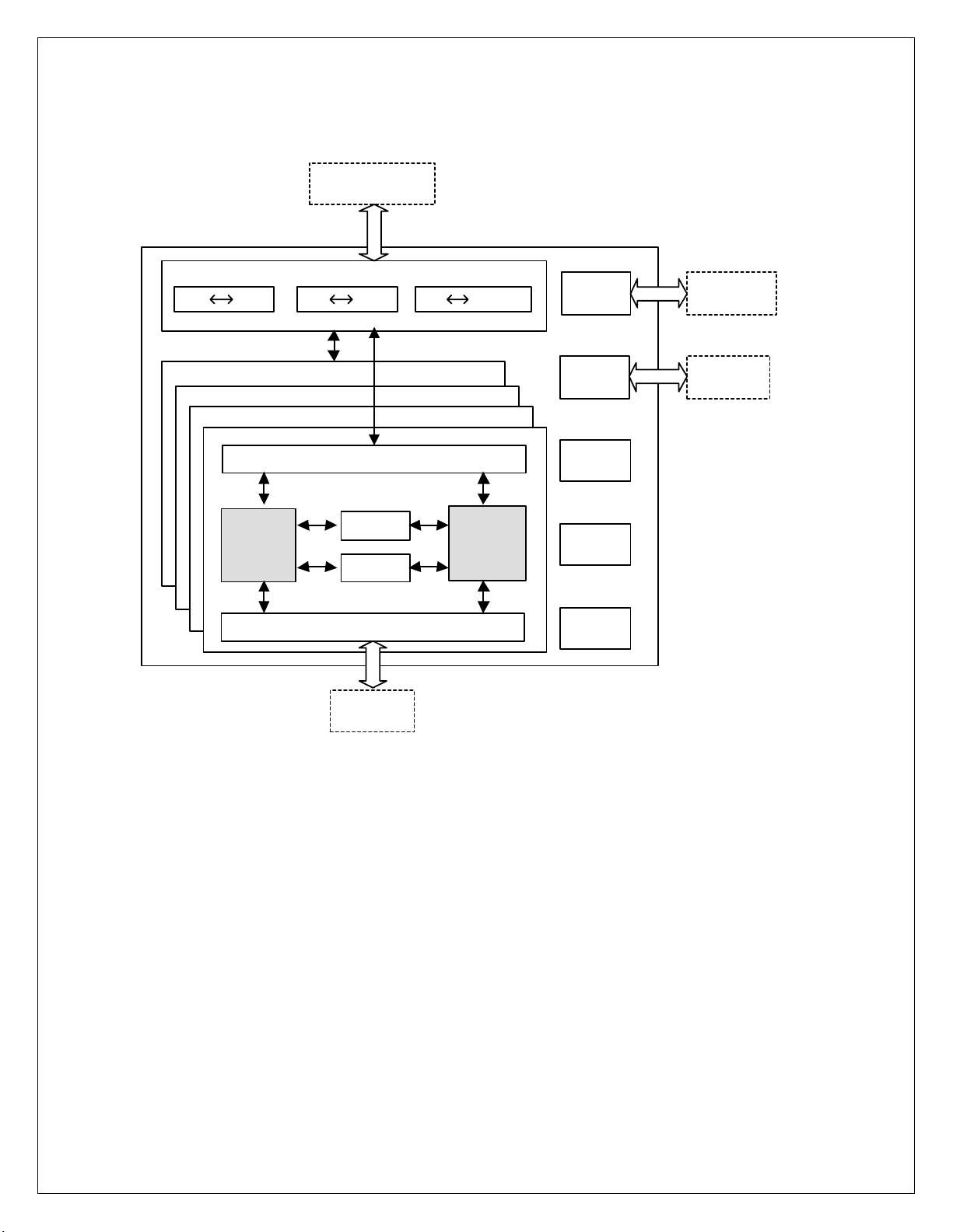
1.3 Block Diagram
RMII/SMII/
SS_SMII
PORT0
PORT1
...
PORT7
100M
Module
MAC Interface
MII RMII MII SS_S MIIMII SMII
MI I
Auto
Negotiation
Cable Broken
Detec tor
Driver
Twisted
Pair
Interface
10M
Module
LED
Display
SMI
Power
Management
CLOCK
GE NERAT OR
Voltage
Regulator
Serial /
Parallel
LED
MDC/MDIO
Figure 1-1 ADM7008 Block Diagram
1.4 Abbreviations
ANSI American National Standards Institute
BER Bit Error Rate
COL Collision
CRS Carrier Sense
CRSDV Carrier Sense and Data Valid
CTL Crystal
DSP Digital Signal Processor
DUPCOL Duplex and Collision
ESD End of Stream Delimiter
FEFI Far End Fault Indication
ADMtek Inc. 1-3

ADM7008 Product Review
FIFO First In First Out
FLP Fast Link Pulse
FX Fiber
IA Information Application
LFSR Linear Feedback Shifter Register
LLP Low-power Link Pulse
LNKACT Link and Activity
LVTTL TTL Level
MAC Media Access Controller
MD Medium Detect
MDC Management Data Clock
MDIO Management Data Input/Output
MII Media Independent Interface
NRZ None Return to Zero
NRZI None Return to Zero Inverter
OP Operation Code
PCS Physical Coding Sub-layer
PECL Pseudo Emitter Couple Logic
PHY Physical Layer
PHYADDR PHY Address
PMA Physical Medium Attachment
PMD Physical Medium Dependent
PNP A type of Transistor
PQFP Plastic Quad Flat Pack
REFCLK Reference Clock
RF Remote Fault
RMII Reduced Media Independent Interface
RSMODE RMII/SMII/SS_SMII Mode Select
RXC Receive Clock
RXD Receive Data
RXDV Receive Data Valid
RXER Receive Data Error
RXN Receive Negative (Analog receive differential signal)
RXP Receive Positive (Analog receive differential signal)
RX_SYNC Receive Synchronous
SDN Signal Detect Negative (Fiber signal detect)
SDP Signal Detect Positive (Fiber signal detect)
SELFX Select Fiber
SMI Serial Management Interface
SMII Serial Media Independent Interface
SOHO Small Office and Home Office
SQE Signal Quality Error
SSD Start of Stream Delimiter
SS_SMII Source Synchronous Media Independent Interface
SYNC Synchronous
TA Turn Around
ADMtek Inc. 1-4

ADM7008 Product Review
TDR Time Domain Reflectometry
TP Twisted Pair
TP-PMD Twisted Pair Physical Medium Dependent
TTL Transistor Transistor Logic
TXC Transmission Clock (MII)
TXCLK Transmission Clock (SMII/SS_SMII)
TXD Transmission Data
TXEN Transmission Enable
TXER Transmission Error
TXN Transmission Negative
TXP Transmission Positive
/J/K 5B signal to detect the start of a frame
/T/R 5B signal to detect the end of a frame
1.5 Conventions
1.5.1 Data Lengths
qword 64-bits
dword 32-bits
word 16-bits
byte 8 bits
nibble 4 bits
1.5.2 Register Type Descriptions
Register Type Description
RO Read Only
R/W Read and Write capable
SC Self-clearing
LL Latching low, unlatch on read
LH Latching high, unlatch on read
COR Clear On Read
1.5.3 Pin Type Descriptions
Pin Type Description
I: Input
O: Output
I/O: Bi-directional
OD: Open drain
SCHE: Schmitt Trigger
PU: Pull Up
PD: Pull Down
ADMtek Inc. 1-5

ADM7008 Interface Description
Chapter 2 Interface Description
2.1 Pin Diagram
118
117
116
119
120
123
122
128
127
126
125
RXN0
VCCAD
RXP0
GNDRT
1
RXN1
2
RXP1
3
GND RT
4
TXN1
5
TXP1
6
VCCA2
7
TXP2
8
TXN2
9
GND RT
10
RXP2
11
RXN2
12
VCCAD
13
RXN3
14
RXP3
15
GND RT
16
TXN3
17
TXP3
18
VCCA2
19
TXP4
20
TXN4
21
GND RT
22
RXP4
23
RXN4
24
VCCAD
25
RXN5
6
2
RXP5
27
GND RT
28
TXN5
29
TXP5
30
VCCA2
31
TXP6
32
TXN6
33
GND RT
34
RXP6
35
RXN6
36
VCCAD
37
RXN7
38
RXP7
TXN7
RSMODE1
VCCA2
TXP7
GNDRT
121
124
RTX
VCCPLL2
VCCA2
TXP0
TXN0
GNDRCV
Revision A1
PHYADDR1
REFCLK_SEL
VCC2I K
GNDIK
RST_N
115
VCCAD
XI
XO
CONTROL
QFP 128
(REC_10M_P7) RXD1_P7/SPEED_LED_P7
(EN_AUTOMDIX) RXD0_ P7/R XD_P 7
LED_ DATA
LED_ CLK
111
114
113
112
110
109
108
107
106
105
104
103
VCC3O
GNDO
RXD1_P0/SPDLED_P0 (REC_10M_P0)
RXD0 _P0 /RXD_P0 (TESTSEL0)
CRSDV_P0 (SELFX0)
TXD1_ P0 /LNKAC T_P0
TXD0_ P0/TXD_P0
TXEN_ P0 /NA
REFCLK
GNDIK
SCAN_ MODE
SCAN_ EN
102
MDC
101
MDIO
GND IK
GND O
VCC3O
GND IK
100
99
98
97
96
95
94
93
92
91
90
89
88
87
86
85
84
83
82
81
80
79
78
77
76
75
74
73
72
71
70
69
68
67
66
65
TXEN_ P1 /NA
TXD0 _P 1/TX D_P 1
TXD1_P1/LNKACT_P1
CRS DV_P1 /NA (SELFX1)
RXD0 _P1 /RXD_P1 (TESTSEL1)
RXD1_P1/SPDLED_P1 (REC_10M_P1)
RXD0 _P2 /RXD_P2 (PHYADDR0 )
ADM7008
(REC_10M_P6) RXD1_P6/SPEED_LED_P6
(FX_PAUS E) CRSDV_ P7
TXD1_P7/LNKACT_P7
TXD0_ P7/TXD_P7
TXEN_ P7 /NA
VCC3O
GNDO
RXD1_P2/SPDLED_P2 (REC_10M_P2)
CR SD V_ P3 /R X_ SYNC (TESTS EL2 )
RXD0 _P3 /RXD_P3 (ANENDIS)
RXD1_P3 /SPDLED_P3 (REC_10M_P3)
CRSDV_P4/RX_CLK (DLY2NS)
RXD0 _P4 /R XD_P4 (TPDUPLEX)
RXD1_P4 /SPDLED_P4 (REC_10M_P4)
(LEDMD0) RXD0 _ P6/R XD_P 6
(RSMODE0) CRSDV_P6/NA
TXD1_P6/LNKACT_P6
CRSDV_P5 /NA (TP_PAUSE)
RXD0_P5/RXD_P5 (PWSAVE_DIS)
RXD1_P5 /SPDLED_P5 (REC_10M_P5)
TXD0_ P6/TXD_P6
TXEN_ P6 /NA
TXEN_ P2 /NA
TXD0 _P 2/TX D_P 2
TXD1_P2/LNKACT_P2
CRS DV_P2 (FXDUPLEX)
VCC2I K
TXEN_P3/TX_SYNC
TXD0 _P 3/TX D_P 3
TXD1_P3/LNKACT_P3
TXEN_ P4 /TX_ CLK
TXD0 _P 4/TX D_P 4
TXD1_P4/LNKACT_P4
VCC2I K
TXEN_ P5 /NA
TXD0 _P 5/TX D_P 5
TXD1_P5/LNKACT_P5
46474849505152535455565758596061626364
45
44
43
424140
39
Figure 2-1 ADM7008 Pin Assignment
ADMtek Inc. 2-1

ADM7008 Interface Description
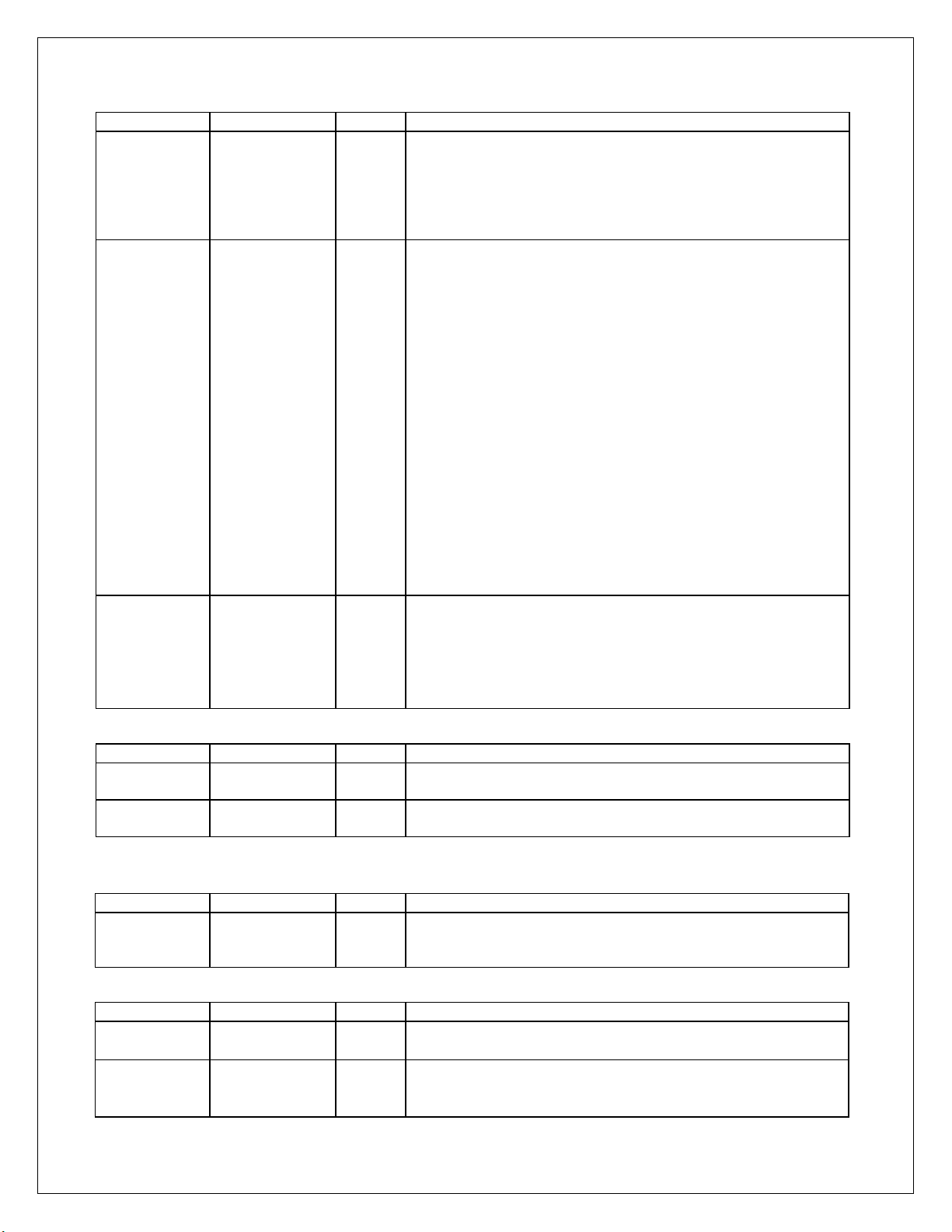
2.2 Pin Description
Note:
For those pins, which have multiple functions, pin name is separated by slash (“/”).
If not specified, all signals are default to digital signals.
Please refer to section ‘1.5.3 Pin Type Descriptions’ for an explanation of pin
abbreviations.
2.2.1 Twisted Pair Interface, 32 pins
Pin # Pin Name Type Description
123, 5, 7, 17
19, 29, 31, 41
124, 4, 8, 16
20, 28, 32, 40
126, 2, 10, 14
22, 26, 34, 38
127, 1, 11, 23
23, 25, 35, 37
TXP[0:7] O,
Analog
TXN[0:7] O,
Analog
RXP[0:7] I, Analog Twisted Pair Receive Input Positive.
RXN[0:7] I, Analog Twisted Pair Receive Input Negative.
Twisted Pair Transmit Output Positive.
Twisted Pair Transmit Output Negative.
2.2.2 Ground and Power, 20 pins
Pin # Pin Name Type Description
125, 3, 9, 15,
21, 27, 33, 39
118, 128, 12,
24, 36
122, 6, 18, 30,
42
120 GNDRCV Analog
121 VCCPLL2 Analog
GNDRT Analog
Ground
VCCAD Analog
Power
VCCA2 Analog
Power
Ground
Power
Analog Ground Pad
Analog 3.3V Power
Analog 1.8V Power
Analog Ground used by Clock Generator module
Analog 1.8V Power used by Clock Generator module
2.2.3 Mode Setting
Pin # Pin Name Type Description
43 RSMODE1 I, PD RMII and SMII/SS_SMII mode select signal. Dedicated input
provided by ADM7008 to determine the interface:
0: SMII or SS_SMII interface (See CRSDV_P6 power on setting
for more detail)
1: RMII interface
2.2.4 Clock Input Select
Pin # Pin Name Type Description
48 REFCLK_SEL I, PD XI/XO and REFCLK clock select signal. Dedicated input
provided by ADM7008 to determine the clock source for
ADM7008.
0: ADM7008 will use XI/XO as clock source for internal clock
generator. In this mode, REFCLK (pin 112) will output 50M
clock in RMII mode (RSMODE1 is set to 1) and 125M clock
in either SMII or SS_SMII mode (RSMODE1 is set to 0) \
1: ADM7008 will use the input of REFCLK (pin 112) as the
ADMtek Inc. 2-2

ADM7008 Interface Description
A
Pin # Pin Name Type Description
clock source for internal clock generator.
Note: that when RSMODE1 is set to 1 (RMII mode), the input
of REFCLK should be 50M; when RSMODE1 is set to 0
(SMII or SS_SMII mode) the clock input on REFCLK
should be 125M
2.2.5 Clock Input, 3 pins
Pin # Pin Name Type Pin Description
115 XI/OSCI I, CTL Crystal/Oscillator input.
REFCLK_SEL = 0: 25M Crystal/Oscillator Input.
REFCLK_SEL = 1: Leave unconnected
116 XO O, CTL Crystal output. When 25M Oscillator is used, this pin should be
left unconnected. See XI/OSCI description above.
111 REFCLK I/O,
16mA
LVTTL
Reference clock. Function on this pin is highly depended upon
the setting on REFCLK_SEL and RSMODE1:
REFCLK_SEL RSMODE1 REFCLK (Direction/Frequency)
0 0 Output/125 MHz
0 1 Output/50 MHz
1 0 Input/125 MHz with maximum 100ppm
1 1 Input/50 MHz with maximum 100ppm
2.2.6 RMII/SMII Interface, 48 pins
Pin # Pin Name Type Pin Description
51, 52 Power On
Setting
REC_10M_P7,
EN_AUTOMDIX
RMII Mode
RXD[1:0]_P7
SMII/SS_SMII
Mode
SPDLED_P7,
SMII_RXD_P7
I/O,
8mA,
PD/PU
REC_10M: Value on RXD1_P7 will be latched by ADM7008
during power on reset as Port 7 10M Re-command value.
0: Recommend Port 7 to operate in 100M Mode
1: Recommend Port 7 to operate in 10M Mode
ADM7008 during power on reset as Auto MDIX function control
signal.
0: Disable all ports’ Auto MDIX function.
1: Enable all ports’ Auto MDIX function.
Port 7 RMII Receive Data. RXD[1:0] are the port 7 output dibits synchronously to REFCLK. Upon assertion of CRSDV_P,
RXD0 and RXD1 remain at 00 until valid data is output from the
FIFO onto RXD. 01 on RXD1 and RXD0 indicates the start of
valid data. If a false carrier or a symbol error is detected, RXD1
and RXD0 are set to 10 for the duration of the activity. Note
that in 100Mb/s mode RXD can change once per REFCLK
cycle, whereas in 10Mb/s mode RXD must be held steady for
10 consecutive REFCLK cycles.
Port 7 SMII Receive Data. RXD0 for the designated port
outputs data or in-band management information
synchronously to SMII REFCLK (pin 70). In 100Mb/s mode,
RXD0 outputs a new 10-bit segment starting with SYNC. In
10Mb/s mode, RXD0 must repeat each 10 bits segment 10
times. RXD1 for the designated port is acted as Speed Status
LED for port 7.
uto MDIX Enable signal: Value on RXD0_P7 will be latched by
ADMtek Inc. 2-3

ADM7008 Interface Description
Pin # Pin Name Type Pin Description
SS_SMII Mode
SPDLED_P7,
SSS_SMII_RXD
_P7
53 Power On
Setting
FX_PAUSE
RMII Mode
CRSDV_P7
SMII/SS_SMII
Mode N/A
54, 55 RMII Mode
TXD[1:0]_P7
SMII Mode
LNKACT_P7,
SMII_TXD_P7
SMII Mode
LNKACT_P7,
SSSMII_TXD_P7
56 RMII Mode
TXEN_P7
SMII/SS_SMII
LOW
I, LVTTL,
O, 8mA
PD
I, TTL,
PD
I, TTL Port 7 Transmit Enable. Transmit Enable for port 7 indicates
Port 7 SS_SMII Receive Data. RXD0 for the designated port
outputs data or in-band management information
synchronously to RXCLK (pin 75). In 100Mb/s mode, RXD0
outputs a new 10-bit segment starting with SYNC. In 10Mb/s
mode, RXD0 must repeat each 10 bits segment 10 times.
RXD1 for the designated port is acted as Speed Status LED for
port 7.
Fiber PAUSE Recommend Value. Value on this pin will be
latched by ADM7008 during power on reset as Fiber port (See
SELFX power on setting for more detail) pause capability
control signal.
0: Pause off for all fiber ports
1: Pause on for all fiber ports
Port 7 Carrier Sense/Receive Data Valid. CRSDV_P7 asserts
when the receive medium is non-idle. The assertion of
CRSDV_P7 is asynchronous to REFCLK. At the de-assertion
of carrier, CRSDV_P7 de-asserts synchronously to REFCLK
only on the first di-bit of RXD. If there is still data in the FIFO
not yet presented onto RXD, then on the second di-bit of RXD,
CRSDV_P7 is asserted synchronously to REFCLK. The
toggling of CRSDV_P7 on the first and second di-bit continues
until all the data in the FIFO is presented onto RXD.
CRSDV_P7 is asserted for the duration of carrier activity for a
false carrier event.
Not used in SMII/SS_SMII Mode
Port 7 RMII Transmit Data. Transmit data for port 7 input the
di-bits that re transmitted and are driven synchronously to
REFCLK.
Note: that in 100Mb/s mode, TXD can change once per
REFCLK cycle, whereas in 10Mb/s mode, TXD must be held
steady for 10 consecutive REFCLK cycles.
Link and Activity LED/Port 7 SMII Transmit Data. TXD0 for port
7 inputs the data that is transmitted and is driven synchronously
to SMII_REFCLK (pin 70). In 100Mb/s mode, TXD0 inputs a
new 10-bit segment starting with SYNC. In 10Mb/s mode,
TXD0 must repeat each 10-bit segment 10 times. TXD1_P7
acts as Port 7 Link/Activity LED in both SMII and SS_SMII
Mode. See LED Description for more detail.
Link and Activity LED/Port 7 SS_SMII Transmit Data. TXD0 for
port 7 inputs the data that is transmitted and is driven
synchronously to TXCLK (pin 70). In 100Mb/s mode, TXD0
inputs a new 10-bit segment starting with SYNC. In 10Mb/s
mode, TXD0 must repeat each 10-bit segment 10 times.
that the di-bit on TXD is valid and it is driven synchronously to
REFCLK.
TIED TO LOW. TXEN_P7 should be tied to low for normal
operation.
ADMtek Inc. 2-4

ADM7008 Interface Description
Pin # Pin Name Type Pin Description
59, 60
61
Power On
Setting
REC_10M_P6,
DUALLED
RMII Mode
RXD[1:0]_P6
SMII Mode
SPDLED_P6,
SMII_RXD_P6
SS_SMII Mode
SPDLED_P6,
SSSMII_RXD_P
6
Power On
Setting
RSMODE0
RMII Mode
CRSDV_P6
PD,
PD,
8mA
8mA
8mA
LVTTL,
PD
8mA
REC_10M: Value on RXD1_P6 will be latched by ADM7008
I
during power on reset as Port 6 10M Re-command value.
0: Recommend Port 6 to operate in 100M Mode
1: Recommend Port 6 to operate in 10M Mode
Dual Color LED Mode. Value on RXD0_P6 will be latched by
ADM7008 during power on reset to form LED control signal.
Value on this pin will affect the output value on Serial LED
output.
0: Single Color 3 bits/port serial stream (Default Value)
1: Dual Color 3 bits/port serial stream
Port 6 RMII Receive Data. RXD[1:0] are the port 6 output di-
O,
bits synchronously to REFCLK. Upon assertion of CRSDV_P,
RXD0 and RXD1 remain at 00 until valid data is output from the
FIFO onto RXD. The start of valid data is indicated by 01 on
RXD1 and RXD0. If a false carrier or a symbol error is
detected, RXD1 and RXD0 are set to 10 for the duration of the
activity. Note that in 100Mb/s mode RXD can change once per
REFCLK cycle, whereas in 10Mb/s mode RXD must be held
steady for 10 consecutive REFCLK cycles.
Port 6 SMII Receive Data. RXD0 for the designated port
O,
outputs data or in-band management information
synchronously to SMII REFCLK (pin 70). In 100Mb/s mode,
RXD0 outputs a new 10-bit segment starting with SYNC. In
10Mb/s mode, RXD0 must repeat each 10 bits segment 10
times. RXD1 for the designated port is acted as Speed Status
LED for port 6.
Port 6 SS_SMII Receive Data. RXD0 for the designated port
O,
outputs data or in-band management information
synchronously to RXCLK (pin 75). In 100Mb/s mode, RXD0
outputs a new 10-bit segment starting with SYNC. In 10Mb/s
mode, RXD0 must repeat each 10 bits segment 10 times.
RXD1 for the designated port is acted as Speed Status LED for
port 6.
RMII/SMII/SS_SMII Configuration bit 0. Value on this pin will
I,
be latched by ADM7008 during power on reset as interface
configuration bit 0. Combined with RSMODE1 (pin 43), three
possible interfaces are provided by ADM7008
RSMODE[1:0] Interface
00 SMII
01 SS_SMII
1x RMII
Port 6 Carrier Sense/Receive Data Valid. CRSDV_P6 asserts
O,
when the receive medium is non-idle. The assertion of
CRSDV_P6 is asynchronous to REFCLK. At the de-assertion
of carrier, CRSDV_P6 de-asserts synchronously to REFCLK
only on the first di-bit of RXD. If there is still data in the FIFO
not yet presented onto RXD, then on the second di-bit of RXD,
ADMtek Inc. 2-5

ADM7008 Interface Description
g
Pin # Pin Name Type Pin Description
62, 63
64
65, 66
SMII/SS_SMII
Mode
N/A
RMII Mode
TXD[1:0]_P6
SMII Mode
LNKACT_P6,
SMII_TXD_P6
SS_SMII Mode
LNKACT_P6,
SSSMII_TXD_P6
RMII Mode
TXEN_P6
SMII/SS_SMII
LOW
Power On
Setting
REC_10M_P5,
PWSAVE_DIS
RMII Mode
RXD[1:0]_P5
LVTTL,
PD,
PD
TTL
I,
PD,
PD
O,
8mA
CRSDV_P6 is asserted synchronously to REFCLK. The
toggling of CRSDV_P6 on the first and second di-bit continues
until all the data in the FIFO is presented onto RXD.
CRSDV_P6 is asserted for the duration of carrier activity for a
false carrier event.
Not Used.
Not used in SMII/SS_SMII Mode
I,
Port 6 RMII Transmit Data. Transmit data for port 6 input the
di-bits that re transmitted and are driven synchronously to
REFCLK. Note that in 100Mb/s mode, TXD can change once
per REFCLK cycle, whereas in 10Mb/s mode, TXD must be
held steady for 10 consecutive REFCLK cycles.
Link and Activity LED/Port 6 SMII Transmit Data. TXD0 for port
6 inputs the data that is transmitted and is driven synchronously
to SMII_REFCLK (pin 70). In 100Mb/s mode, TXD0 inputs a
new 10-bit segment starting with SYNC. In 10Mb/s mode,
TXD0 must repeat each 10-bit segment 10 times.
TXD1_P6 acts as Port 6 Link/Activity LED in both SMII and
SS_SMII Mode. See LED Description for more detail.
Link and Activity LED/Port 6 SS_SMII Transmit Data. TXD0 for
port 6 inputs the data that is transmitted and is driven
synchronously to TXCLK (pin 70). In 100Mb/s mode, TXD0
inputs a new 10-bit segment starting with SYNC. In 10Mb/s
mode, TXD0 must repeat each 10-bit segment 10 times.
I,
Port 6 Transmit Enable. Transmit Enable for port 6 indicates
that the di-bit on TXD is valid and it is driven synchronously to
REFCLK.
TIED TO LOW. TXEN_P6 should be tied to low for normal
operation in both SMII and SS_SMII Mode.
REC_10M: Value on RXD1_P5 will be latched by ADM7008
during power on reset as Port 5 10M Re-command value.
0: Recommend Port 5 to operate in 100M Mode (Default)
1: Recommend Port 5 to operate in 10M Mode
Lower power Link Pulse Function (Power Saving, LLP) Disable.
Value on RXD1 will be latched by ADM7008 during power on
reset as power saving disable signal. (See Lower Power Link
Pulse Function description for more detail)
0: Power Saving Enable
1: Power Saving disable (Default)
Port 5 RMII Receive Data. RXD[1:0] are the port 5 output dibits synchronously to REFCLK. Upon assertion of CRSDV_P,
RXD0 and RXD1 remain at 00 until valid data is output from the
FIFO onto RXD. 01 on RXD1 and RXD0 indicates the start of
valid data. If a false carrier or a symbol error is detected, RXD1
and RXD0 are set to 10 for the duration of the activity. Note
that in 100Mb/s mode RXD can chan
e once per REFCLK
ADMtek Inc. 2-6

ADM7008 Interface Description
Pin # Pin Name Type Pin Description
67
68, 69
SMII Mode
SPDLED_P5,
SMII_RXD_P5
SS_SMII Mode
SPDLED_P5,
SSSMII_RXD_P
5
Power On
Setting
TP_PAUSE
RMII Mode
CRSDV_P5
SMII/SS_SMII
Mode
N/A
RMII Mode
TXD[1:0]_P5
SMII Mode
LNKACT_P5,
SMII_TXD_P5
LVTTL,
PU
8mA
TTL,
PD
cycle, whereas in 10Mb/s mode RXD must be held steady for
10 consecutive REFCLK cycles.
Port 5 SMII Receive Data. RXD0 for the designated port
outputs data or in-band management information
synchronously to SMII REFCLK (pin 70). In 100Mb/s mode,
RXD0 outputs a new 10-bit segment starting with SYNC. In
10Mb/s mode, RXD0 must repeat each 10 bits segment 10
times. RXD1 for the designated port is acted as Speed Status
LED for port 5.
Port 5 SS_SMII Receive Data. RXD0 for the designated port
outputs data or in-band management information
synchronously to RXCLK (pin 75). In 100Mb/s mode, RXD0
outputs a new 10-bit segment starting with SYNC. In 10Mb/s
mode, RXD0 must repeat each 10 bits segment 10 times.
RXD1 for the designated port is acted as Speed Status LED for
port 5.
I,
Twisted Pair PAUSE Recommend Value. Value on this pin will
be latched by ADM7008 during power on reset as twisted pair
port (See SELFX power on setting for more detail) pause
capability control signal.
0: Pause off for all twisted pair ports
1: Pause on for all twisted pair ports
O,
Port 5 Carrier Sense/Receive Data Valid. CRSDV_P5 asserts
when the receive medium is non-idle. The assertion of
CRSDV_P5 is asynchronous to REFCLK. At the de-assertion
of carrier, CRSDV_P5 de-asserts synchronously to REFCLK
only on the first di-bit of RXD. If there is still data in the FIFO
not yet presented onto RXD, then on the second di-bit of RXD,
CRSDV_P5 is asserted synchronously to REFCLK. The
toggling of CRSDV_P5 on the first and second di-bit continues
until all the data in the FIFO is presented onto RXD.
CRSDV_P5 is asserted for the duration of carrier activity for a
false carrier event.
Not Used.
Not used in SMII/SS_SMII Mode
I,
Port 5 RMII Transmit Data. Transmit data for port 5 inputs the
di-bits that re transmitted and are driven synchronously to
REFCLK. Note that in 100Mb/s mode, TXD can change once
per REFCLK cycle, whereas in 10Mb/s mode, TXD must be
held steady for 10 consecutive REFCLK cycles.
Link and Activity LED/Port 5 SMII Transmit Data. TXD0 for port
5 inputs the data that is transmitted and is driven synchronously
to SMII_REFCLK (pin 70). In 100Mb/s mode, TXD0 inputs a
new 10-bit segment starting with SYNC. In 10Mb/s mode,
TXD0 must repeat each 10-bit segment 10 times.
TXD1_P5 acts as Port 5 Link/Activity LED in both SMII and
SS_SMII Mode. See LED Description for more detail.
ADMtek Inc. 2-7

ADM7008 Interface Description
Pin # Pin Name Type Pin Description
70
73, 74
75
SS_SMII Mode
LNKACT_P5,
SSSMII_TXD_P5
RMII Mode
TXEN_P5
SMII/SS_SMII
LOW
Power On
Setting
REC_10M_P4,
TP_DUPLEX
RMII Mode
RXD[1:0]_P4
SMII Mode
SPDLED_P4,
SMII_RXD_P4
SS_SMII Mode
SPDLED_P4,
SSSMII_RXD_P
4
Power On
Setting
DLY2NS
TTL
I/O,
8mA,
PD/PU
LVTTL,
PD
Link and Activity LED/Port 5 SS_SMII Transmit Data. TXD0 for
port 5 inputs the data that is transmitted and is driven
synchronously to TXCLK (pin 70). In 100Mb/s mode, TXD0
inputs a new 10-bit segment starting with SYNC. In 10Mb/s
mode, TXD0 must repeat each 10-bit segment 10 times.
I,
Port 5 Transmit Enable. Transmit Enable for port 5 indicates
that the di-bit on TXD is valid and it is driven synchronously to
REFCLK.
SMII/SS_SMII Mode. Keep LOW for normal operation.
REC_10M: Value on RXD1_P4 will be latched by ADM7008
during power on reset as Port 4 10M Re-command value.
0: Recommend Port 4 to operate in 100M Mode
1: Recommend Port 4 to operate in 10M Mode
Twisted Pair Duplex Recommend Value. Value on RXD1 will
be latched by ADM7008 during power on reset as duplex
recommend value for twisted pair interface.
0: Half Duplex for all twisted pair ports
1: Full Duplex for all twisted pair ports
Port 4 RMII Receive Data. RXD[1:0] are the port 4 output dibits synchronously to REFCLK. Upon assertion of CRSDV_P,
RXD0 and RXD1 remain at 00 until valid data is output from the
FIFO onto RXD. 01 on RXD1 and RXD0 indicates the start of
valid data. If a false carrier or a symbol error is detected, RXD1
and RXD0 are set to 10 for the duration of the activity. Note
that in 100Mb/s mode RXD can change once per REFCLK
cycle, whereas in 10Mb/s mode RXD must be held steady for
10 consecutive REFCLK cycles.
Port 4 SMII Receive Data. RXD0 for the designated port
outputs data or in-band management information
synchronously to SMII REFCLK (pin 70). In 100Mb/s mode,
RXD0 outputs a new 10-bit segment starting with SYNC. In
10Mb/s mode, RXD0 must repeat each 10 bits segment 10
times. RXD1 for the designated port is acted as Speed Status
LED for port 4.
Port 4 SS_SMII Receive Data. RXD0 for the designated port
outputs data or in-band management information
synchronously to RXCLK (pin 75). In 100Mb/s mode, RXD0
outputs a new 10-bit segment starting with SYNC. In 10Mb/s
mode, RXD0 must repeat each 10 bits segment 10 times.
RXD1 for the designated port is acted as Speed Status LED for
port 4.
I,
REFCLK Delay 2ns. Value on this pin will be latched by
ADM7008 during power on reset as delay select signal for
REFCLK input when REFCLK_SEL and RSMODE1 are both
set to 1 (RMII interface with REFCLK as clock input)
ADMtek Inc. 2-8

ADM7008 Interface Description
/
Pin # Pin Name Type Pin Description
76, 77
78
RMII Mode
CRSDV_P4
SMII Mode
N/A
SS_SMII Mode
RXCLK
RMII Mode
TXD[1:0]_P4
SMII Mode
LNKACT_P4,
SMII_TXD_P4
SS_SMII Mode
LNKACT_P4,
SSSMII_TXD_P4
RMII Mode
TXEN_P4
SMII Mode
SMII_REFCLK
O,
8mA
I,
TTL,
PD
I,
TTL
0: Normal REFCLK clock path
1: REFCLK delay by 2 ns
Port 4 Carrier Sense/Receive Data Valid. CRSDV_P4 asserts
when the receive medium is non-idle. The assertion of
CRSDV_P4 is asynchronous to REFCLK. At the de-assertion
of carrier, CRSDV_P4 de-asserts synchronously to REFCLK
only on the first di-bit of RXD. If there is still data in the FIFO
not yet presented onto RXD, then on the second di-bit of RXD,
CRSDV_P4 is asserted synchronously to REFCLK. The
toggling of CRSDV_P4 on the first and second di-bit continues
until all the data in the FIFO is presented onto RXD.
CRSDV_P4 is asserted for the duration of carrier activity for a
false carrier event.
Not Used.
Not used in SMII Mode
125M Receive Clock. This pin acts as 125M receive clock
when ADM7008 is programmed to SS_SMII mode. All
SSS_SMII_RXD are synchronous to the rising edge of this
clock.
Note: that clock on this pin will not be active during power on
reset due to power on setting.
Port 4 RMII Transmit Data. Transmit data for port 4 inputs the
di-bits that re transmitted and are driven synchronously to
REFCLK. Note that in 100Mb/s mode, TXD can change once
per REFCLK cycle, whereas in 10Mb/s mode, TXD must be
held steady for 10 consecutive REFCLK cycles.
Link and Activity LED
4 inputs the data that is transmitted and is driven synchronously
to SMII_REFCLK (pin 70). In 100Mb/s mode, TXD0 inputs a
new 10-bit segment starting with SYNC. In 10Mb/s mode,
TXD0 must repeat each 10-bit segment 10 times.
TXD1_P4 acts as Port 4 Link/Activity LED in both SMII and
SS_SMII Mode. See LED Description for more detail.
Link and Activity LED/Port 4 SS_SMII Transmit Data. TXD0 for
port 4 inputs the data that is transmitted and is driven
synchronously to TXCLK (pin 70). In 100Mb/s mode, TXD0
inputs a new 10-bit segment starting with SYNC. In 10Mb/s
mode, TXD0 must repeat each 10-bit segment 10 times.
Port 4 Transmit Enable. Transmit Enable for port 4 indicates
that the di-bit on TXD is valid and it is driven synchronously to
REFCLK.
SMII 125M Reference Clock. In SMII Mode, this pin acts as
125M reference clock for all ports. All transmit and receive data
(include transmit enable and receive data valid) should be
synchronous to the rising edge of this clock.
Port 4 SMII Transmit Data. TXD0 for port
ADMtek Inc. 2-9

ADM7008 Interface Description
Pin # Pin Name Type Pin Description
81, 82
83
SS_SMII Mode
TXCLK
Power On
Setting
REC_10M_P3,
ANENDIS
RMII Mode
RXD[1:0]_P3
SMII Mode
SPDLED_P3,
SMII_RXD_P3
SS_SMII Mode
SPDLED_P3,
SSSMII_RXD_P
3
Power On
Setting
TESTSEL2
RMII Mode
CRSDV_P3
I/O,
8mA,
PD
PD
8mA
SS_SMII 125M Transmit Clock. In SS_SMII Mode, this pin acts
as 125M transmit clock for all ports. TXD and TXEN should be
synchronous to the rising edge of this clock.
REC_10M: Value on RXD1_P3 will be latched by ADM7008
during power on reset as Port 3 10M Re-command value.
0: Recommend Port 3 to operate in 100M Mode
1: Recommend Port 3 to operate in 10M Mode
Twisted Pair Duplex Recommend Value. Value on RXD1 will
be latched by ADM7008 during power on reset as auto
negotiation disable recommend value for twisted pair interface.
0: Auto-negotiation Enable for all twisted pair ports.
1: Auto-negotiation Disable for all twisted pair ports
Port 3 RMII Receive Data. RXD[1:0] are the port 3 output dibits synchronously to REFCLK. Upon assertion of CRSDV_P,
RXD0 and RXD1 remain at 00 until valid data is output from the
FIFO onto RXD. The start of valid data is indicated by 01 on
RXD1 and RXD0. If a false carrier or a symbol error is
detected, RXD1 and RXD0 are set to 10 for the duration of the
activity. Note that in 100Mb/s mode RXD can change once per
REFCLK cycle, whereas in 10Mb/s mode RXD must be held
steady for 10 consecutive REFCLK cycles.
Port 3 SMII Receive Data. RXD0 for the designated port
outputs data or in-band management information
synchronously to SMII REFCLK (pin 70). In 100Mb/s mode,
RXD0 outputs a new 10-bit segment starting with SYNC. In
10Mb/s mode, RXD0 must repeat each 10 bits segment 10
times. RXD1 for the designated port is acted as Speed Status
LED for port 3.
Port 3 SS_SMII Receive Data. RXD0 for the designated port
outputs data or in-band management information
synchronously to RXCLK (pin 75). In 100Mb/s mode, RXD0
outputs a new 10-bit segment starting with SYNC. In 10Mb/s
mode, RXD0 must repeat each 10 bits segment 10 times.
RXD1 for the designated port is acted as Speed Status LED for
port 3.
I,
Industrial Test Mode Select 2. Value on this pin will be latched
by ADM7008 during power on reset as industrial test mode
select bit 2. Pull down for normal operation. For Test Mode,
See test select 0 for more detail
O,
Port 3 Carrier Sense/Receive Data Valid. CRSDV_P3 asserts
when the receive medium is non-idle. The assertion of
CRSDV_P3 is asynchronous to REFCLK. At the de-assertion
of carrier, CRSDV_P3 de-asserts synchronously to REFCLK
only on the first di-bit of RXD. If there is still data in the FIFO
not yet presented onto RXD, then on the second di-bit of RXD,
CRSDV_P3 is asserted synchronously to REFCLK. The
toggling of CRSDV_P3 on the first and second di-bit continues
ADMtek Inc. 2-10

ADM7008 Interface Description
Pin # Pin Name Type Pin Description
84, 85
86
89, 90
SMII Mode
N/A
SS_SMII Mode
RX_SYNC
RMII Mode
TXD[1:0]_P3
SMII Mode
LNKACT_P3,
SMII_TXD_P3
SS_SMII Mode
LNKACT_P3,
SSSMII_TXD_P3
RMII Mode
TXEN_P3
SMII Mode
SMII_SYNC
SS_SMII Mode
TX_SYNC
Power On
Setting
REC_10M_P2,
PHYADDR0
RMII Mode
RXD[1:0]_P2
TTL,
PD
TTL
PD,
PD
8mA
until all the data in the FIFO is presented onto RXD.
CRSDV_P3 is asserted for the duration of carrier activity for a
false carrier event.
Not Used.
Not used in SMII Mode
SS_SMII Receive Synchronization Signal. In SS_SMII Mode,
this pin sets the bit stream alignment of SSS_SMII_RXD for all
ports.
I,
Port 3 RMII Transmit Data. Transmit data for port 3 inputs the
di-bits that re transmitted and are driven synchronously to
REFCLK. Note that in 100Mb/s mode, TXD can change once
per REFCLK cycle, whereas in 10Mb/s mode, TXD must be
held steady for 10 consecutive REFCLK cycles.
Link and Activity LED/Port 3 SMII Transmit Data. TXD0 for port
3 inputs the data that is transmitted and is driven synchronously
to SMII_REFCLK (pin 70). In 100Mb/s mode, TXD0 inputs a
new 10-bit segment starting with SYNC. In 10Mb/s mode,
TXD0 must repeat each 10-bit segment 10 times.
TXD1_P3 acts as Port 3 Link/Activity LED in both SMII and
SS_SMII Mode. See LED Description for more detail.
Link and Activity LED/Port 3 SS_SMII Transmit Data. TXD0 for
port 3 inputs the data that is transmitted and is driven
synchronously to TXCLK (pin 70). In 100Mb/s mode, TXD0
inputs a new 10-bit segment starting with SYNC. In 10Mb/s
mode, TXD0 must repeat each 10-bit segment 10 times.
I,
Port 3 Transmit Enable. Transmit Enable for port 3 indicates
that the di-bit on TXD is valid and it is driven synchronously to
REFCLK.
SMII Synchronization Signal. In SMII Mode, this pin sets the bit
stream alignment of SMII_TXD and SMII_RXD for all ports.
SS_SMII Transmit Synchronization Signal. In SS_SMII Mode,
this pin sets the bit stream alignment of SSS_SMII_TXD for all
ports.
REC_10M: Value on RXD1_P2 will be latched by ADM7008
I,
during power on reset as Port 2 10M Re-command value.
0: Recommend Port 2 to operate in 100M Mode (100M)
1: Recommend Port 2 to operate in 10M Mode
PHY Address Bit 0. Value on RXD1 will be latched by
ADM7008 during power on reset as PHY address bit 0.
Combined with PHYADDR1 (pin 44) to form PHY address for
ADM7008. See PHYADDR1 description for more detail
Port 2 RMII Receive Data. RXD[1:0] are the port 2 output di-
O,
bits synchronously to REFCLK. Upon assertion of CRSDV_P,
RXD0 and RXD1 remain at 00 until valid data is output from the
ADMtek Inc. 2-11

ADM7008 Interface Description
Pin # Pin Name Type Pin Description
91
92, 93
SMII Mode
SPDLED_P2,
SMII_RXD_P2
SS_SMII Mode
SPDLED_P2,
SSSMII_RXD_P
2
Power On
Setting
FX_DUPLEX
RMII Mode
CRSDV_P2
SMII/SS_SMII
Mode
N/A
RMII Mode
TXD[1:0]_P2
SMII Mode
LNKACT_P2,
SMII_TXD_P2
I/O,
8mA
PU
TTL,
PD
FIFO onto RXD. The start of valid data is indicated by 01 on
RXD1 and RXD0. If a false carrier or a symbol error is
detected, RXD1 and RXD0 are set to 10 for the duration of the
activity. Note that in 100Mb/s mode RXD can change once per
REFCLK cycle, whereas in 10Mb/s mode RXD must be held
steady for 10 consecutive REFCLK cycles.
Port 2 SMII Receive Data. RXD0 for the designated port
outputs data or in-band management information
synchronously to SMII REFCLK (pin 70). In 100Mb/s mode,
RXD0 outputs a new 10-bit segment starting with SYNC. In
10Mb/s mode, RXD0 must repeat each 10 bits segment 10
times. RXD1 for the designated port is acted as Speed Status
LED for port 2.
Port 2 SS_SMII Receive Data. RXD0 for the designated port
outputs data or in-band management information
synchronously to RXCLK (pin 75). In 100Mb/s mode, RXD0
outputs a new 10-bit segment starting with SYNC. In 10Mb/s
mode, RXD0 must repeat each 10 bits segment 10 times.
RXD1 for the designated port is acted as Speed Status LED for
port 2.
Duplex Recommend Value for Fiber Port. Value on this pin will
be latched by ADM7008 during power on reset as duplex
recommend value for all fiber ports.
0: Half duplex for all fiber ports.
1: Full duplex for all fiber ports.
Port 2 Carrier Sense/Receive Data Valid. CRSDV_P2 asserts
when the receive medium is non-idle. The assertion of
CRSDV_P2 is asynchronous to REFCLK. At the de-assertion
of carrier, CRSDV_P2 de-asserts synchronously to REFCLK
only on the first di-bit of RXD. If there is still data in the FIFO
not yet presented onto RXD, then on the second di-bit of RXD,
CRSDV_P2 is asserted synchronously to REFCLK. The
toggling of CRSDV_P2 on the first and second di-bit continues
until all the data in the FIFO is presented onto RXD.
CRSDV_P2 is asserted for the duration of carrier activity for a
false carrier event.
Not Used.
Not used in SMII and SS_SMII Mode
I,
Port 2 RMII Transmit Data. Transmit data for port 2 inputs the
di-bits that re transmitted and are driven synchronously to
REFCLK. Note that in 100Mb/s mode, TXD can change once
per REFCLK cycle, whereas in 10Mb/s mode, TXD must be
held steady for 10 consecutive REFCLK cycles.
Link and Activity LED/Port 2 SMII Transmit Data. TXD0 for port
2 inputs the data that is transmitted and is driven synchronously
to SMII_REFCLK (pin 70). In 100Mb/s mode, TXD0 inputs a
ADMtek Inc. 2-12

ADM7008 Interface Description
Pin # Pin Name Type Pin Description
94
95, 96
97
SS_SMII Mode
LNKACT_P2,
SSSMII_TXD_P2
RMII Mode
TXEN_P2
SMII/SS_SMII
LOW
Power On
Setting
REC_10M_P1,
TESTSEL1
RMII Mode
RXD[1:0]_P1
SMII Mode
SPDLED_P1,
SMII_RXD_P1
SS_SMII Mode
SPDLED_P1,
SSSMII_RXD_P
1
Power On
TTL
I/O,
8mA,
PD
I/O, Fiber/Twisted Pair Configuration bit 1. Value on RXD1 will be
new 10-bit segment starting with SYNC. In 10Mb/s mode,
TXD0 must repeat each 10-bit segment 10 times.
TXD1_P2 acts as Port 2 Link/Activity LED in both SMII and
SS_SMII Mode. See LED Description for more detail.
Link and Activity LED/Port 2 SS_SMII Transmit Data. TXD0 for
port 2 inputs the data that is transmitted and is driven
synchronously to TXCLK (pin 70). In 100Mb/s mode, TXD0
inputs a new 10-bit segment starting with SYNC. In 10Mb/s
mode, TXD0 must repeat each 10-bit segment 10 times.
I,
Port 2 Transmit Enable. Transmit Enable for port 2 indicates
that the di-bit on TXD is valid and it is driven synchronously to
REFCLK.
Not Used. Tied to LOW for normal operation in SMII/SS_SMII
mode.
REC_10M: Value on RXD1_P1 will be latched by ADM7008
during power on reset as Port 1 10M Re-command value.
0: Recommend Port 1 to operate in 100M Mode
1: Recommend Port 1 to operate in 10M Mode
Industrial Test Mode Select 1. Value on RXD0_P1 will be
latched by ADM7008 during power on reset as industrial test
mode select bit 1. Pull down for normal operation. For Test
Mode, See test select 0 for more detail
Port 1 RMII Receive Data. RXD[1:0] are the port 1 output dibits synchronously to REFCLK. Upon assertion of CRSDV_P,
RXD0 and RXD1 remain at 00 until valid data is output from the
FIFO onto RXD. The start of valid data is indicated by 01 on
RXD1 and RXD0. If a false carrier or a symbol error is
detected, RXD1 and RXD0 are set to 10 for the duration of the
activity. Note that in 100Mb/s mode RXD can change once per
REFCLK cycle, whereas in 10Mb/s mode RXD must be held
steady for 10 consecutive REFCLK cycles.
Port 1 SMII Receive Data. RXD0 for the designated port
outputs data or in-band management information
synchronously to SMII REFCLK (pin 70). In 100Mb/s mode,
RXD0 outputs a new 10-bit segment starting with SYNC. In
10Mb/s mode, RXD0 must repeat each 10 bits segment 10
times. RXD1 for the designated port is acted as Speed Status
LED for port 1.
Port 1 SS_SMII Receive Data. RXD0 for the designated port
outputs data or in-band management information
synchronously to RXCLK (pin 75). In 100Mb/s mode, RXD0
outputs a new 10-bit segment starting with SYNC. In 10Mb/s
mode, RXD0 must repeat each 10 bits segment 10 times.
RXD1 for the designated port is acted as Speed Status LED for
port 1.
ADMtek Inc. 2-13

ADM7008 Interface Description
Pin # Pin Name Type Pin Description
98, 99
100
Setting
SELFX1
RMII Mode
CRSDV_P1
SMII/SS_SMII
Mode
N/A
RMII Mode
TXD[1:0]_P1
SMII Mode
LNKACT_P1,
SMII_TXD_P1
SS_SMII Mode
LNKACT_P1,
SSSMII_TXD_P1
RMII Mode
TXEN_P1
SMII/SS_SMII
LOW
8mA
PD
I,
TTL,
PD
I,
TTL
latched by ADM7008 during power on reset as fiber/twisted pair
interface configuration bit 1. Combined with SELFX0 (Power
On setting value on RXD0_P0) to program ADM7008 into 4
different modes.
00: all ports are twisted ports
01: only port 7 is fiber port, and all the other ports are twisted
ports.
10: only port 7 and port 6 are fiber ports, and all the other port
are twisted
port
11: all ports are fiber ports.
Port 1 Carrier Sense/Receive Data Valid. CRSDV_P1 asserts
when the receive medium is non-idle. The assertion of
CRSDV_P1 is asynchronous to REFCLK. At the de-assertion
of carrier, CRSDV_P1 de-asserts synchronously to REFCLK
only on the first di-bit of RXD. If there is still data in the FIFO
not yet presented onto RXD, then on the second di-bit of RXD,
CRSDV_P1 is asserted synchronously to REFCLK. The
toggling of CRSDV_P1 on the first and second di-bit continues
until all the data in the FIFO is presented onto RXD.
CRSDV_P1 is asserted for the duration of carrier activity for a
false carrier event.
Not Used.
Not used in SMII and SS_SMII Mode
Port 1 RMII Transmit Data. Transmit data for port 1 inputs the
di-bits that re transmitted and are driven synchronously to
REFCLK. Note that in 100Mb/s mode, TXD can change once
per REFCLK cycle, whereas in 10Mb/s mode, TXD must be
held steady for 10 consecutive REFCLK cycles.
Link and Activity LED/Port 1 SMII Transmit Data. TXD0 for port
1 inputs the data that is transmitted and is driven synchronously
to SMII_REFCLK (pin 70). In 100Mb/s mode, TXD0 inputs a
new 10-bit segment starting with SYNC. In 10Mb/s mode,
TXD0 must repeat each 10-bit segment 10 times.
TXD1_P1 acts as Port 1 Link/Activity LED in both SMII and
SS_SMII Mode. See LED Description for more detail.
Link and Activity LED/Port 1 SS_SMII Transmit Data. TXD0 for
port 1 inputs the data that is transmitted and is driven
synchronously to TXCLK (pin 70). In 100Mb/s mode, TXD0
inputs a new 10-bit segment starting with SYNC. In 10Mb/s
mode, TXD0 must repeat each 10-bit segment 10 times.
Port 1 Transmit Enable. Transmit Enable for port 1 indicates
that the di-bit on TXD is valid and it is driven synchronously to
REFCLK.
Not Used. Tied to LOW for normal operation in SMII/SS_SMII
mode.
ADMtek Inc. 2-14

ADM7008 Interface Description
Pin # Pin Name Type Pin Description
105, 106
107
Power On
Setting
REC_10M_P0,
TESTSEL0
RMII Mode
RXD[1:0]_P0
SMII Mode
SPDLED_P0,
SMII_RXD_P0
SS_SMII Mode
SPDLED_P0,
SSSMII_RXD_P
0
Power On
Setting
SELFX0
RMII Mode
CRSDV_P0
I/O,
8mA,
PD
I/O,
8mA
PD
REC_10M: Value on RXD1_P0 will be latched by ADM7008
during power on reset as Port 0 10M Re-command value.
0: Recommend Port 0 to operate in 100M Mode
1: Recommend Port 0 to operate in 10M Mode
Industrial Test Mode Select 0. Value on RXD0_P1 will be
latched by ADM7008 during power on reset as industrial test
mode select bit 0. Pull down TESTSEL[2:0] for normal
operation.
TESTSEL Mode
000: Normal Mode
Port 0 RMII Receive Data. RXD[1:0] are the port 0 output dibits synchronously to REFCLK. Upon assertion of CRSDV_P,
RXD0 and RXD1 remain at 00 until valid data is output from the
FIFO onto RXD. The start of valid data is indicated by 01 on
RXD1 and RXD0. If a false carrier or a symbol error is
detected, RXD1 and RXD0 are set to 10 for the duration of the
activity. Note that in 100Mb/s mode RXD can change once per
REFCLK cycle, whereas in 10Mb/s mode RXD must be held
steady for 10 consecutive REFCLK cycles.
Port 0 SMII Receive Data. RXD0 for the designated port
outputs data or in-band management information
synchronously to SMII REFCLK (pin 70). In 100Mb/s mode,
RXD0 outputs a new 10-bit segment starting with SYNC. In
10Mb/s mode, RXD0 must repeat each 10 bits segment 10
times. RXD1 for the designated port is acted as Speed Status
LED for port 0.
Port 0 SS_SMII Receive Data. RXD0 for the designated port
outputs data or in-band management information
synchronously to RXCLK (pin 75). In 100Mb/s mode, RXD0
outputs a new 10-bit segment starting with SYNC. In 10Mb/s
mode, RXD0 must repeat each 10 bits segment 10 times.
RXD1 for the designated port is acted as Speed Status LED for
port 0.
Fiber/Twisted Pair Configuration bit 0. Value on RXD1 will be
latched by ADM7008 during power on reset as fiber/twisted pair
interface configuration bit 1. Combined with SELFX1 (Power
On setting value on RXD0_P1) to program ADM7008 into 4
different modes. See SELFX1 for more detail
Port 0 Carrier Sense/Receive Data Valid. CRSDV_P0 asserts
when the receive medium is non-idle. The assertion of
CRSDV_P0 is asynchronous to REFCLK. At the de-assertion
of carrier, CRSDV_P0 de-asserts synchronously to REFCLK
only on the first di-bit of RXD. If there is still data in the FIFO
not yet presented onto RXD, then on the second di-bit of RXD,
CRSDV_P0 is asserted synchronously to REFCLK. The
toggling of CRSDV_P0 on the first and second di-bit continues
until all the data in the FIFO is presented onto RXD.
ADMtek Inc. 2-15
ADM7008 Interface Description
p
Pin # Pin Name Type Pin Description
108, 109
110
SMII/SS_SMII
Mode
N/A
RMII Mode
TXD[1:0]_P0
SMII Mode
LNKACT_P0,
SMII_TXD_P0
SS_SMII Mode
LNKACT_P0,
SSSMII_TXD_P0
RMII Mode
TXEN_P0
SMII/SS_SMII
LOW
TTL,
PD
TTL
CRSDV_P0 is asserted for the duration of carrier activity for a
false carrier event.
Not Used.
Not used in SMII and SS_SMII Mode
I,
Port 0 RMII Transmit Data. Transmit data for port 1 inputs the
di-bits that re transmitted and are driven synchronously to
REFCLK. Note that in 100Mb/s mode, TXD can change once
per REFCLK cycle, whereas in 10Mb/s mode, TXD must be
held steady for 10 consecutive REFCLK cycles.
Link and Activity LED/Port 0 SMII Transmit Data. TXD0 for port
0 inputs the data that is transmitted and is driven synchronously
to SMII_REFCLK (pin 70). In 100Mb/s mode, TXD0 inputs a
new 10-bit segment starting with SYNC. In 10Mb/s mode,
TXD0 must repeat each 10-bit segment 10 times.
TXD1_P0 acts as Port 0 Link/Activity LED in both SMII and
SS_SMII Mode. See LED Description for more detail.
Link and Activity LED/Port 0 SS_SMII Transmit Data. TXD0 for
port 1 inputs the data that is transmitted and is driven
synchronously to TXCLK (pin 70). In 100Mb/s mode, TXD0
inputs a new 10-bit segment starting with SYNC. In 10Mb/s
mode, TXD0 must repeat each 10-bit segment 10 times.
I,
Port 0 Transmit Enable. Transmit Enable for port 0 indicates
that the di-bit on TXD is valid and it is driven synchronously to
REFCLK.
Not Used. Tied to LOW for normal operation in SMII/SS_SMII
mode.
2.2.7 ATPG Signals, 2 pins
Pin # Pin Name Type Description
114 SCAN_EN I
VLTTL
113 SCAN_MODE I
VLTTL
SCAN_EN: Scan enable for test 0: Normal mode
SCAN_MODE: Scan mode select for test 0: Normal mode
2.2.8 Reset Pin
Pin # Pin Name Type Description
47 RESET# I,
SCHE
Reset Signal. Active low to bring ADM7008 into reset
condition. Recommend keeping low for at least 200 ms to
ensure the stability of the system after power on reset.
2.2.9 Control Signals, 3 pins
Pin # Pin Name Type Pin Description
101 MDIO I/O,
LVTTL
102 MDC I,
LVTTL
Management Data. MDIO transfers management data in and
out of the device synchronous to MDC.
Management Data Reference Clock. A non-continuous clock
input for management usage. ADM7008 will use this clock to
sam
le data input on MDIO and drive data onto MDIO
ADMtek Inc. 2-16
 Loading...