

ADMTK ADM6996F Datasheet

ADM6996F
6 port 10/100 Mb/s
Single Chip Ethernet Switch Controller
Data Sheet
V1.0
ADMtek.com.tw
Information in this document is provided in connection with ADMtek products. ADMtek may make
changes to specifications and product descriptions at an y time, without notice. Designers must not rely on
the absence or characteristics of any features or instructions marked “reserved” or “undefined”. ADMtek
reserves these for future definition and shall have no responsibility whatsoever for conflicts or
incompatibilities arising from future changes to them
The products may contain design defects or errors known as errata, which may cause the produ ct to deviate
from published specifications. Current characterized errata are available on request. To obtain latest
documentation please contact you local ADMtek sales office or visit ADMtek’s website at
http://www.ADMtek.com.tw
*Third-party brands and names are the property of their respective owners.
Copyright 2003 by ADMtek Incorporated All Rights Reserved.

. V1.0
About this Manual
General Release
Intended Audience
ADMtek’s Customers
Structure
This Data sheet contains 6 chapters
Chapter 1 Product Overview
Chapter 2 Interface Description
Chapter 3 Function Description
Chapter 4. Register Description
Chapter 5. Electrical Specification
Chapter 6. Packaging
Revision History
Date Version Change
07 October 2003
1.0 1. First release of ADM6996F
Customer Support
ADMtek Incorporated,
2F, No.2, Li-Hsin Rd.,
Science-based Industrial Park,
Hsinchu, 300, Taiwan, R.O.C.
Sales Information
Tel + 886-3-5788879
Fax + 886-3-5788871

. V1.0
Table of Contents
Chapter 1 Product Overview........................................................................................1-1
1.1 Overview..........................................................................................................1-1
1.2 Features............................................................................................................1-2
1.3 Applications.....................................................................................................1-2
1.4 Block Diagram.................................................................................................1-3
1.5 Abbreviations...................................................................................................1-3
1.6 Conventions .....................................................................................................1-5
1.6.1 Data Lengths............................................................................................1-5
1.6.2 Pin Types..................................................................................................1-5
1.6.2 Register Types..........................................................................................1-5
Chapter 2 Interface Description...................................................................................2-1
2.1 Pin Diagram.....................................................................................................2-1
2.2 Pin Description by Function ............................................................................2-2
2.2.1 Twisted Pair Interface..............................................................................2-2
2.2.2 5th Port (MII) Interfaces..........................................................................2-2
2.2.3 6th Port (MII) Interfaces..........................................................................2-3
2.2.4 LED Interface...........................................................................................2-5
2.2.5 EEPROM/Management Interface............................................................2-6
2.2.6 Power/Ground, 48 pins............................................................................2-6
2.2.7 Miscellaneous ..........................................................................................2-6
Chapter 3 Function Description...................................................................................3-1
3.1 Functional Descriptions...................................................................................3-1
3.2 10/100M PHY Block .......................................................................................3-1
3.3 100Base-X Module..........................................................................................3-1
3.4 100Base-X Receiver ........................................................................................3-2
3.4.1 A/D Converter..........................................................................................3-3
3.4.2 Adaptive Equalizer and timing Recovery Module ...................................3-3
3.4.3 NRZI/NRZ and Serial/Parallel Decoder..................................................3-3
3.4.4 Data De-scrambling.................................................................................3-3
3.4.5 Symbol Alignment ....................................................................................3-3
3.4.6 Symbol Decoding.....................................................................................3-4
3.4.7 Valid Data Signal.....................................................................................3-4
3.4.8 Receive Errors .........................................................................................3-4
3.4.9 100Base-X Link Monitor..........................................................................3-4
3.4.10 Carrier Sense...........................................................................................3-5
3.4.11 Bad SSD Detection...................................................................................3-5
3.4.12 Far-End Fault..........................................................................................3-5
3.5 100Base-TX Transceiver.................................................................................3-5
3.5.1 Transmit Drivers......................................................................................3-6
3.5.2 Twisted-Pair Receiver..............................................................................3-6
3.6 10Base-T Module.............................................................................................3-6
3.6.1 Operation Modes .....................................................................................3-6
3.6.2 Manchester Encoder/Decoder.................................................................3-7
3.6.3 Transmit Driver and Receiver .................................................................3-7
3.6.4 Smart Squelch ..........................................................................................3-7
ADM6996F i

. V1.0
3.7 Carrier Sense....................................................................................................3-8
3.8 Jabber Function................................................................................................3-8
3.9 Link Test Function...........................................................................................3-8
3.10 Automatic Link Polarity Detection..............................................................3-8
3.11 Clock Synthesizer ........................................................................................3-8
3.12 Auto Negotiation..........................................................................................3-8
3.13 Memory Block.............................................................................................3-9
3.14 Switch Functional Description.....................................................................3-9
3.15 Basic Operation............................................................................................3-9
3.15.1 Address Learning...................................................................................3-10
3.15.2 Address Recognition and Packet Forwarding.......................................3-10
3.15.3 Address Aging........................................................................................3-11
3.15.4 Back off Algorithm.................................................................................3-11
3.15.5 Inter-Packet Gap (IPG) .........................................................................3-11
3.15.6 Illegal Frames........................................................................................3-11
3.15.7 Half Duplex Flow Control.....................................................................3-11
3.15.8 Full Duplex Flow Control......................................................................3-12
3.15.9 Broadcast Storm filter............................................................................3-12
3.16 Auto TP MDIX function................................................................................3-12
3.17 Port Locking...............................................................................................3-12
3.18 VLAN setting & Tag/Untag & port-base VLAN ......................................3-13
3.19 Priority Setting...........................................................................................3-14
3.20 LED Display ..............................................................................................3-14
Chapter 4 Register Description ....................................................................................4-1
4.1 EEPROM Content............................................................................................4-1
4.2 EEPROM Register Map...................................................................................4-1
4.3 EEPROM Register...........................................................................................4-2
4.3.1 Signature Register, offset: 0x00h..............................................................4-2
4.3.2 Configuration Registers, offset: 0x01h ~ 0x09h......................................4-3
4.3.3 Reserved Register, offset: 0x0ah..............................................................4-3
4.3.4 Configuration Register, offset: 0x0bh......................................................4-4
4.3.5 Reserved Register, offset: 0x0ch~0x0dh..................................................4-4
4.3.6 VLAN priority Map Register, offset: 0x0eh .............................................4-4
4.3.7 TOS priority Map Register, offset: 0x0fh.................................................4-4
4.3.8 Packet with Priority: Normal packet content ..........................................4-5
4.3.9 VLAN Packet............................................................................................4-5
4.3.10 TOS IP Packet..........................................................................................4-1
4.3.11 Miscellaneous Configuration Register, offset: 0x10h..............................4-1
4.3.12 VLAN mode select Register, offset: 0x11h...............................................4-2
4.3.13 Miscellaneous Configuration register, offset: 0x12h ..............................4-4
4.3.14 VLAN mapping table registers, offset: 0x22h ~ 0x13h............................4-4
4.3.15 Reserved Register, offset: 0x27h ~ 0x23h................................................4-4
4.3.16 Port0, 1 PVID bit 11 ~ 4 Configuration Register, offset: 0x28h.............4-1
4.3.17 Port2, 3 PVID bit 11 ~ 4 Configuration Register, offset: 0x29h.............4-1
4.3.18 Port4, 5 PVID bit 11~4 Configuration Register, offset: 0x2ah...............4-1
4.3.19 Port6, 7 PVID bit 11~4 Configuration Register, offset: 0x2bh...............4-1
ADM6996F ii

. V1.0
4.3.20 Port8 PVID bit 11~4 & VLAN group shift bits Configuration Register..4-1
4.3.21 Reserved Register, offset: 0x2dh..............................................................4-2
4.3.22 Reserved Register, offset: 0x2eh..............................................................4-2
4.3.23 PHY Restart, offset: 0x2fh........................................................................4-2
4.3.24 Miscellaneous Configuration Register, offset: 0x30h..............................4-2
4.3.25 Bandwidth Control Register0~3, offset: 0x31h........................................4-3
4.3.26 Bandwidth Control Register 4~5, offset: 0x32h.......................................4-3
4.3.27 Bandwidth Control Enable Register, offset: 0x33h..................................4-4
4.4 EEPROM Access.............................................................................................4-4
4.5 Serial Register Map..........................................................................................4-6
4.6 Serial Register Description..............................................................................4-7
4.6.1 Chip Identifier Register, offset: 0x00h.....................................................4-7
4.6.2 Port Status 0 Register, offset: 0x01h .......................................................4-7
4.6.3 Port Status 1 Register, offset: 0x02h .......................................................4-9
4.6.4 Cable Broken Status Register, offset: 0x03h............................................4-9
4.6.5 Over Flow Flag 0 Register, offset: 0x3ah..............................................4-10
4.6.6 Over Flow Flag 0: Register 0x3bh ........................................................4-10
4.6.7 Over Flow Flag 2 Register, offset: 0x3ch..............................................4-11
4.7 Serial Interface Timing....................................................................................4-1
4.8 PHY Register Description................................................................................4-2
4.8.1 Control Register, offset: 0x00..................................................................4-2
4.8.2 Status Register, offset: 0x01.....................................................................4-4
4.8.3 PHY Identifier Register, offset: 0x02.......................................................4-5
4.8.4 PHY Identifier Register, offset: 0x03.......................................................4-5
4.8.5 Auto Negotiation Advertisement Register, offset : 0x04..........................4-6
4.8.6 Auto Negotiation Link Partner Ability Register, offset: 0x05..................4-7
4.8.7 Auto Negotiation Expansion Register, offset: 0x06.................................4-7
4.8.8 Next Page Transmit Register, offset: 0x07 .............................................4-8
4.8.9 Link Partner Next Page Register, offset: 0x08 ........................................4-8
Chapter 5 Electrical Specification................................................................................5-1
5.1 TX/FX Interface...............................................................................................5-1
5.1.1 TP Interface .............................................................................................5-1
5.1.2 FX Interface.............................................................................................5-1
5.2 DC Characteristics...........................................................................................5-2
5.2.1 Absolute Maximum Rating.......................................................................5-2
5.2.2 Recommended Operating Conditions......................................................5-2
5.2.3 DC Electrical Characteristics for 3.3V Operation..................................5-2
5.3 AC Characteristics...........................................................................................5-3
5.3.1 Power On Reset........................................................................................5-3
5.3.2 EEPROM Interface Timing......................................................................5-3
5.3.3 10Base-TX MII Input Timing...................................................................5-4
5.3.4 10Base-TX MII Output Timing ................................................................5-4
5.3.5 100Base-TX MII Input Timing.................................................................5-5
5.3.6 100Base-TX MII Output Timing ..............................................................5-5
5.3.7 SMI Timing...............................................................................................5-6
5.3.8 GPSI(7-wire) Input Timing......................................................................5-6
ADM6996F iii

. V1.0
5.3.9 GPSI(7-wire) Output Timing ...................................................................5-7
5.3.10 Serial Management Interface (MDC/MDIO) Timing..............................5-8
Chapter 6 Packaging......................................................................................................6-1
6.1 128 Pin PQFP Outside Dimension...................................................................6-1
ADM6996F iv

. V1.0
List of Figures
Figure 1-1 ADM6996F Block Diagram...........................................................................1-3
Figure 2-1 4 TP/FX PORT + 2 MII PORT 128 Pin Diagram..........................................2-1
ADM6996F v

ADM6996F Product Review
Chapter 1 Product Overview
1.1 Overview
The ADM6996F is a high performance, low cost, highly integrated (Controller, PHY and
Memory) four-port 10/100 Mbps TX/FX plus two 10/100 MAC port Ethernet switch
controller with all ports supporting 10/100 Mbps Full/Half duplex. The ADM6996F is
intended for applications to stand alone bridge for low cost SOHO markets such as 5Port,
Router applications. The 2
integrated.
ADM6996F provides the most advance functions such as: 802.1p(Q.O.S.),
802.1q(VLAN), Port MAC address Locking, Management, Port Status, TP AutoMDIX, 25M Crystal & Extra MII port functions to meet customer requests on Switch
demand.
The ADM6996F also supports Back Pressure in Half-Duplex mode and 802.3x Flow
Control Pause packet in Full-Duplex mode to prevent packet loss when buffers are full.
When Back Pressure is enabled, and there is no receive buffer available for the incoming
packet, the ADM6996F will issue a JAM pattern on the receiving port in Half Duplex
mode and transmit the 802.3x Pause packet back to receiving end in Full Duplex mode.
The built-in SRAM used for the packet buffer and address learning table is divided into
256 bytes/block to achieve the optimized memory utilization through complicated link
list on packets with various lengths.
ADM6996F also supports priority features by Port-Base, VLAN and IP TOS field
checking. Users can easily set different priority modes in individual ports, through a
small low-cost micro controller to initialize or on-the-fly to configure. Each output port
supports four queues in the way of fixed N: 1 fairness queuing to fit the bandwidth
demand on various types of packet such as Voice, Video and data. 802.1Q, Tag/Untag,
and up to 16 groups of VLAN are also supported.
An intelligent address recognition algorithm allows ADM6996F to recognize up to 2048
different MAC addresses and enables filtering and forwarding at full wire speed.
Port MAC address Locking function is also supported by ADM6996F to use on Building
Internet access to prevent multiple users sharing one port traffic.
nd
MAC can be configured as PCS type MII with 10/100 PHY
ADMtek Inc. 1-1

ADM6996F Product Review
1.2 Features
• Supports four 10M/100M auto-detect Half/Full duplex switch ports with TX/FX
interfaces and two MII/GPSI ports.
• Supports 2048 MAC addresses table.
• Supports four queue for QoS
• Supports priority features by Port-Based, 802.1p VLAN & IP TOS of packets.
• Supports Store & Forward architecture and performs forwarding and filtering at non-
blocking full wire speed.
• Supports buffer allocation with 256 bytes per block
• Supports Aging function Enable/Disable.
• Supports per port Single/Dual color mode with Power On auto diagnostic.
• Supports 802.3x Flow Control pause packet for Full Duplex in case buffer is full.
• Supports Back Pressure function for Half Duplex operation in case buffer is full.
• Supports packet lengths up to 1522 bytes.
• Broadcast Storming Filter function.
• Supports 802.1Q VLAN. Up to 16 VLAN groups are implemented by the last four
bits of VLAN ID.
• 2bit MAC clone to support multiple WAN application
• Supports TP interface Auto MDIX function for auto TX/RX swap by strapping-pin.
• Easy Management 32bits smart counter for per port RX/TX byte/packet count, error
count and collision count.
• Supports PHY status output for management system.
• 25M Crystal only for the whole system.
• 128 QFP package with 0.18um technology. 1.8V/3.3V power supply.
1.3 Applications
ADM6996F in 128-pin PQFP: SOHO 5-port switch
5-port switch + Router with MII CPU interface.
ADMtek Inc. 1-2
ADM6996F Product Review
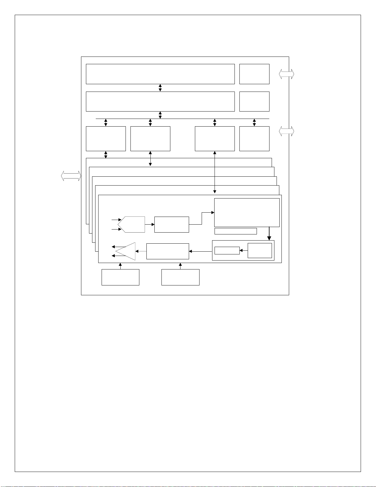
1.4 Block Diagram
Twisted
Pai r
Interface
10/100M
MAC
RXP4
RXN 4
TXP4
TXN4
A/D
CONV ERTER
DRIVER
Embedded Memory
Switching Fabric
10/100M
MAC
PORT 0
PORT 1
PORT2
...
PORT N
DIGITAL
EQUALIZER
MLT3 Converter
...
10/100M
MAC
PARTITION HANDLER
SCRAMBLER
LED
DISPLAY
CONTROL
Memory
BIST
10/100M
MAC
Data Handler
TRANSMIT
STATE
MACHINE
LED
Interface
MII
Interface
1.5 Abbreviations
BER Bit Error Rate
CFI Canonical Format Indicator
COL Collision
CRC Cyclic Redundancy Check
CRS Carrier Sense
CS Chip Select
DA Destination Address
DI Data Input
DO Data Output
EDI EEPROM Data Input
EDO EEPROM Data Output
EECS EEPROM Chip Select
CLOCK GENERATORBIAS
Figure 1-1 ADM6996F Block Diagram
ADMtek Inc. 1-3

ADM6996F Product Review
EESK EEPROM Clock
ESD End of Stream Delimiter
FEFI Far End Fault Indication
FET Field Effect Transistor
FLP Fast Link Pulse
GND Ground
GPSI General Purpose Serial Interface
IPG Inter-Packet Gap
LFSR Linear Feedback Shift Register
MAC Media Access Controller
MDIX MDI Crossover
MII Media Independent Interface
NRZI Non Return to Zero Inverter
NRZ Non Return to Zero
PCS Physical Coding Sub-layer
PHY Physical Layer
PLL Phase Lock Loop
PMA Physical Medium Attachment
PMD Physical Medium Dependent
QoS Quality of Service
QFP Quad Flat Package
RST Reset
RXCLK Receive Clock
RXD Receive Data
RXDV Receive Data Valid
RXER Receive Data Errors
RXN Receive Negative (Analog receive differential signal)
RXP Receive Positive (Analog receive differential signal)
SA Source Address
SOHO Small Office Home Office
SSD Start of Stream Delimiter
SQE Signal Quality Error
TOS Type of Service
TP Twisted Pair
TTL Transistor Transistor Logic
TXCLK Transmission Clock
TXD Transmission Data
TXEN Transmission Enable
TXN Transmission Negative
TXP Transmission Positive
ADMtek Inc. 1-4

ADM6996F Product Review
1.6 Conventions
1.6.1 Data Lengths
qword 64-bits
dword 32-bits
word 16-bits
byte 8 bits
nibble 4 bits
1.6.2 Pin Types
Pin Type Description
I Input
O Output
I/O Bi-directional
OD Open drain
SCHE Schmitt Trigger
PD internal pull-down
PU internal pull-up
1.6.2 Register Types
Register Type Description
RO Read-only
WO Write-only
RW Read/Write
ADMtek Inc. 1-5
ADM6996F Interface Description
Chapter 2 Interface Description
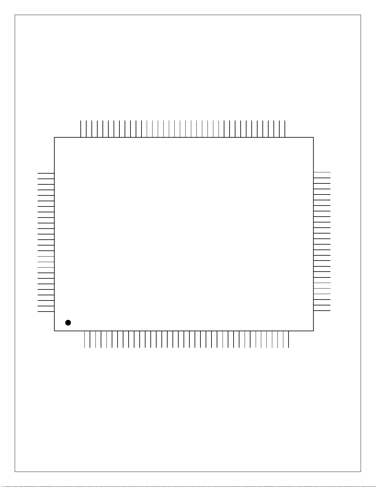
2.1 Pin Diagram
100
101
102
P4RXD3
P4RXD2
P4RXD1
99
LNKACT0
GNDO
97
98
LNKACT1
95
96
VCC2IK
LNKACT3
LNKACT2
72
73
74
75
76
77
78
79
80
81
82
83
84
85
86
87
88
89
90
91
92
93
94
P5RXCLK
P4RXDV
P4RXD0
VCC2IK
GNDIK
P4CRS
P4COL
EDI (DUAL COLOR)
EECS
EESK (XOVEN)
VCC2IK
GNDIK
EDO
CKO25M
CFG0
GNDO
VCC3O
SPDTNP5
LNKFP5
DPHALFP5
LNKFP4
GNDIK
70
71
GNDO
VCC3O
69
P5RXER
GNDO
68
P5TXCLK
676665
VCC2IK
P5TXEN(PHYAS0)
103
P4TXD3
104
P4TXD2
105
P4TXD1 (P4TYPE1)
106
P4TXD0 (P4TYPE0)
107
DPHALFP4
108
GNDO
109
VCC3O
110
DUPCOL3
111
DUPCOL2 (RECBPEN)
112
DUPCOL1(PHYAS1)
113
DUPCOL0(RECANEN)
114
P4TXEN
115
P4TXCLK
116
VCCIK
117
P4RXCLK
118
GNDIK
119
RC
120
XI
121
XO
122
VCCPLL
123
GNDPLL
124
CONTROL
125
VREF
126
GNDBIAS
127
RTX
128
VCCBIAS
VCCA2
TXP0
234
1
TXN0
GNDA
GNDA
5
RXN0
RXP0
678
ADM6996F
VCCAD
VCCA2
GNDA
TXN1
TXP1
101112131415161718192021222324252627282930
9
GNDA
RXP1
RXN1
VCCAD
VCCA2
TXN2
TXP2
GNDA
RXP2
RXN2
VCCAD
VCCA2
TXP3
TXN3
GNDA
GNDA
VCCAD
RXN4
RXN3
RXP3
31323334353637
RXP4
GNDA
GNDA
(GFCEN) P5TXD0
(P5GPSI) P5TXD1
P5TXD2
P5TXD3
P5COL
P5RXD3
P5RXD2
P5RXD1
P5RXD0
P5RXDV
SPDTNP4
GNDO
VCC3O
LDSPD3
LDSPD2
LDSPD1
LDSPD0
P4RXER
VCCA2
TXN4
TXP4
38
GNDIK
P4FX
P5CRS
VCCIK
GNDIK
MDC
TEST
MDIO
64
63
62
61
60
59
58
57
56
55
54
53
52
51
50
49
48
47
46
45
44
43
42
41
40
39
Figure 2-1 4 TP/FX PORT + 2 MII PORT 128 Pin Diagram
ADMtek Inc. 2-1
ADM6996F Interface Description
2.2 Pin Description by Function
ADM6996F pins are categorized into one of the following groups:
Section 2.2.1 Twisted Pair Interface
Section 2.2.2 5th Port (MII) Interfaces
Section 2.2.3 6th Port (MII) Interfaces
Section 2.2.4 LED Interface
Section 2.2.5 EEPROM/Management Interface
Section 2.2.6 Power/Ground, 48 pins
Section 2.2.7 Miscellaneous
Note:
“Section 1.6.2 Pin Types” can be used for reference.
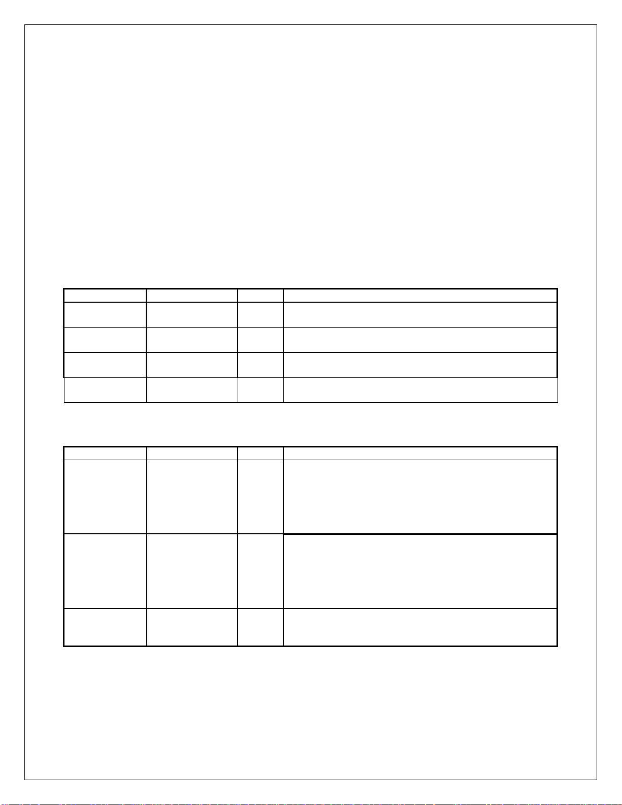
2.2.1 Twisted Pair Interface
Pin Name Pin# Type Descriptions
RXP[0:4] 6, 14, 21, 29, 33 I/O,
Analog
RXN[0:4] 7, 15, 22, 30, 32 I/O,
Analog
TXP[0:4] 2, 10, 18, 25, 37 I/O,
Analog
TXN[0:4] 3, 11, 19, 26, 36 I/O,
Analog
Twisted Pair Receive Input Positive.
Twisted Pair Receive Input Negative.
Twisted Pair Transmit Output Positive.
Twisted Pair Transmit Output Negative.
2.2.2 5th Port (MII) Interfaces
Pin Name Pin# Type Descriptions
P4TXD[0]
Setting
P4TYPE0
P4TXD[1]
Setting
P4TYPE1
P4TXD[3:2] 103, 104 I/O,
106 I/O,
8mA
PD
105 I/O,
8mA
PD
8mA
PD
Port4 MII transmit data 0
Acts as MII transmit data TXD[0]. Synchronous to the rising
edge of TXCLK.
Setting
P4TYPE0 : At power-on-reset, latched as P4 TYPE0.
Port4 MII Transmit Data bit 1
Synchronous to the rising edge of TXCLK. These pins act
as MII TXD[1].
Setting
P4TYPE1 : At power-on-reset, latched as P4 TYPE1.
Port4 MII Transmit Data bit 3~2
Synchronous to the rising edge of TXCLK. These pins act
as MII TXD[3:2].
ADMtek Inc. 2-2

ADM6996F Interface Description
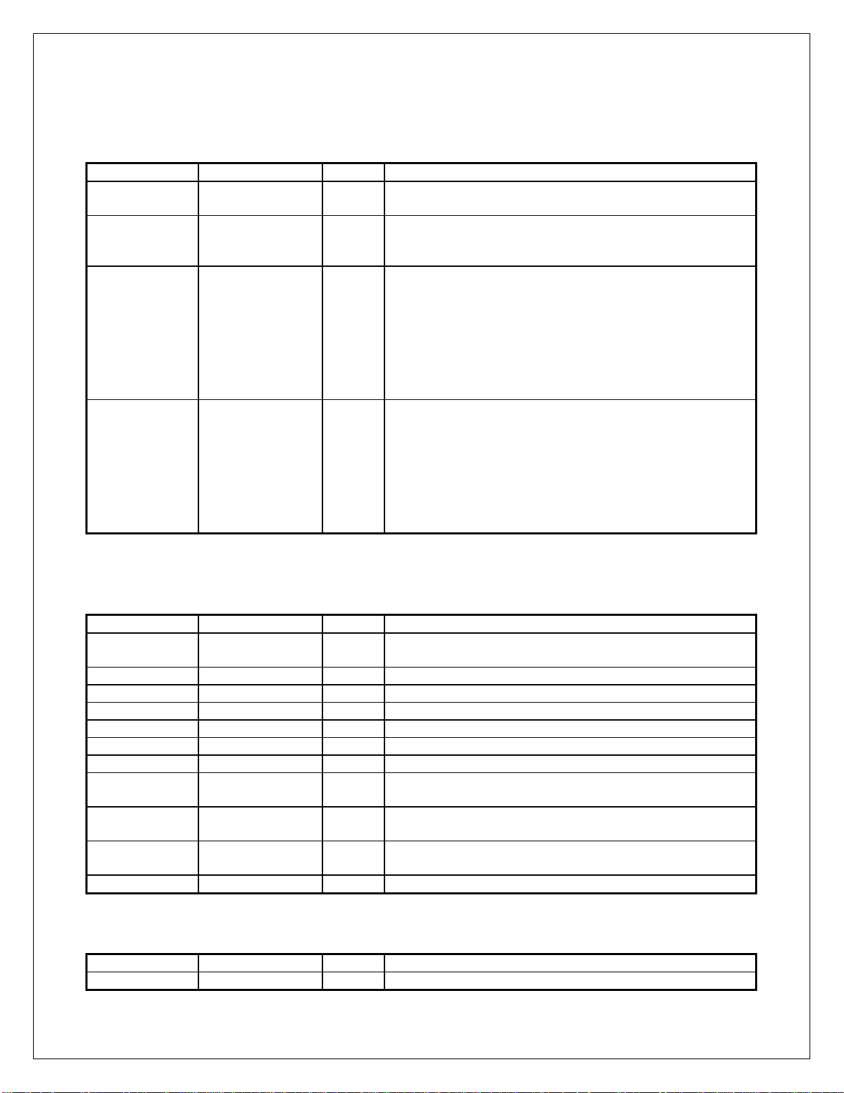
Pin Name Pin# Type Descriptions
P4FX 62 I
PD
Port4 FX/TX mode select. Internal pull down.
1: Port4 as FX port.
0: Port4 as TX port.
P4TXEN
P4RXD[0] 74 I
P4RXD[3:1] 102, 101,
P4RXDV 73 I
P4RXER 39 I
P4COL 78 I
P4CRS 77 I
P4RXCLK 117 I
P4TXCLK 115 I
DHALFP4 107 I
LNKFP4 92 I
SPDTNP4 51 I
114 I/O
8mA
PD
PD
100
PD
PD
PD
PD
PD
PD
PD
PD
PD
PD
Port4 MII Transmit Enable. Internal pull down.
Port4 MII port receive data 0
These pins act as MII RXD[0]. Synchronous to the rising
edge of P4RXCLK. Internal pull down.
I
Port4 MII port receive data 3~0
These pins act as MII RXD[3:0]. Synchronous to the rising
edge of P4RXCLK. Internal pull down.
Port4 MII receive data valid.
Internal pull down.
Port4 MII Port Receive Error.
Internal pull down.
Port4 MII Port Collision input
Internal pull down.
Port4 MII Port Carrier Sense
Internal pull down.
Port4 MII Port Receive Clock Input
Port4 MII Port Transmit clock Input
Port4 MII Port Hardware Duplex input pin.
Low: Full Duplex. High: Half Duplex.
Internal pull down.
Port4 MII Port Hardware Link input pin.
Low: Link OK. High: Link Off.
Internal pull down.
Port4 MII Port Hardware Speed input pin.
Low: 100M. High: 10M.
Internal pull down.
2.2.3 6th Port (MII) Interfaces
Pin Name Pin# Type Descriptions
P5TXD[0]
Setting
GFCEN
63 I/O,
8mA
PU
MII transmit data 0 /GPSI TXD
Acts as MII transmit data TXD[0]. Synchronous to the rising
edge of TXCLK.
Setting
GFCEN: Global Flow Control Enable.
At power-on-reset, latched as Full Duplex Flow control
setting
ADMtek Inc. 2-3

ADM6996F Interface Description
Pin Name Pin# Type Descriptions
“1” to enable flow-control (default ), “0” to disable flowcontrol.
P5TXD[1]
Setting
P5GPSI
P5TXD[3:2] 59, 60 I/O,
P5TXEN
Setting
PHYAS0
P5RXD[3:0] 56, 55, 54, 53 I
P5RXDV 52 I
P5RXER 68 I
P5COL 58 I
P5CRS 57 I
P5RXCLK 72 I
P5TXCLK 67 I
DHALFP5 91 I
61 I/O,
8mA
PD
8mA
PD
66 I/O
8mA
PD
PD
PD
PD
PD
PD
PD
PD
PD
MII Transmit Data bit 1
Synchronous to the rising edge of TXCLK. These pins act
as MII TXD[1].
Setting
P5GPSI: Port 5 GPSI Enable.
At power-on-reset, latched as P5 GPSI Enable.
“0” to disable port 5 GPSI (default ), “1” to enable port 5
GPSI.
Port5 MII Transmit Data bit 3~2
Synchronous to the rising edge of TXCLK. These pins act
as MII TXD[3:2].
Port5 MII Transmit Enable. Internal pull down.
Setting
PHYAS0: Chip physical address for multiple chip application
on read EEPROM data. Internal pull down.
Power on reset value PHYAS0 combines with PHYAS1
PHYAS1 PHYAS0
0 0 Master(93C46)
If there is no EEPROM then user must use 93C66 timing to
write chip’s register.
If user put 93C46 with correct Signature then user writes
chip register by 93C46 timing.
If user put 93C66 then data put in Bank0. User can write
chip register by 93C66 timing.
User must assert one SK cycle when CS at idle stage when
write chip internal register.
Port5 MII port receive data 3~0
These pins act as MII RXD[3:0]. Synchronous to the rising
edge of P5RXCLK. Internal pull down.
Port5 MII receive data valid.
Internal pull down.
Port5 MII Port Receive Error.
Internal pull down.
Port5 MII Port Collision input
Internal pull down.
Port5 MII Port Carrier Sense
Internal pull down.
Port5 MII Port Receive Clock Input
Port5 MII Port Transmit clock Input
Port5 MII Port Hardware Duplex input pin.
Low: Full Duplex. High: Half Duplex.
ADMtek Inc. 2-4

ADM6996F Interface Description
Pin Name Pin# Type Descriptions
Internal pull down.
LNKFP5 90 I
PD
SPDTNP5 89 I
PD
Port5 MII Port Hardware Link input pin.
Low: Link OK. High: Link Off.
Internal pull down.
Port5 MII Port Hardware Speed input pin.
Low: 100M. High: 10M.
Internal pull down.
2.2.4 LED Interface
Pin Name Pin# Type Descriptions
LNKACT[3:0] 95,
96, 97,
98
DUPCOL[3] 110 O,
DUPCOL[2]
Setting
BPEN
DUPCOL[1]
Setting
PHYAS1
DUPCOL[0]
Setting
ANEN
LDSPD[3:0] 48, 47, 43, 42 O,
111 O,
112 O,
113 O,
O,
8mA
8mA
8mA,
PU
8mA,
PD
8mA,
PU
8mA
LINK/Activity LED[3:0]. Active low
“1” indicates no link activity on cable
“0” indicates link okay on cable, but no activity and signals
on idle stage.
“Blinking” indicates link activity on cable.
Duplex/Collision LED[3]. Active low
“1” for half-duplex and “blinking” for collision indication
“0” for full-duplex indication
Duplex/Collision LED[2]. Active low
“1” for half-duplex and “blinking” for collision indication
“0” for full-duplex indication
Setting
BPEN: At power-on-reset, latched as Back Pressure setting
“1” to enable Back-Pressure (defaulted), “0” to disable Back
Pressure.
At power-on-reset, latched as Back Pressure setting “1” to
enable Back-Pressure (defaulted), “0” to disable Back
Pressure.
Duplex/Collision LED[1]. Active low
“1” for half-duplex and “blinking” for collision indication
“0” for full-duplex indication
Setting
PHYAS1: Power on Reset latch value combine with TXEN.
Internal pull down. Check pin 66.
Duplex/Collision LED[0]. Active low
“1” for half-duplex and “blinking” for collision indication
“0” for full-duplex indication
Setting
ANEN: On power-on-reset, latched as Auto Negotiation
capability for all ports.
“1” to enable Auto Negotiation ( defaulted by pulled up
internally ),
“0” to disable Auto Negotiation.
Speed LED[3:0]. Used to indicate corresponding port’s
speed status. “0” for 100Mb/s, “1” for 10Mb/s
ADMtek Inc. 2-5
ADM6996F Interface Description
2.2.5 EEPROM/Management Interface
Pin Name Pin# Type Descriptions
EDO 84 I,
TTL,PU
EECS 80 O,
4mA,PD
EECK
Setting
XOVEN
EDI
Setting
LEDMODE
81 I/O,
4mA
PD
79 I/O,
4mA
PD
EEPROM Data Output. Serial data input from EEPROM.
This pin is internally pull-up.
EEPROM Chip Select. This pin is active high chip enable
for EEPROM. When RESETL is low, it will be Tri-state.
Internally Pull-down
Serial Clock. This pin is clock source for EEPROM. When
RESETL is low, it will be tri-state.
Setting
XOVEN: This pin is internal pull-down. On power-on-reset,
latched as P4~0 Auto MDIX enable or not.
“0” to disable MDIX ( defaulted ), “1” to enable MDIX.
Suggest externally pull up to enable MDIX for all ports.
EEPROM Serial Data Input. This pin is output for serial
data transfer. When RESETL is low, it will be tri-state.
Setting
LEDMODE: This pin is internal pull-down. On power-onreset, latched as Dual Color mode or not.
“0” to set Single color mode for LED.
“1” to set Dual Color mode for LED.
2.2.6 Power/Ground, 48 pins
Pin Name Pin# Type Descriptions
GNDA 4,5,12, 13, 20, 27,
28, 34, 35
VCCA2 1, 9, 17, 24, 38 I 1.8V, Power Used by TX Line Driver.
VCCAD 8, 16, 23, 31 I 3.3V, Power Used by AD Block.
GNDBIAS 126 I Ground Used by Bias Block
VCCBIAS 128 I 3.3V, Power Used by Bias Block.
GNDPLL 123 I Ground used by PLL
VCCPLL 122 I 1.8V, Power used by PLL
GNDIK 45, 64, 76, 83, 93,
118
VCCIK 46, 65, 75, 82, 94,
116
GNDO 50, 69, 70, 87, 99,
108
VCC3O 49, 71, 88, 109 I 3.3V, Power Used by Digital Pad.
I Ground Used by AD Block.
I Ground Used by Digital Core
I 1.8V, Power Used by Digital Core
I Ground Used by Digital Pad
2.2.7 Miscellaneous
Pin Name Pin# Type Descriptions
CKO25M 85 O, 25M Clock Output.
ADMtek Inc. 2-6

ADM6996F Interface Description
Pin Name Pin# Type Descriptions
8mA
Control 124 O
RTX 127 Analog TX Resistor. Add 1.1K %1 resister to GND.
VREF 125 Analog Analog Reference Voltage.
RC 119 I,
SCHE
XI 120 I,
Analog
XO 121 O,
Analog
CFG0 86 I,
PU
MDIO 40 I/O,
8mA
PU
MDC 44 I,
SCHE
TEST 41 I,
PD
FET Control Signal.
The pin is used to control FET for 3.3V to 1.8V regulator.
RC Input for Power On reset. Reset input pin.
25M Crystal Input. 25M Crystal Input. Variation is limited to
+/- 50ppm.
25M Crystal Output. When connected to oscillator, this pin
should left unconnected.
Configuration of Port 4 MII Mode
CFG0 P4TYPE Description
0 00 5 Port and 1 MII interface
0 01 4 Port and 2 MII(MAC) interface
1 xx 4 Port and 1 MII(MAC) and 1 MII(PCS)
Management Data. MDIO transfers management data in
and out of the device synchronous to MDC.
Management Data Reference Clock. A non-continuous
clock input for management usage. ADM7001/T will use
this clock to sample data input on MDIO and drive data onto
MDIO according to rising edge of this clock.
TEST Value.
At normal application connect to GND.
ADMtek Inc. 2-7

ADM6996F Function Description
Chapter 3 Function Description
3.1 Functional Descriptions
The ADM6996F integrates four 100Base-X physical sub-layer (PHY), 100Base-TX
physical medium dependent (PMD) transceivers, four complete 10Base-T modules, 6
port 10/100 switch controller and two 10/100 MII/GPSI MAC and memory into a single
chip for both 10Mbits/s, 100Mbits/s Ethernet switch operation. It also supports 100BaseFX operation through external fiber-optic transceivers. The device is capable of operating
in either Full Duplex mode or Half-Duplex mode in 10Mbits/s and 100Mbits/s.
Operational modes can be selected by hardware configuration pins, software settings of
management registers, or determined by the on-chip auto negotiation logic.
The ADM6996F consists of three major blocks:
• 10/100M PHY Block
• Switch Controller Block
• Built-in SSRAM
The interfaces used for communication between PHY block and switch core is MII
interface.
Auto MDIX function is supported in this block. This function can be Enable/Disable by
hardware pin.
3.2 10/100M PHY Block
The 100Base-X section of the device implements the following functional blocks:
• 100Base-X physical coding sub-layer (PCS)
• 100Base-X physical medium attachment (PMA)
• Twisted-pair transceiver (PMD)
• The 100Base-X and 10Base-T sections share the following functional blocks.
• Clock synthesizer module
• MII Registers
• IEEE 802.3u auto negotiation
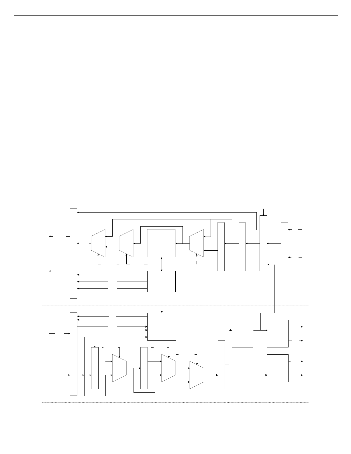
3.3 100Base-X Module
The ADM6996F implements 100Base-X compliant PCS and PMA and 100Base-TX
compliant TP-PMD as illustrated in Figure 2. Bypass options for each of the major
functional blocks within the 100Base-X PCS provides flexibility for various applications.
100Mbits/s PHY loop back is included for diagnostic purpose.
ADMtek Inc. 3-1
ADM6996F Function Description
3.4 100Base-X Receiver
The 100Base-X receiver consists of functional blocks required to recover and condition
the 125Mbits/s receive data stream. The ADM6996F implements the 100Base-X
receiving state machine diagram as given in ANSI/IEEE Standard 802.3u, Clause 24. The
125Mbits/s receive data stream may originate from the on-chip twisted-pair transceiver in
a 100Base-TX application. Alternatively, the receive data stream may be generated by an
external optical receiver as in a 100Base-FX application.
The receiver block consists of the following functional sub-blocks :
• A/D Converter
• Adaptive Equalizer and timing recovery module
• NRZI/NRZ and serial/parallel decoder
• De-scrambler
• Symbol alignment block
• Symbol Decoder
• Collision Detect Block
• Carrier sense Block
• Stream decoder block
CLOCK/DATA RECOVERY
SDP
10/100
TX
DRIVER
FIBER
OPTIC
DRIVER
RXP
RXN
ADAPTIVE EQUALIZER
TXP
TXN
FOTX+
FOTX-
RXD[1:0]
CRSDV
TXEN
TXD[1:0]
MII TO RMII CONVERTER
RMII TO MII CONVERTER
RXD[3:0]
BP_ALIGN
CRS
RXDV
RXER
COL
TXCLK
TXEN
TXER
TXD[3:0]
BP_4B5B
4B/5B DECODER
BP_4B5B
4B/5B
DECODER
RX STATE
MACHINE
TX STATE
MACHINE
BP_SCR
SCRAMBLER
BP_DSCR
100BASE-X RECEIVER
BP_ALIGN
DESCRAMBLER
SERIAL-TO-PARALLEL
MLT-3
STATE
MACHINE
PARALLAL-TO-SERIAL
100BASE-X TRANSMITTER
ADMtek Inc. 3-2
 Loading...