

ADMTK ADM6926 Datasheet

ADM6926
26 port 10/100 Mbps Ethernet Switch
Controller
Version 1.0
ADMtek.com.tw
Information in this document is provided in connection with ADMtek products. ADMtek may make
changes to specifications and product descriptions at any time, without notice. Designers must not rely on
the absence or characteristics of any features or instructions marked “reserved” or “undefined”. ADMtek
reserves these for future definition and shall have no responsibility whatsoever for conflicts or
incompatibilities arising from future changes to them
The products may contain design defects or errors know as errata, which may cause the product to deviate
from published specifications. Current characterized errata are available on request. To obtain latest
documentation please contact you local ADMtek sales office or visit ADMtek’s website at
http://www.ADMtek.com.tw
*Third-party brands and names are the property of their respective owners.

ADMtek Inc. V1.0
About this Manual
General Release
Intended Audience
ADMtek’s Customers
Structure
This Data sheet contains 5 chapters
Chapter 1 Product Overview
Chapter 2 Interface Description
Chapter 3 Function Description
Chapter 4. Electrical Specification
Chapter 5. Packaging
Revision History
Date Version Change
08 Aug 2003
1.0 1. First release of ADM6926
Customer Support
ADMtek Incorporated,
2F, No.2, Li-Hsin Rd.,
Science-based Industrial Park,
Hsinchu, 300, Taiwan, R.O.C.
Sales Information
Tel + 886-3-5788879
Fax + 886-3-5788871

ADMtek Inc. V1.0
Table of Contents
Chapter 1 Product Overview........................................................................................1-1
1.1 Overview.......................................................................................................... 1-1
1.2 Features............................................................................................................ 1-1
1.3 Block Diagram................................................................................................. 1-2
1.4 Abbreviations................................................................................................... 1-3
1.5 Conventions ..................................................................................................... 1-4
1.5.1 Data Lengths............................................................................................1-4
1.5.2 Register Type Descriptions......................................................................1-4
1.5.3 Pin Type Descriptions..............................................................................1-4
Chapter 2 Interface Description...................................................................................2-1
2.1 Pin Diagram – ADM6926 (SS-SMII Interface)..................................................... 2-1
2.2 Pin Description................................................................................................. 2-2
2.2.1 SS-SMII Networking Interface, 60 pins ...................................................2-2
2.2.2 MII/RMII Interface, 28pins......................................................................2-3
2.2.3 Power/Ground..........................................................................................2-5
2.2.4 Miscellaneous pins, 16 pins.....................................................................2-5
Chapter 3 Function Description...................................................................................3-1
3.1.1 Basic Operation.......................................................................................3-1
3.1.2 Address Learning.....................................................................................3-1
3.1.3 Address Aging..........................................................................................3-2
3.1.4 Address Recognition and Packet Forwarding.........................................3-3
3.1.5 Trunking Port Forwarding ......................................................................3-4
3.1.6 Illegal Frames..........................................................................................3-4
3.1.7 Back off Algorithm...................................................................................3-4
3.1.8 Buffers and Queues..................................................................................3-4
3.1.9 Half Duplex Flow Control.......................................................................3-5
3.1.10 Full Duplex Flow Control........................................................................3-5
3.1.11 Inter-Packet Gap (IPG) ...........................................................................3-5
3.1.13 Priority Control .......................................................................................3-6
3.1.14 Alert LED Display....................................................................................3-7
3.1.15 Broadcast Storm Filter ............................................................................3-7
3.1.16 Collision LED Display.............................................................................3-7
3.1.17 Bandwidth Control...................................................................................3-8
3.1.18 Smart Discard..........................................................................................3-8
3.1.19 Security Support.......................................................................................3-8
3.1.20 Smart Counter Support............................................................................3-8
3.1.21 Length 1536 Mode ...................................................................................3-8
3.1.22 PHY Management (MDC/MDIO Interface).............................................3-8
3.1.23 Forward Special Packets to the CPU Port..............................................3-9
3.1.24 Special TAG...........................................................................................3-10
3.1.25 Port 24 and Port 25 Interface (Only SS-SMII package support)...........3-12
3.1.26 Hardware, EEPROM and SMI Interface for Configuration..................3-13
3.2 EEPROM Register Format ............................................................................3-17
3.2.1 Signature (Index: 0h).............................................................................3-20
3.2.2 Global Configuration Register (Index: 1h)............................................3-20
ADM6926 i

ADMtek Inc. V1.0
3.2.3 Port Configuration Registers (Index: 2h ~ 1bh)....................................3-21
3.2.4 Miscellaneous Configuration (Index: 1ch)............................................3-23
3.2.5 VLAN(TOS) Priority Map (Index: 1dh).................................................3-23
3.2.6 Forwarding Group Outbound Port Map Low .......................................3-24
3.2.7 Forwarding Group Outbound Port Map High ......................................3-25
3.2.8 P0 VID and PVID Shift (Index: 5eh) .....................................................3-25
3.2.9 P1~P25 VID Configuration...................................................................3-26
3.2.10 P0, P1, P2, P3 Bandwidth Control Register (Index: 78h).....................3-26
3.2.11 P4, P5, P6, P7 Bandwidth Control Register (Index: 79h).....................3-27
3.2.12 P8, P9, P10, P11 Bandwidth Control Register (Index: 7ah).................3-27
3.2.13 P12, P13, P14, P15 Bandwidth Control Register (Index: 7bh).............3-28
3.2.14 P16, P17, P18, P19 Bandwidth Control Register (Index: 7ch).............3-28
3.2.15 P20, P21, P22, P23 Bandwidth Control Register (Index: 7dh).............3-29
3.2.16 P24, P25 Bandwidth Control Register (Index: 7eh)..............................3-29
3.2.17 Bandwidth Control Enable Register Low (Index: 7fh)..........................3-30
3.2.18 Bandwidth Control Enable Register High (Index: 80h)........................3-30
3.2.19 Reserved Registers (Index: 81h~8ah)....................................................3-30
3.2.20 Customized PHY Control Group 0 (Index: 8bh)....................................3-31
3.2.21 Customized PHY Control Group 1 (Index: 8ch)....................................3-31
3.2.22 Customized PHY Control Group 2 (Index: 8dh)....................................3-32
3.2.23 Customized PHY Control Group 3 (Index: 8eh)....................................3-32
3.2.24 Group 0 PHY Customized DATA 0 (Index: 8fh)....................................3-32
3.2.25 Group 0 PHY Customized DATA 1 (Index: 90h)...................................3-32
3.2.26 Group 1 PHY Customized DATA 0 (Index: 91h)...................................3-33
3.2.27 Group 1 PHY Customized DATA 1 (Index: 92h)...................................3-33
3.2.28 Group 2 PHY Customized DATA 0 (Index: 93h)...................................3-33
3.2.29 Group 2 PHY Customized DATA 1 (Index: 94h)...................................3-33
3.2.30 Group 3 PHY Customized DATA 0 (Index: 95h)...................................3-33
3.2.31 Group 3 PHY Customized DATA 1 (Index: 96h)...................................3-33
3.2.32 PHY Customized Enable Register (Index: 97h).....................................3-33
3.2.33 PPPOE Control Register0 (Index: 98h)................................................3-34
3.2.34 PPPOE Control Register 1 (Index: 99h)...............................................3-34
3.2.35 PHY Control Register 0 (Index: 9ah) ....................................................3-35
3.2.36 PHY Control Register 1 (Index: 9bh) ....................................................3-35
3.2.37 Disable MDIO Active Register 0 (Index: 9ch).......................................3-36
3.2.38 Disable MDIO Active Register 1 (Index: 9dh) ......................................3-36
3.2.39 Port Disable Register 0 (Index: 9eh).....................................................3-37
3.2.40 Port Disable Register 1 (Index: 9fh)......................................................3-37
3.2.41 IGMP Snooping Control Register 0 (Index: a0h)..................................3-37
3.2.42 IGMP Snooping Control Register 1 (Index: a1h)..................................3-38
3.2.43 CPU Control Register (Index: a2h).......................................................3-38
3.2.44 Special MAC Forward Control Register 0 (Index: a3h) .......................3-39
3.2.45 Special MAC Forward Control Register 2 (Index: a4h) .......................3-40
3.2.46 Special MAC Forward Control Register 2 (Index: a5h) .......................3-40
3.2.47 Trunking Enable Register 0 (Index: a6h) ..............................................3-41
3.2.48 Trunking Enable Register 1 (Index: a7h) ..............................................3-41
ADM6926 ii

ADMtek Inc. V1.0
3.3 Switch Register Map...................................................................................... 3-42
3.3.1 Version ID (Offset: 0h) ..........................................................................3-42
3.3.2 Link Status (Offset: 1h)..........................................................................3-42
3.3.3 Speed Status (Offset: 2h)........................................................................3-43
3.3.4 Duplex Status (Offset: 3h)......................................................................3-44
3.3.5 Flow Control Status (Offset: 4h)............................................................3-44
3.3.6 Address Table Control and Status Register...........................................3-45
3.3.7 PHY Control Register (Offset: bh).........................................................3-51
3.3.8 Hardware Status (Offset: dh).................................................................3-51
3.3.9 Receive Packet Count Overflow (Offset: eh).........................................3-52
3.3.10 Receive Packet Length Count Overflow (Offset: fh)..............................3-53
3.3.11 Transmit Packet Count Overflow (Offset: 10h).....................................3-53
3.3.12 Transmit Packet Length Count Overflow (Offset: 11h).........................3-54
3.3.13 Error Count Overflow (Offset: 12h)......................................................3-54
3.3.14 Collision Count Overflow (Offset: 13h).................................................3-55
3.3.15 Renew Counter Register (Offset: 14h)...................................................3-56
3.3.16 Read Counter Control & Status Register ..............................................3-57
3.3.17 Reload MDIO Register (Offset: 17h).....................................................3-57
3.3.18 Spanning Tree Port State 0 (Offset: 18h) ..............................................3-58
3.3.19 Spanning Tree Port State 1 (Offset: 19h) ..............................................3-58
3.3.20 Source Port Register (Offset: 1ah) ........................................................3-59
3.3.21 Transmit Port Register (Offset: 1bh).....................................................3-59
3.3.22 Counter Register: Offset Hex. 0100h ~ 019b.........................................3-59
Chapter 4 Electrical Specification................................................................................4-1
4.1 DC Characterization......................................................................................... 4-1
4.1.1 Absolute Maximum Rating.......................................................................4-1
4.1.2 Recommended Operating Conditions......................................................4-1
4.1.3 DC Electrical Characteristics for 3.3V Operation..................................4-1
4.2 AC Characterization......................................................................................... 4-2
4.2.1 XI/OSCI (Crystal/Oscillator) Timing.......................................................4-2
4.2.1 Power On Reset........................................................................................4-2
4.2.2 EEPROM Interface Timing......................................................................4-3
4.2.3 10Base-TX MII Output Timing ................................................................4-3
4.2.4 10Base-TX MII Input Timing...................................................................4-4
4.2.5 100Base-TX MII Output Timing ..............................................................4-5
4.2.6 100Base-TX MII Input Timing.................................................................4-5
4.2.7 Reduced MII Timing ................................................................................4-6
4.2.8 SS_SMII Transmit Timing........................................................................4-7
4.2.9 SS_SMII Receive Timing..........................................................................4-7
4.2.10 Serial Management Interface (MDC/MDIO) Timing..............................4-8
Chapter 5 Packaging......................................................................................................5-1
ADM6926 iii

ADMtek Inc. V1.0
List of Figures
Figure 1-1 ADM6926 Block Diagram............................................................................. 1-2
Figure 2-1 ADM6926 Pin Diagram ................................................................................. 2-1
Figure 3-1 The Search Pointer .......................................................................................3-48
Figure 3-2 Address Table Mapping to Output Port MAP.............................................. 3-50
Figure 4-1 Crystal/Oscillator Timing...............................................................................4-2
Figure 4-2 Power on reset timing.....................................................................................4-2
Figure 4-3 EEPROM Interface Timing............................................................................4-3
Figure 4-4 10Base-TX MII Output Timing ..................................................................... 4-3
Figure 4-5 10Base-TX MII Input Timing........................................................................ 4-4
Figure 4-6 100Base-TX MII Output Timing ................................................................... 4-5
Figure 4-7 100Base-TX MII Input Timing...................................................................... 4-5
Figure 4-8 Reduced MII Timing (1 of 2)......................................................................... 4-6
Figure 4-9 Reduced MII Timing (2 of 2)......................................................................... 4-6
Figure 4-10 SS_SMII Transmit Timing........................................................................... 4-7
Figure 4-11 SS_SMII Receive Timing ............................................................................ 4-7
Figure 4-12 Serial Management Interface (MDC/MDIO) Timing.................................. 4-8
List of Table
Table 4-4-1 Electrical Absolute Maximum Rating.......................................................... 4-1
Table 4-4-2 Recommended Operating Conditions .......................................................... 4-1
Table 4-4-3 DC Electrical Characteristics for 3.3V Operation........................................ 4-1
Table 4-4 Crystal/Oscillator Timing................................................................................ 4-2
Table 4-5 Power on reset timing...................................................................................... 4-3
Table 4-6 EEPROM Interface Timing............................................................................. 4-3
Table 4-7 10Base-TX MII Output Timing....................................................................... 4-4
Table 4-8 10Base-TX MII Input Timing ......................................................................... 4-4
Table 4-9 100Base-TX MII Output Timing..................................................................... 4-5
Table 4-10 100Base-TX MII Input Timing ..................................................................... 4-6
Table 4-11 Reduced MII Timing ..................................................................................... 4-6
Table 4-12 SS_SMII Transmit Timing............................................................................ 4-7
Table 4-13 SS_SMII Receive Timing.............................................................................. 4-8
Table 4-14 Serial Management Interface (MDC/MDIO) Timing ................................... 4-8
ADM6926 iv

ADM6926 Product Review
Chapter 1 Product Overview
1.1 Overview
The ADM6926 is a high performance/low cost, twenty six-port 10/100 Mbps Ethernet
Switch Controller with all ports supporting 10/100 Mbps full duplex switch function.
The ADM6926 is intended for applications to standalone-bridge for the low cost etherswitch market. ADM6926 can be programmed trunking port active. The trunking port
can be connected to server or stacking two switch boxes to enhance the performance.
The ADM6926 also supports back-pressure in half duplex mode and 802.3x flow control
in full duplex mode. When back-pressure is enabled, and there is no receive buffer
available for the incoming packet, the ADM6926 will force a JAM pattern on the
receiving port in half duplex mode and transmit the 802.3x packet back to receiving end
in full duplex mode.
An intelligent address recognition algorithm makes ADM6926 to recognize up to 4096
different MAC addresses and enables filtering and forwarding at full wire speed.
The ADM6926 has embedded SRAM for the proprietary buffer management. The SRAM
is used to store the incoming/outgoing packets. These buffers provide elastic storage for
transferring data between low-speed and high-speed segments and buffers are efficiently
allocated to improve the efficiency.
1.2 Features
• Support twenty four 10/100M auto-detect Half/Full duplex switch ports with SS-SMII
interface and two 10/100M Half/Full duplex port with RMII/MII interface
• Supports up to 4096 MAC addresses table (4-way hashing)
• Support two queue for QOS (1:2 or 1:4 or 1:8 or 1:16)
• Support Port-base, 802.1p and IP TOS priority
• Supports store & forward architecture and Performs forwarding and filtering at non-
blocking full wire speed
• Support buffer allocation with 256 bytes each
• Supports aging function and 802.3x flow control for full duplex and back-pressure
function for half duplex operation in case buffer is full
• Support packet length up to 1536 bytes
• Support Congestion Flow Control
• Broadcast storm filter and Alert LED
• Port-base VLAN and adjustable VLAN to support up to 32 VLAN group
• serial CPU interface for counter and port status output
• CPU can see-through to access PHY
• flexible port trunking on fault tolerance and load balance
• per port 32bits smart counter for Rx/Tx byte/packet count, error count and collision
count
ADMtek Inc. 1-1
ADM6926 Product Review
• rate-limit control (64K/128K/256K/512K/1M/4M/10M/20M)
• per port auto learning enable/disable and if disable, forward non-learned packet to
CPU
• MAC address table accessible (in each entry, reserve one bit for CPU to
enable/disable aging out)
• forward special multicast, BPDU, GMRP, GVRP and IGMP packets to CPU port
• 128 pin QFP package with 3.3V/1.8V power supply
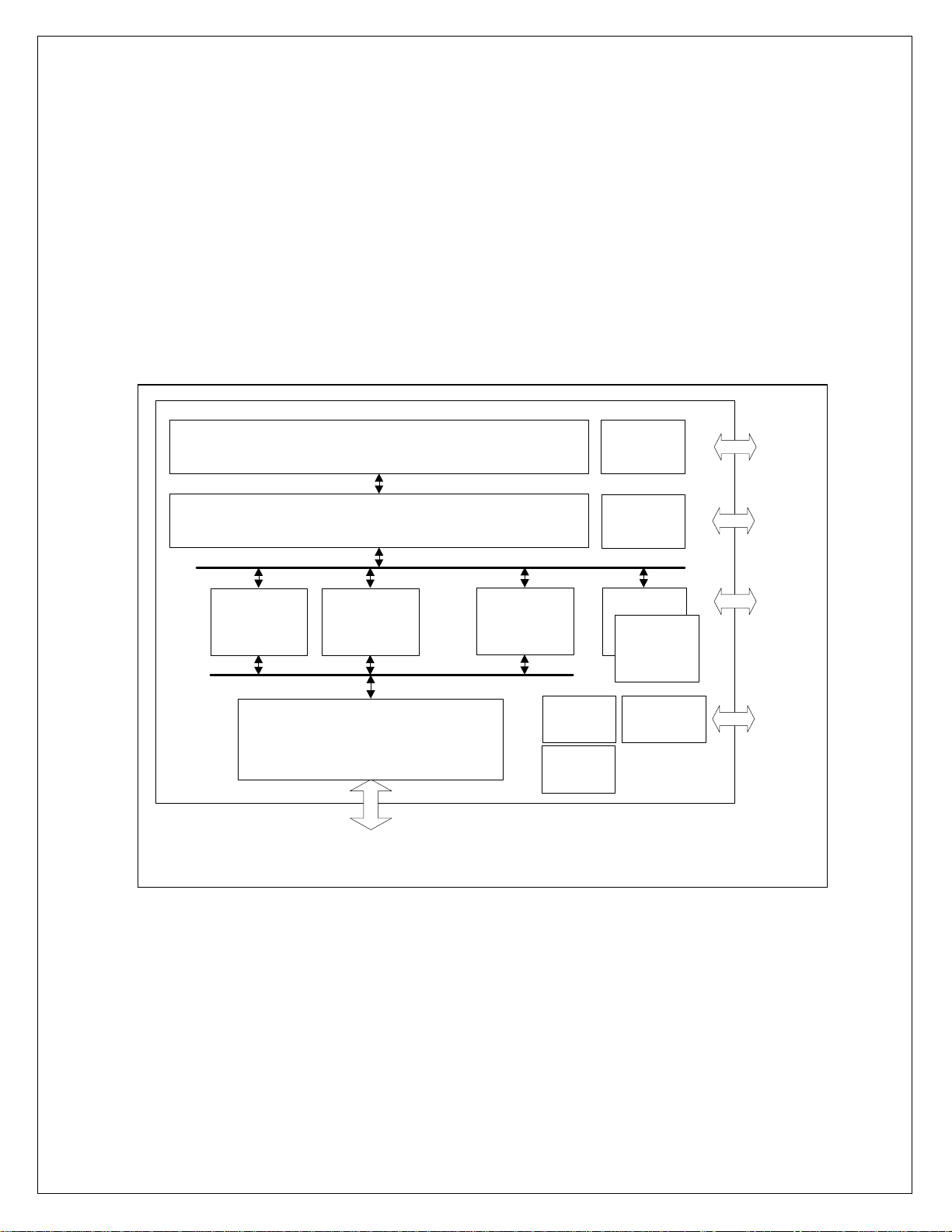
1.3 Block Diagram
10/100M
MAC
Embedded Memory
Switching Fa bric
10/100M
MAC
Interface Convertor
SS- SM I I
Interface
...
10/100M
MAC
CLOCK
GENERATOR
BIAS
Memory
BIST
EEPROM
Control
10/100M
10/100M
MAC
MAC
PHY Control
Cl ock /
LED
Interface
93C66
Interface
MII/RMII
Interface
MDC/
MDIO
Figure 1-1 ADM6926 Block Diagram
ADMtek Inc. 1-2

ADM6926 Product Review
1.4 Abbreviations
BPDU Bridge Protocol Data Unit
CRC Cyclic Redundancy Check
CRSDV Carrier Sense and Data Valid
DA Destination Address
DUPCOL Duplex and Collision
EDI EEPROM Data Input
EDO EEPROM Data Output
EECS EEPROM Chip Select
EESK EEPROM Serial Clock
ESD End of Stream Delimiter
FCS Frame Check Sequence
FET Field Effect Transistor
GARP Generic Attribute Registration Protocol
GMRP GARP Multicast Registration Protocol
GVRP GARP VLAN Registration Protocol
IGMP Internet Group Management Protocol
IPG Inter-Packet Gap
MAC Media Access Controller
MDC Management Data Clock
MDIO Management Data Input/Output
MII Media Independent Interface
PHY Physical Layer
PLL Phase Lock Loop
PPPoE Point to Point Protocol over Ethernet
PVID Port VLAN ID
QFP Quad Flat Pack
QOS Quality of Service
RMII Reduced Media Independent Interface
SA Source Address
SS-SMII Source Synchronous Serial MII
TA Turn Around
TOS Type of Service
TTL Transistor Transistor Logic
UNIQUE Universal Queue management
VID VLAN ID
VIH Voltage Input High
VIL Voltage Input Low
VLAN Virtual LAN
ADMtek Inc. 1-3

ADM6926 Product Review
1.5 Conventions
1.5.1 Data Lengths
qword 64-bits
dword 32-bits
word 16-bits
byte 8 bits
nibble 4 bits
1.5.2 Register Type Descriptions
Register Type Description
RO Read Only
R/W Read and Write capable
SC Self-clearing
LL Latching low, unlatch on read
LH Latching high, unlatch on read
COR Clear On Read
1.5.3 Pin Type Descriptions
Pin Type Description
I: Input
O: Output
I/O: Bi-directional
OD: Open drain
SCHE: Schmitt Trigger
PU: Pull Up
PD: Pull Down
ADMtek Inc. 1-4
ADM6926 Interface Description
Chapter 2 Interface Description
2.1 Pin Diagram – ADM6926 (SS-SMII Interface)
102
101
100
999897969594939291
M1TXCLK
M1RXCLK
M1RXDV
M1RXD[0]
M1RXD[1]
M1RXD[2]
M1RXD[3]
EESK
EDI
EDO
908988878685848382818079787776
M0RXD[1]
M0RXD[2]
M0RXD[3]
M1CRS
M1COL
M1TXD[3]
M1TXD[2]
M1TXD[1]
M1TXD[0]
VCCIK
GNDIK
M1TXEN
M0RXD[0]
VCC3O
GNDO
75
M0TXD[0]
M0TXEN
M0TXCLK
M0RXCLK
M0RXDV
M0TXD[2]
M0TXD[1]
7069686766
GNDIK
M0CRS
M0COL
M0TXD[3]
65
SRXD2[7]
VCCIK
71
72
73
74
103
104
105
106
107
108
109
110
111
112
113
114
115
116
117
118
119
120
121
122
123
124
125
126
127
128
ALERT
STXD0[0]
EECS
SRXD0[0]
STXD0[1]
SRXD0[1]
STXD0[2]
VCC3O
GNDO
SRXD0[2]
SYNC_TX0
STXD0[3]
SYNC_RX0
SRXD0[3]
CLK_TX0
STXD0[4]
CLK_RX0
SRXD0[4]
VCCIK
GNDIK
STXD0[5]
SRXD0[5]
STXD0[6]
SRXD0[6]
STXD0[7]
VCC3O
ADM6926
STXD2[7]
SRXD2[6]
STXD2[6]
SRXD2[5]
STXD2[5]
RESETL
SRXD2[4]
CLK_RX2
STXD2[4]
CLK_TX2
SRXD2[3]
SYNC_RX2
GNDO
VCC3O
GNDIK
VCCIK
STXD2[3]
SYNC_TX2
SRXD2[2]
STXD2[2]
SRXD2[1]
STXD2[1]
SRXD2[0]
STXD2[0]
SRXD1[7]
STXD1[7]
64
63
62
61
60
59
58
57
56
5
5
54
53
52
51
50
49
48
47
46
45
44
43
42
41
40
39
GNDO
SRXD0[7]
STXD1[0]
SRXD1[0]
CKO50M
STXD1[1]
CKO25M
SRXD1[1]
STXD1[2]
SRXD1[2]
VCCRG
GNDRG
VREF
CONTROL
VCCPLL
GNDPLL
SYNC_TX1
STXD1[3]
MDC
MDIO
TEST2XIXO
2
1
6453789
15
10
11
141316
12
171819
21
20
TEST1
SYNC_RX1
SRXD1[3]
CLK_TX1
VCC3O
GNDO
STXD1[4]
CLK_RX1
SRXD1[4]
STXD1[5]
VCCIK
GNDIK
SRXD1[5]
STXD1[6]
SRXD1[6]
34
33
32
24
23
22
2526272829
31
30
353637
38
Figure 2-1 ADM6926 Pin Diagram
ADMtek Inc. 2-1

ADM6926 Interface Description
2.2 Pin Description
ADM6926 pins are categorized into one of the following groups:
• Section 2.2.1 SS-SMII Networking Interface, 60 pins
• Section 2.2.2 MII/RMII Interface, 28pins
• Section 2.2.3 Power/Ground
• Section 2.2.4 Miscellaneous pins, 16 pins
2.2.1 SS-SMII Networking Interface, 60 pins
Name Type Pin # Description
SRXD0[0:7] I,
TTL
106,108,
112,116,
Port 0 to Port 7 SS-SMII Receive Data bit. The receive data
should be synchronous to the rising edge of CLK_RX0.
120,124,
126,2
SYNC_RX0 I,
TTL
115 Port 0 to Port 7 SS-SMII Synchronous signal. This signal is
synchronous to the rising edge of CLK_RX0. Active high
indicates the byte boundary.
CLK_RX0 I,
TTL
STXD0[0:7] O, TTL
8mA
119 Reference Receive Clock for Port 0 to Port 7. This signal is
125MHz input for SS-SMII interface.
104,107,
109,114,
Port 0 to Port 7 SS-SMII Transmit Data bit. The transmit
data is synchronous to the rising edge of CLK_TX0.
118,123,
125,127
SYNC_TX0 O, TTL
8mA
113 Port 0 to Port 7 SS-SMII Synchronous signal. This signal is
synchronous to the rising edge of CLK_TX0. Active high
indicates the byte boundary.
CLK_TX0 O, TTL
16mA
SRXD1[0:7] I,
TTL
117 Reference Transmit Clock for Port 0 to Port 7. This signal
is 125MHz output for SS-SMII interface.
4,8,10,26,
32,36,38,
Port 8 to Port 15 SS-SMII Receive Data bit. The receive
data should be synchronous to the rising edge of CLK_RX1.
40
SYNC_RX1 I,
TTL
25 Port 8 to Port 15 SS-SMII Synchronous signal. This signal
is synchronous to the rising edge of CLK_RX1. Active high
indicates the byte boundary.
CLK_RX1 I,
TTL
STXD1[0:7] O, TTL
8mA
31 Reference Receive Clock for Port 8 to Port 15. This signal
is 125MHz input for SS-SMII interface.
3,6,9,18,
30,33,37,
Port 8 to Port 15 SS-SMII Transmit Data bit. The transmit
data is synchronous to the rising edge of CLK_TX1.
39
SYNC_TX1 O, TTL
8mA
17 Port 8 to Port 15 SS-SMII Synchronous signal. This signal
is synchronous to the rising edge of CLK_TX1. Active high
indicates the byte boundary.
CLK_TX1 O, TTL 27 Reference Transmit Clock for Port 8 to Port 15. This
ADMtek Inc. 2-2

ADM6926 Interface Description
Name Type Pin # Description
16mA signal is 125MHz output for SS-SMII interface.
SRXD2[0:7] I,
TTL
42,44,46,
54,58,61,
Port 16 to Port 23 SS-SMII Receive Data bit. The receive
data should be synchronous to the rising edge of CLK_RX2.
63,65
SYNC_RX2 I,
TTL
53 Port 16 to Port 23 SS-SMII Synchronous signal. This
signal is synchronous to the rising edge of CLK_RX2. Active
high indicates the byte boundary.
CLK_RX2 I,
TTL
STXD2[0:7] O, TTL
8mA
57 Reference Receive Clock for Port 16 to Port 23. This signal
is 125MHz input for SS-SMII interface.
41,43,45,
48,56,60,
Port 16 to Port 23 SS-SMII Transmit Data bit. The
transmit data is synchronous to the rising edge of CLK_TX2.
62,64
SYNC_TX2 O, TTL
8mA
47 Port 16 to Port 23 SS-SMII Synchronous signal. This
signal is synchronous to the rising edge of CLK_TX2. Active
high indicates the byte boundary.
CLK_TX2 O, TTL
16mA
55 Reference Transmit Clock for Port 16 to Port 23. This
signal is 125MHz output for SS-SMII interface.
2.2.2 MII/RMII Interface, 28pins
Name Type Pin # Description
M0CRS I,
TTL
68
MII Port0 Carrier Sense
This pin is internal pull_down.
PD
M0COL I,
TTL
69
MII Port0 Collision input
This pin is internal pull_down.
PD
M0TXD
[0:3]
I/O,
TTL
8mA
PD
73,72,71,
70
MII Port 0 Transmit Data Bit[0:3].
Synchronous to the rising edge of M0TXCLK.
RMII Port 0 Transmit Data Bit[0:1].
Synchronous to the rising edge of M0RXCLK.
RMIIMODE[1] : Value on M0TXD[3] will be latched at the
rising edge of RESETL to configure port 25 as RMII mode.
RMIIMODE[0] : Value on M0TXD[2] will be latched at the
rising edge of RESETL to configure port 24 as RMII mode.
M0TXEN I/O,
TTL
8mA
74
MII/RMII Port 0 Transmit Enable.
AGDIS. Value on this pin will be latched at the rising edge
of RESETL to set aging disable.
PD
M0TXCLK I,
TTL
75
MII Port 0 Transmit clock Input.
This pin is 25MHz input for MII interface.
PD
M0RXCLK I,
TTL
PD
76
MII/RMII Port 0 Receive Clock Input.
This pin is 25MHz input for MII interface and 50MHz
REFCLK input for RMII interface.
ADMtek Inc. 2-3

ADM6926 Interface Description
Name Type Pin # Description
M0RXDV I,
TTL
PD
M0RXD
[0:3]
I,
TTL
PD
77
80,81,82,
83
MII Port 0 Receive Data Valid.
RMII Port 0 Carrier Sense/Receive Data Valid.
This pin is internal pull_down.
MII Port 0 Receive Data Bit[0:3].
RMII Port 0 Receive Data Bit[0:1].
If in RMII mode, M0RXD[3] used for ext_dup_enable and
M0RXD[2] used for ext_dup_full. Internal pull_down. See
Sec3.1.27 for details.
M1CRS I,
TTL
84
MII Port 1 Carrier Sense
This pin is internal pull_down.
PD
M1COL I,
TTL
85
MII Port 1 Collision input
This pin is internal pull_down.
PD
M1TXD
[0:3]
I/O,
TTL
8mA
89,88,87,
86
MII Port 1Transmit Data Bit[0:3].
Synchronous to the rising edge of M1TXCLK.
RMII Port 1Transmit Data Bit[0:1].
Synchronous to the rising edge of M1RXCLK.
BPEN. Value on M1TXD[3] will be latched at the rising
edge of RESETL to set Back_pressure enable. Internal
pull_up.
FCEN. Value on M1TXD[2] will be latched at the rising
edge of RESETL to set flow control enable. Internal pull_up.
TNKEN. Value on M1TXD[1] will be latched at the rising
edge of RESETL to set trunking enable. Internal pull_up.
IPGLVING. Value on M1TXD[0] will be latched at the
rising edge of RESETL to set shorter IPG. Internal
pull_down.
M1TXEN O, TTL
8mA
PU
M1TXCLK I,
TTL
92
MII Port 1 Transmit Enable.
ANEN. Value on this pin will be latched at the rising edge of
RESETL to set auto_negotiation enable. Internal pull_up.
93 MII Port1 Transmit clock Input. This signal is 25MHz
input for MII interface.
PD
M1RXCLK I,
TTL
94 MII1 Receive Clock Input. This signal is 25MHz input for
MII interface and 50MHz REFCLK input for RMII interface.
PD
M1RXDV I,
TTL
95
MII/RMII Port 1 Receive Data Valid.
This pin is internal pull_down.
PD
M1RXD
[0:3]
I,
TTL
PD
96,97,98,
99
MII Port 1 Receive Data Bit[0:3].
RMII Port 1 Receive Data Bit[0:1].
If in RMII mode, M1RXD[3] used for ext_dup_enable and
M1RXD[2] used for ext_dup_full. Internal pull_down. See
Sec3.1.27 for details.
ADMtek Inc. 2-4

ADM6926 Interface Description
p
2.2.3 Power/Ground
Pin Name Pin Type Pin # Pin Description
GNDRG Analog
12 Ground for Regulator
Ground
VCCRG Analog
11 3.3V Power supply for Regulator
Power
GNDPLL Analog
16 Ground for PLL
Ground
VCCPLL Analog
15 1.8V Power supply PLL
Power
GNDIK Digital
Ground
VCCIK Digital
Power
GNDO Digital
Ground
VCC3O Digital
Power
35,50,67,
91,122
34,49,66,
90,121
1,29,52,
79,111
28,51,78,
110,128
Ground for Core Logic
1.8V Power supply for Core Logic
Ground for I/O PAD
3.3V Power supply for I/O PAD
2.2.4 Miscellaneous pins, 16 pins
Pin Name Pin Type Pin # Pin Description
CK25MO O, TTL
7 25MHz clock Output. This pin will drive out 25Mhz.
16mA
CK50MO/
COL_LED_
10M
XI I,
XO O,
O, TTL
16mA
Analog
5 50MHz clock Output. This pin will drive out 50MHz.
COL_LED_10M. This pin shows collision LED for 10M
domain (see EEPROM Register 1ch, Bit[9])
22 Crystal or OSC 50MHz Input. This is the clock source of
PLL. The PLL will generate 125Mhz for SS-SMII and
50MHz for RMII and 25Mhz for MII.
23
Crystal 50Mhz Output.
Analog
RESETL I, TTL
SCHE
ALERT/
COL_LED_
O, TTL
8mA
100M
59 Reset Signal. An active low signal with minimum 100ms
duration is required.
103 Alert LED Display. This pin will show the status of power-
on-diagnostic and broadcast traffic.
COL_LED_100M. This pin shows collision LED for 100M
domain (see EEPROM Register 1ch, Bit[9])
TEST[2:1] I,
TTL
21,24
Industrial Test pins.
These pins are internal pull_down.
PD
MDC O, TTL
16mA
19
Management Data Clock.
This pin output 2.2MHz clock to drive PHY and access
corres
onding speed and duplex and link status through
ADMtek Inc. 2-5

ADM6926 Interface Description
Pin Name Pin Type Pin # Pin Description
MDIO.
MDIO I/O,
20
TTL
8mA
PU
EESK I/O,
100
TTL
4mA
PU
EECS I/O,
105 EEPROM Chip Select. This pin is chip enable for EEPROM.
TTL
4mA
PD
EDI I/O,
101
TTL
4mA
PU
EDO I,
102
TTL
PU
CONTROL O,
14
Analog
VREF I,
13
Analog
Management Data.
This pin is in-out to PHY. When RESETL is low, this pin will
be tri-state. This pin is internal pull_up.
EEPROM Serial Clock.
This pin is clock source for EEPROM. When RESETL is low,
it will be tri-state. This pin is internal pull-up.
When RESETL is low, it will be tri-state. This pin is internal
pull-down.
EEPROM Serial Data Input.
This pin is output for serial data transfer. When RESETL is
low, it will be tri-state. This pin is internal pull-up.
EEPROM Serial Data Output.
This pin is input for serial data transfer. This pin is internal
pull-up.
FET Control Signal.
The pin is used to control FET for 3.3V to 1.8V regulator.
Regulator Control Input Signal.
ADMtek Inc. 2-6

ADM6926 Function Description
Chapter 3 Function Description
3.1 Introduction
The ADM6926 uses a “store & forward” switching approach for the following reasons:
1) Store & forward switches allow switching between different speed media (e.g.
10BaseX and 100BaseX). Such switches require the large elastic buffers, especially
bridging between a server on a 100Mbps network and clients on a 10Mbps segment.
2) Store & forward switches improve overall network performance by acting as a
“network cache”
3) Store & forward switches prevent the forwarding of corrupted packets by the frame
check sequence (FCS) before forwarding to the destination port.
3.1.1 Basic Operation
The ADM6926 receives incoming packets from one of its ports, uses the source address
(SA) and VID to update the address table, and then forwards the packet to the output
ports determined by the destination address (DA) and VID.
If the DA and VID are not found in the address table, the ADM6926 treats the packet as a
broadcast packet and forwards the packet to the other ports within the same group.
The ADM6926 automatically learns the port number of attached network devices by
examining the SA and VID of all incoming packets. If the SA and VID are not found in
the address table, the device adds it to the table.
3.1.2 Address Learning
The ADM6926 provides two ways to create the entry in the address table: dynamic
learning and manual learning. A four-way hash algorithm is implemented to allow 4
different addresses to be stored at the same location. Up to 4k entries can be created and
all entries are stored in the internal SSRAM. Two parameters, SA and VID, are combined
to generate the 10-bit hash key to allow that the same addresses with different port
number can exist in the table at the same time.
1. Dynamic Learning
The ADM6926 searches for SA and VID of an incoming packet in the address table and
acts as follows:
If the SA+VID was not found in the address table (a new address), the ADM6926 waits
until the end of the packet (non-error packet) and updates the address table. If the
ADMtek Inc. 3-1

ADM6926 Function Description
SA+VID was found in the address table, then aging value of each corresponding entry
will be reset to 0.
Dynamic learning will be disabled in the following condition:
(1) Security violation happened.
(2) The packet is a PAUSE frame.
(3) The first bit of SA is 1’b1.
(4) The packet is an error packet (too long, too short or FCS error).
(5) The CPU port leaning function is disabled or enabled but the CPU port instructs
the switch not to learn the packet.
(6) The port is in the Disabled or Blocking-not-Listening state in the Spanning Tree
Protocol.
2. Manual Learning
The ADM6926 implements the manual learning through the CPU’s help. The CPU can
create or remove any entry in the address table. Each entry could be static or pointed to
the output port map table. “Static” means the entry will not be aged forever. It is useful in
the security function (forward unknown packets to the CPU port or discard) or monitor
function (forward monitored address to the specific port). Output port map table is also
helpful in the IGMP function (if the number of the output port is more than one) or the
users want to redirect the special packets with reserved DA.
3.1.3 Address Aging
The ADM6926 will periodically (300ms) remove the non-static address in the address
table. This could help to prevent a station leaves the network and occupies a table space
for a long time. Aging function can be disabled from the hardware pin.
ADMtek Inc. 3-2

ADM6926 Function Description
b
p
p
p
3.1.4 Address Recognition and Packet Forwarding
The ADM6926 forwards the incoming packets between bridge ports according to the DA
and VID as follows:
DA
Unicast Address
Broadcast Address
(All 1’b1)
DA+VID was found in the
address table (entry not pointed
to the output port map table)
Forward packets to the port
determined by the address table.
The packet may be dropped
ecause of forwarding group
boundary violation.
Drop or forward to CPU Drop or forward to CPU Drop or forward to CPU
Forwarding packets to the other
ports within the same
forwarding group.
Drop or forward to CPU Drop or forward to CPU Drop or forward to CPU
DA+VID was found in the
address table (entry pointed to the
output port map table)
No Security Violation
Forward packets to the ports
determined by the output port
map table constrained by the
forwarding group.
Security Violation
No Security Violation
Forward packets to the ports
determined by the output port
map table constrained by the
forwarding group.
Security Violation
No Security Violation
DA+VID was not found in the
address table
Forward packets to the other
orts within the same forwarding
group.
Forward packets to the other
orts within the same forwarding
group.
Reserved Address
(01-80-c2-00-00-xx,
with the option to
forward normally)
Reserved Address
(01-80-c2-00-00-xx,
with the option to
forward to CPU)
Reserved Address
(01-80-c2-00-00-xx,
with the option to
discard)
IGMP Packet
(Port Enable IGMP)
Forwarding packets to the other
ports within the same
forwarding group.
Same as the above Same as the above Same as the above
Forward the packet to the CPU
port.
Same as the above Same as the above Same as the above
Discard the packet. Discard the packet. Discard the packet.
Same as the above Same as the above Same as the above
Forward the packet to the CPU
port.
Forward packets to the ports
determined by the output port
map table constrained by the
forwarding group.
Security Violation
No Security Violation
Forward the packet to the CPU
port.
Security Violation
No Security Violation
Security Violation
No Security Violation
Forward the packet to the CPU
port.
Security Violation
Forward packets to the other
orts within the same forwarding
group.
Forward the packet to the CPU
port.
Forward the packet to the CPU
port.
Drop or forward to CPU Drop or forward to CPU Drop or forward to CPU
ADMtek Inc. 3-3

ADM6926 Function Description
b
p
b
DA
IGMP Packet
(Port Disable IGMP)
Others
DA+VID was found in the
address table (entry not pointed
to the output port map table)
Forward packets to the port
determined by the address table.
The packet may be dropped
ecause of forwarding group
boundary violation.
Drop or forward to CPU Drop or forward to CPU Drop or forward to CPU
Forward packets to the port
determined by the address table.
The packet may be drop
ecause of forwarding group
boundary violation.
Drop or forward to CPU Drop or forward to CPU Drop or forward to CPU
DA+VID was found in the
address table (entry pointed to the
output port map table)
No Security Violation
Forward packets to the ports
determined by the output port
map table constrained by the
forwarding group.
Security Violation
No Security Violation
Forward packets to the ports
determined by the output port
ed
map table constrained by the
forwarding group.
Security Violation
DA+VID was not found in the
address table
Forward packets according the
Multicast Option.
Forward packets according the
Multicast Option.
3.1.5 Trunking Port Forwarding
ADM6926 supports the trunking forwarding and any port could be assigned to the
trunking port. When one or more of the members link fail, the ADM6926 will
automatically change the transmit path from the failed link port to normal link port. Port
based load balancing is implemented to distribute the loading.
3.1.6 Illegal Frames
The ADM6926 will discard all illegal frames such as runt packet (less than 64 bytes),
oversize packet (greater than 1518 or 1522 bytes) or bad CRC.
3.1.7 Back off Algorithm
The ADM6926 implements the truncated exponential back off algorithm compliant to the
802.3 standard. ADM6926 will restart the back off algorithm by choosing 0-9 collision
count. After 16 consecutive retransmit trials, the ADM6926 resets the collision counter.
3.1.8 Buffers and Queues
The ADM6926 incorporates 26 transmit queues and receive buffer area for the 26
Ethernet ports. The receive buffers as well as the transmit queues are located within the
ADM6926 along with the switch fabric. The buffers are divided into 640 blocks of 256
ADMtek Inc. 3-4

ADM6926 Function Description
bytes each. The queues of each port are managed according to each port’s read/write
pointer.
Input buffers and output queues are maintained through proprietary patent pending
UNIQUE (Universal Queue management) scheme.
3.1.9 Half Duplex Flow Control
Back-pressure is supported for half-duplex operation.
When the ADM6926 cannot allocate a receive buffer for an incoming packet (buffer full),
the device will transmit a jam pattern on the port, thus forcing a collision.
3.1.10 Full Duplex Flow Control
When full duplex port runs out of its receive buffer, a PAUSE command will be issued
by ADM6926 to notice the packet sender to pause transmission. This frame based flow
control is totally compliant to IEEE 802.3x. When flow control hardware pin is set to
high during power on reset and per port PAUSE is enabled, ADM6926 will output and
accept 802.3x flow control packet.
3.1.11 Inter-Packet Gap (IPG)
IPG is the idle time between any two successive packets from the same port. The value is
9.6us for 10Mbps ETHERNET and 960ns for 100Mbps fast Ethernet.
3.1.12 Port VLAN or Tag VLAN Support
Two VLAN settings are supported by the ADM6926: the port-based VALN or the tag-
based VLAN. For the port-based VLAN the ADM6926 will use the port number as the
index to lookup the forwarding table. For the tag-based VLAN, the ADM6926 will use
the VID to lookup the forwarding table. Each port is assigned a Port VID as the Default
VID if tag-based VLAN is used. The ADM6926 will check TAG, remove TAG, insert
TAG, and re-calculate CRC if packet is changed:
ADMtek Inc. 3-5
ADM6926 Function Description
(1) Packets received are untagged
Force no
tag
Don’t Care
Bypass
No No Untag as the original.
Yes No Untag as the original
No Yes Add Tag.
Yes Yes Untag as the original
Output port
is tagged or
not
(2) Packets received are tagged
Force no
tag
No No No The Tag is removed.
Yes No No
No Yes No
No No Yes
No Yes Yes
Yes Yes No
Yes No Yes
Yes Yes Yes
Bypass
Output port
is tagged or
not
Tag as the original. The priority in the TAG header is not checked and VID will not
change even if VID is 0 or 1.
Tag as the original. The priority in the TAG header is checked and if the VID is 0 or
1, it may change to PVID (see EEPROM register 1ch, Bit[3])
Tag as the original. The priority in the TAG header is checked and if the VID is 0 or
1, it may change to PVID (see EEPROM register 1ch, Bit[3])
Tag as the original. The priority in the TAG header is checked and if the VID is 0 or
1, it may change to PVID (see EEPROM register 1ch, Bit[3])
Tag as the original. The priority in the TAG header is not checked. The VID will not
change.
The Tag will be added and packet will be double tagged output. The VID will not
change.
Tag as the original. The priority in the TAG header is not checked. The VID will not
change.
3.1.13 Priority Control
Action
Action
The ADM6926 provides two priority queues on each output port. Five ways could be
used to assign a priority to a packet.
(1) The priority assigned to each receiving port.
(2) The priority field in the 802.1Q Tag Header.
(3) The IPv4 TOS field in the IPv4 Header.
(4) Priority assigned by the CPU.
(5) Management packet (high priority assigned).
ADMtek Inc. 3-6
ADM6926 Function Description
3.1.14 Alert LED Display
Two functions are displayed through the Alert LED.
1. Diagnostic mode after power on.
a) After reset or power up, LED keeps on at least 3 second, and processes internal
SSRAM self-test.
b) If test passes, the ADM6926 turns off LED and goes to the broadcast storm mode.
c) If SSRAM test fails, the ADM6926 turns off LED, then keeps on.
2. Broadcast storm mode after SSRAM self-test. Packets with DA = 48’hffffffffffff
will be counted into the storm counter.
Two thresholds (rising and falling) are used to control the broadcast storm.
a) Time Scale: 50ms is used. The max packet number in 100BaseT is 7490. The max
packet number in 10BaseT is 749.
b) Port Rising Threshold.
Broadcast Storm
Threshold.
All 100TX Disable 10% 20% 40%
Not All 100TX Disable 1% 2% 4%
00 01 10 11
c) Port Falling Threshold
Broadcast Storm
Threshold.
All 100TX Disable 5% 10% 20%
Not All 100TX Disable 0.5% 1% 2%
00 01 10 11
3.1.15 Broadcast Storm Filter
If broadcast storming filter is enabled, the broadcast packets (DA = 48’hffff-ffff-ffff)
over the rising threshold within 50 ms will be discarded when the alert LED is turned on.
3.1.16 Collision LED Display
Two collision LEDs are supported. (see EEPROM Register 1ch, Bit[9])
1) 100M Collision LED. If collision happens in one of the ports configured 100M,
the 100M Collision LED will flash in rate of 2Hz.
2) 10M Collision LED. If collision happens in one of the ports configured 10M, the
10M Collision LED will flash in rate of 2Hz.
ADMtek Inc. 3-7
ADM6926 Function Description
3.1.17 Bandwidth Control
The ADM6926 allows the user to limit the bandwidth for each input or output port. 64k,
128K, 256k, 512K, 1M, 4M, 10M and 20M are supported.
3.1.18 Smart Discard
The ADM6926 supports a smart mechanism to discard packets early according to their
priority to prevent the resource blocked by the low priority. The discard ratio is as follows:
Discard Mode
Utilization
00 0% 0% 0% 0%
01 0% 0% 25% 50%
11 0% 25% 50% 75%
00 01 10 11
3.1.19 Security Support
4 level security schemes are supported by the ADM6926. All the security violation
address will not be automatically learned.
The violated packet could be forwarded to the CPU port for management or discarded.
When CPU is not present, ADM6926 also provides a simple way to lock the first address
to prevent illegal address access.
3.1.20 Smart Counter Support
Six counters per port are supported by the ADM6926.
1) Receive Packet Count.
2) Receive Packet Length Count.
3) Transmit Packet Count.
4) Transmit Packet Length Count.
5) The Error Count
6) The Collision Count.
3.1.21 Length 1536 Mode
The ADM6926 provides a function to enable the port to receive packets up to 1536 Byte.
3.1.22 PHY Management (MDC/MDIO Interface)
The ADM6926 uses the MDC/MDIO interface to set the PHY status. After the reset or
power up, the MDC/MDIO controller will delay about 130ms to wait for the PHY to
ready. The ADM6926 supports two ways to configure the PHY setting.
1) PHY master. The switch only reads the PHY status (speed, duplex, link, and
pause). This mode is useful when users want to configure PHY through the CPU
help. The ADM6926 supports an indirect way (a PHY Control Register) for CPU
to access PHYs.
2) PHY slave. The switch uses the EEPROM setting to control the PHY attached
(only speed, duplex, link, and pause are supported). After the port setting
changed, the ADM6926 will use the new setting to program the PHY again and
update the status. 8 commands are provided in this mode to allow the customer to
customize the PHY setting.
ADMtek Inc. 3-8

ADM6926 Function Description
Note:
The PHY address attached to port 0 is 5’h8, the PHY address attached to port 1 is 5’h9,..,
the PHY address attached to port 23 is 5’h1f, the PHY address attached to port 24 is 5’h7
and the PHY address attached to port 25 is 5’h8.
3.1.23 Forward Special Packets to the CPU Port (IGMP and Spanning Tree Support)
ADM6926 will forward the special packets to the CPU port to provide the management
function.
1) DA is 01-80-C2-00-00-00 (BPDU)
2) DA is 01-80-C2-00-00-02 (Slow Protocol)
3) DA is 01-80-C2-00-00-03 (802.1x PAE)
4) DA is 01-80-C2-00-00-04 ~ 01-80-C2-00-00-0f
5) DA is 01-80-C2-00-00-20 (GMRP)
6) DA is 01-80-C2-00-00-21 (GVRP)
7) DA is 01-80-C2-00-00-22 (GVRP)
8) DA is 01-00-5E-xx-xx-xx and protocol field is 2 for IPV4 (IGMP)
ADMtek Inc. 3-9
ADM6926 Function Description
3.1.24 Special TAG
The ADM6926 has an ability to insert 4Byte special TAG when packets transmitted to
the CPU port or to remove 8Byte additional TAG in the packets when packets are
received from the CPU port. The configuration is shown in the CPU Configuration
Register. This special function allows the CPU to know the source port which will be
used in the IGMP Snooping , Spanning Tree or the Security function. The CPU also
could insert additional 8-byte Tag to instruct the switch to handle the packets. The
packets format is as follows:
Transmit End
7 OCTETS
1 OCTET
6 OCTETS
6 OCTETS
4 OCTETS
2 OCTETS
46--1500
OCTETS
4 OCTETS
Receive End
7 OCTETS
1 OCTET
6 OCTETS
6 OCTETS
8 OCTETS
2 OCTETS
46--1500
OCTETS
4 OCTETS
PREAMBLE
SFD
SFD
DESTINATION ADDRESS
SOURCE ADDRESS
Special TAG
LENGTH/TYPE
MAC CLIENT DATA
MAC CLIENT DATA
PAD
FRAME CHECK SEQUENCE
PREAMBLE
SFD
SFD
DESTINATION ADDRESS
SOURCE ADDRESS
Special TAG
LENGTH/TYPE
MAC CLIENT DATA
MAC CLIENT DATA
PAD
FRAME CHECK SEQUENCE
8 7 6 5 4 3 2 1
Label
Reserve = 0
8 7 6 5 4 3 2 1
Output Po rt Map[26 :2 0 ]
8 7 6 5 4 3 2 1
Output Port Map[19:12]
Output Port Map[11:4]
Output Port Map[3:0]
Source Port[4:0]
TAG[15:8]
TAG[7:0]
Label
Reserved
Reserved
Reserved
1st Byte
2nd Byte
3rd Byte
4th Byte
Learn Select
Learn Valid
Queue Select
Queue Valid
Output Port Map Valid
1st Byte
2nd Byte
3rd Byte
4th Byte
5th Byte
6th Byte
7th Byte
8th Byte
ADMtek Inc. 3-10
 Loading...