ADMOS AMSOP-07ES, AMSOP-07EP, AMSOP-07DS, AMSOP-07DP, AMSOP-07CS Datasheet
...
Advanced AMSOP-07
Monolithic LOW OFFSET VOLTAGE OPERATIONAL AMPLIFIER
Systems
FEATURES APPLICATIONS
•• Low VOS………………………………………. 75µµV Max •• High-Gain Instrumentation
•• Low V
•• Ultra Stable with Time……………… 1.5µµV/Month Max •• Precision Integrators
•• Low Noise …………………………………..0.6µµV
•• Wide Input Voltage Range ……………………..… ±±14V •• Biomedical Amplifiers
•• Wide Supply Voltage Range ……………… ±±3V to ±±18V
GENERAL DESCRIPTION
The AMSOP-07 is a precision operational amplifier with a very low input offset voltage. This device features a wide input
voltage range of ±13V minimum, low input bias current, high impedance, high CMRR, excellent stability of offsets and gain
over time and temperature. Excellent linearity can be maintained even at high closed-loop gains.
Low cost, low noise, low offsets and high open-loop gain make the AMSOP-07 an excellent choice particularly for high-gain
instrumentation applications. Other applications include precision data acquisition, precision integrators, threshold detectors
and medical instrumentation.
Drift.……………………………. 1.3µµV/°°C Max •• Precision Data Acquisition
OS
Max •• Precision Threshold Detectors
P-P
The AMSOP-07 is operational in the full industrial temperature range of -40°C to 85°C and is available in the 8 lead SOIC
and plastic dip (PDIP) packages.
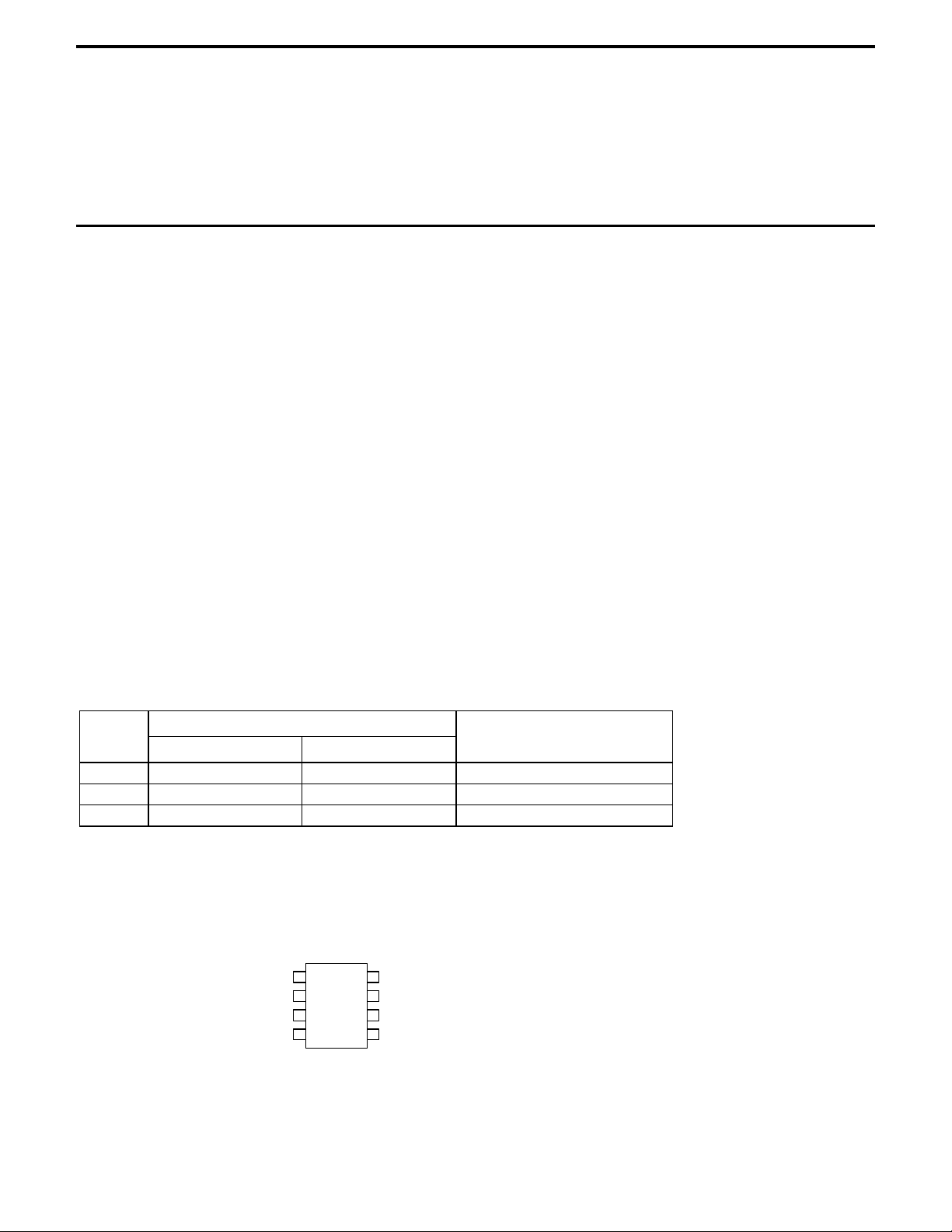
ORDERING INFORMATION:
TOL. PACKAGE TYPE OPERATING
TEMPERATURE RANGE
-40 to 85° C
-40 to 85° C
-40 to 85° C
±75µV
±150µV
±150µV
8 LEAD SOIC 8 LEAD PDIP
AMSOP-07ES AMSOP-07EP
AMSOP-07CS AMSOP-07CP
AMSOP-07DS AMSOP-07DP
PIN CONNECTIONS
8 Lead SOIC/ 8Lead PDIP
VOS TRIM
+IN
-IN
1
2
3
4
V-
8
VOS TRIM
7
V+
6 OUT
5
N/C
Top View
Advanced Monolithic Systems, Inc. 6680B Sierra Lane, Dublin, CA 94568 Phone (925) 556-9090 Fax (925) 556-9140

AMSOP-07
ABSOLUTE MAXIMUM RATINGS (Note1)
Supply Voltage
Differential Input Voltage
Input Voltage
±22V
±30V
±22V
Output Short Circuit Duration Indefinite Thermal Resistance
Operating Temperature Range
-40°C to 85°C
Storage temperature
Junction Temperature
Soldering information (60 sec)
8 L SOIC
8 L PDIP
-65°C to +125°C
+150°C
300°C
158°C/W
103°C/W
ELECTRICAL CHARACTERISTICS
Electrical Characteristics at VIN =±15V and TA = +25°C unless otherwise specified.
Parameter Conditions AMSOP-07E AMSOP-07 C AMSOP-07 D Units
Min Typ Max Min Typ Max Min Typ Max
Input Offset Voltage (Note 2) 30 75 60 150 60 150
Long Term V
Stability
Input Offset Current 0.5 3.8 0.8 6.0 0.8 6.0 nA
OS
(Note 3) 0.3 1.5 0.4 2.0 0.5 3.0
µV
µV/Mo
Input Bias Current
Input Noise Voltage
Input Noise Voltage
Density
Input Noise Current 0.1Hz to 10Hz 14 30 15 35 15 35 pA
Input Noise
CurrentDensity
Input Resistance
Differential-Mode
Input Resistance
Common-Mode
Input Voltage Range
Common-Mode
Rejection Ratio
Power Supply
Rejection Ratio
Large-Signal
Voltage Gain
Output Voltage
Swing
Slew Rate
Closed-Loop
Bandwidth
Open-Loop Output
Resistance
0.1Hz to 10Hz 0.35 0.6 0.38 0.65 0.38 0.65
fO = 10Hz
fO = 100Hz (Note 4)
fO = 1000Hz
fO = 10Hz
fO = 100Hz (Note 4)
fO = 1000Hz
(Note 5) 15 50 8 33 7 31
± 13 ± 14 ± 13 ± 14 ± 13 ± 14
VCM = ± 13
VS = ± 13 to ± 18
RL≥2kΩ, VO =± 10V
RL≥500Ω, VO =± 0.5V,
VS =± 0.5V (Note 5)
RL ≥10kΩ
RL ≥2kΩ
RL ≥1kΩ
RL ≥2kΩ (Note 4)
A
=+1
VCL
(Note 6)
VO = 0, IO= 0 60 60 60
106 123 100 120 94 110 dB
200
150
± 12.5
± 12.0
± 10.5
0.1 0.3 0.1 0.3 0.1 0.3
0.4 0.6 0.4 0.6 0.4 0.6 MHz
± 1.2 ± 4.0 ± 1.8 ± 7.0 ± 2.0 ± 12
10.3
10.0
9.6
0.32
0.14
0.12
160 120 120
5 20 7 32 7 32
500
400
± 13.0
± 12.8
± 12.0
18.0
13.0
11.0
0.80
0.23
0.17
120
100
± 12.0
± 11.5
10.5
10.2
9.8
0.35
0.15
0.13
400
400
± 13.0
± 12.8
± 12.0
20.0
13.5
11.5
0.90
0.27
0.18
120 400
± 12.0
± 11.5
± 13.0
± 12.8
± 12.0
10.5
10.3
9.8
0.35
0.15
0.13
400
20.0
13.5
11.5
0.90
0.27
0.18
µV
nV/√Hz
pA/√Hz
µV/V
V/mV
V/µs
nA
P-P
P-P
MΩ
GΩ
V
V
Ω
Power Consumption
Offset Adjustment
Range
VS =± 15V, No Load
VS =± 3V, No Load
RP =20kΩ ± 4 ± 4 ± 4
75
120
4
6
80
150
4
8
80
150
4
8
Advanced Monolithic Systems, Inc. 6680B Sierra Lane, Dublin, CA 94568 Phone (925) 556-9090 Fax (925) 556-9140
mW
mV
 Loading...