ADMOS AMS36063S, AMS36063P Datasheet

Advanced AMS36063
Monolithic DC-TO-DC CONVERTER CONTROL CIRCUIT
Systems
PRELIMINARY INFORMATION
FEATURES APPLICATIONS
•• Wide Input Voltage Operating Range from 2.5V to 60V •• Step-Up Converter
•• Low Standby Current •• Step-Down Converter
•• Current Limiting •• Voltage Inverting Application
•• Output Switch Current of 1.5A •• Telephone Circuits
•• Output Voltage Adjustable from 1.25 to 40V •• Monitors
•• Frequency of Operation to 100kHz ••Battery Chargers
•• Thermal Protection •• Portable Equipment
•• Enable Input Pin
GENERAL DESCRIPTION
The AMS36063 series is a control circuit containing the basic functions required for DC-to-DC converters. The device consists
of an internal temperature compensated reference, a comparator, a controlled duty cycle oscillator with an active current limit
circuit, a driver, a high current output switch, a thermal protection circuit and a converter enable input. Designed specifically to
be incorporated in Step-Up, Step-Down and Voltage -Inverting applications, the AMS36063 requires a minimum number of
external components.
The AMS36063 is available in the 8-lead plastic SOIC and 8-lead plastic DIP packages.
ORDERING INFORMATION
PACKAGE TYPE OPER. TEMP
8 LEAD PDIP 8 LEAD SOIC
AMS36063P AMS36063S
RANGE
-40°C to +85°C
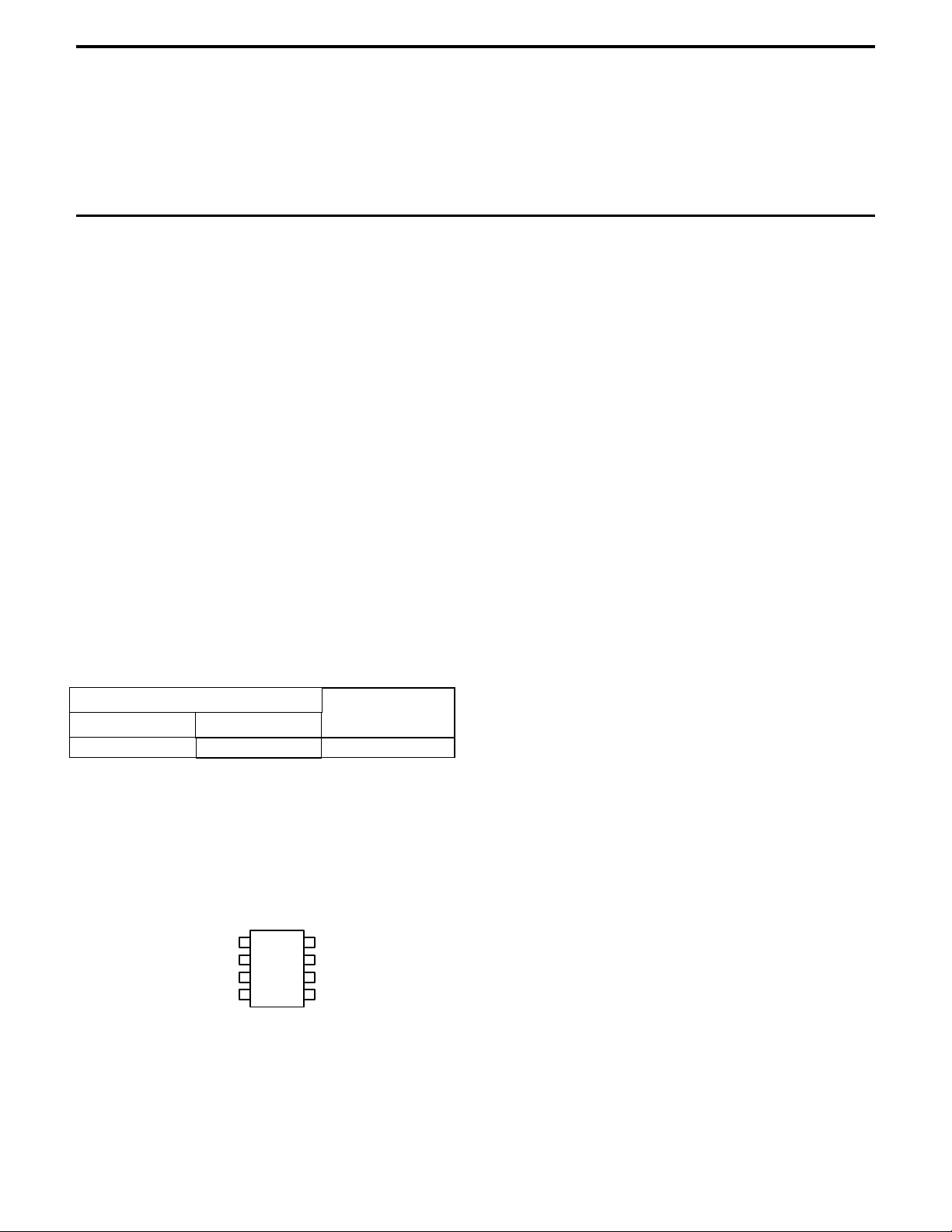
PIN CONNECTIONS
8 LEAD SOIC/ 8 LEAD PDIP
SWITCH
COLLECTOR
SWITCH
EMITTER
TIMING
CAPACITOR
GND
1
2
3
4
ENABLE
8
IPK SENSE
7
6
V
CC
COMPARATOR
5
INVERTING
INPUT
Top View
Advanced Monolithic Systems, Inc. 6680B Sierra Lane, Dublin, CA 94568 Phone (925) 556-9090 Fax (925) 556-9140

ABSOLUTE MAXIMUM RATINGS (Note 1)
Power Supply Voltage, V
Comparator Input Voltage Range, V
Switch Collector Voltage, V
Switch Emitter Voltage, V
CC
IR
C(switch)
E(switch)
Switch Collector to Emitter Voltage, V
-0.3V to +60V Switch Current, I
CE(switch)
60V Driver Collector Voltage, V
60V Power Dissipation (Note 3)
60V Maximum Junction Temperature
60V Storage Temperature
ELECTRICAL CHARACTERISTICS
Electrical Characteristics at VCC = 5.0V, -40°C ≤TA ≤+85°C, unless otherwise noted.
SW
C(driver)
AMS36063
60V
1.5A
+125°C
-65°C to +150°C
PARAMETER CONDITIONS
Min.
Oscillator
Charging Current
Discharge Current
Voltage Swing
Discharge to Charge Current
Ratio
Current Limit Sense Voltage
Output Switch (Note 2)
Saturation Voltage, Darlington
Connection
Saturation Voltage
DC Current Gain
Collector Off-State Current
Comparator
Threshold Voltage 1.18 1.25 1.32 V
Threshold Voltage Line
Regulation
Input Bias Current VIN = 0V 40 400 nA
Total Device
ENABLE Low
5.0V ≤ VCC ≤ 60V, TA= 25°C
5.0V ≤ VCC ≤ 60V, TA= 25°C
TA= 25°C
I
= VCC, TA= 25°C
PK(sense)
I
= I
CHG
ISW = 1.0A, V
ISW = 1.0A, I
ISW = 1.0A, V
V
CE
3.0V ≤ VCC ≤ 60V
3.0V ≤ VCC ≤ 60V
, TA= 25°C
DISCHG
C(driver)
= 50mA, (Forced β ≈ 20)
C(driver)
= 5.0V, TA= 25°C
CE
= 60V, TA= 25°C
= V
C(switch)
20 35 50
150 200 250
250 300 350 mV
AMS36063
Typ.
0.5 V
6.0 _
1.0 1.3 V
0.45 0.7 V
35 120
10 nA
0.04 0.2 mV/V
2.15 1.90 V
Max.
Units
µA
µA
P-P
ENABLE Low
Supply Current
Note 1: Absolute Maximum Ratings are limits beyond which damage to the device may occur. For guaranteed performance limits and associated test
conditions, see the Electrical Characteristics tables.
Note 2: To minimize power dissipation, low duty cycle pulse testing is used.
Note 3: Power dissipation at TA = 25°C is equal to 1.0W for the 8 lead P DIP package and 625mW for the SO-8 package. For operation at temperatures above
TA = 25°C derate the power dissipation at 10mW/°C.
3.0V ≤ VCC ≤ 60V
5.0V ≤ VCC ≤ 60V, I
CT = 0.001µF, V pin 5 > Vth,
Pin 2 = Gnd, Remaining pins open
PK(sense)
= VCC ,
2.50 2.26 V
2.4 4.0 mA
Advanced Monolithic Systems, Inc. 6680B Sierra Lane, Dublin, CA 94568 Phone (925) 556-9090 Fax (925) 556-9140
 Loading...