

Page 1

VPX6000 Series
Performance Rugged Conduction Cooled
6U VPX 4th Gen Intel® Core™ i7
Processor Blade
Manual Rev.: 0.10 preliminary
Revision Date: May 20, 2014
Part No: 50-15097-1000
Advance Technologies; Automate the World.
Page 2
Revision History
Revision Release Date Description of Change(s)
0.10 20/05/2014 Preliminary release
ii Revision History
Page 3

VPX6000
Preface
Copyright 2014 ADLINK Technology Inc.
This document contains proprietary infor mation protected by copyright. All rights are reserved. No part of this manual may be reproduced by any mechanical, electronic, or other means in any form
without prior written permission of the manufacturer.
Disclaimer
The information in this document is subject to change without prior
notice in order to improve reliability, design, and function and does
not represent a commitment on the part of the manufa cturer.
In no event will the manufacturer be liable for direct, indirect, special, incidental, or consequential damages arising out of the use or
inability to use the product or documentation, even if advised of
the possibility of such damages.
Environmental Responsibility
ADLINK is committed to fulfill its social responsibility to global
environmental preservation through compliance with the European Union's Restriction of Hazardous Substances (RoHS) directive and Waste Electrical and Electronic Equipment (WEEE)
directive. Environmental protection is a top priority for ADLINK.
We have enforced measures to ensure that our products, manufacturing processes, components, and raw materials have as little
impact on the environment as possible. When products are at their
end of life, our customers are encouraged to dispose of them in
accordance with the product disposal and/or recovery programs
prescribed by their nation or company.
Trademarks
Product names mentioned herein are used for identification purposes only and may be trademarks and/or registered trademarks
of their respective companies.
Preface iii
Page 4

Using this Manual
Audience and Scope
The VPX6000 User’s Manual is intended for hardware technicians
and systems operators with knowledge of installing, configuring
and operating industrial grade computer systems.
Manual Organization
This manual is organized as follows:
Chapter 1, Introduction: Introduces the VPX6000, its features,
block diagrams, and package contents.
Chapter 2, Specifications: Presents detailed specification infor-
mation.
Chapter 3, Functional Description: Describes the VPX6000
main functions.
Chapter 4, Board Interfaces: Describes the VPX6000 board
interfaces.
Important Safety Instructions: Presents safety instructions all
users must follow for the proper setup, installation and usage of
equipment and/or software.
Getting Service: Contact information for ADLINK’s worldwide
offices.
iv Preface
Page 5
VPX6000
Conventions
Take note of the following conventions used throughout this
manual to make sure that users perform certain tasks and
instructions properly.
Additional information, aids, and tips that help users perform
tasks.
NOTE:
NOTE:
Information to prevent minor physical injury, component damage, data loss, and/or program corruption when trying to com-
CAUTION:
WARNING:
plete a task.
Information to prevent serious physical injury, component
damage, data loss, and/or program corruption when trying to
complete a specific task.
Preface v
Page 6

This page intentionally left blank.
vi Preface
Page 7

VPX6000
Table of Contents
Revision History...................................................................... ii
Preface.................................................................................... iii
List of Figures........................................................................ ix
List of Tables.......................................................................... xi
1 Introduction ........................................................................ 1
1.1 Overview.............................................................................. 1
1.2 Features............................................................................... 2
1.3 Functional Block Diagrams.................................................. 3
1.4 Model Number Decoder - Processor Blade........................ 6
1.5 Package Contents ............................................................... 7
2 Specifications..................................................................... 9
2.1 VPX6000 Blade Specifications ............................................ 9
2.2 VPX-R6000 RTM Specifications........................................ 11
2.3 Power Consumption ............................... ... ... ..................... 12
3 Functional Description .................................................... 13
3.1 Processors......................................................................... 13
3.2 Chipset............................................................................... 15
3.3 Intel® Turbo Boost Technology......................................... 16
3.4 Intel® Hyper Threading Technology.................................. 16
3.5 Real Time Clock ................................................................ 16
4 Board Interfaces............................................................... 17
4.1 VPX6000 Board Layout ..................................................... 17
4.2 VPX6000 Onboard Connector Pin Assignments .............. . 19
4.3 VPX6000 VPX Connector Pin Assignments...................... 22
4.4 tBP-VPX6000 Board Layout .............................................. 35
Table of Contents vii
Page 8

4.5 tBP-VPX6000 Connector Pin Assignments ....................... 38
4.6 tBP-VPX6000 Switches and Jumpers................................ 45
Important Safety Instructions............................................... 47
Getting Service...................................................................... 49
viii Table of Contents
Page 9

VPX6000
List of Figures
Figure 1-1: VPX6000 Functional Block Diagram................................ 3
Figure 1-2: VPX-R6000 RTM Functional Block Diagram...................4
Figure 1-3: tBP-VPX6000 Test Backplane Block Diagram ................ 5
Figure 4-1: VPX6000 Board Layout - Top View...............................17
Figure 4-2: VPX6000 Front IO .........................................................17
Figure 4-3: VPX6000 Board Layout - Back View ............................. 18
Figure 4-4: tBP-VPX6000 Board Layout - Front View...................... 35
Figure 4-5: tBP-VPX6000 Board Layout - Rear View ......................36
List of Figures ix
Page 10

This page intentionally left blank.
xList of Figures
Page 11

VPX6000
List of Tables
Table 2-1: VPX6000 Blade Specifications........................................ 9
Table 2-2: VPX-R6000 RTM Specifications.................................... 11
Table 2-3: VPX6000 Power Consumption...................................... 12
Table 4-1: P1 Connector Signal Descriptions................................. 24
Table 4-2: P2 Connector Signal Descriptions................................. 26
Table 4-3: P3 Connector Signal Descriptions................................. 28
Table 4-4: P4 Connector Signal Descriptions................................. 30
Table 4-5: P5 Connector Signal Descriptions................................. 32
Table 4-6: P6 Connector Signal Descriptions................................. 34
Table 4-7: tBP-VPX6000 Signal Routing Table.............................. 37
List of Tables xi
Page 12

This page intentionally left blank.
xii List of Tables
Page 13

1 Introduction
1.1 Overview
The VPX6000 is a dual-CPU 4th Generation Intel® Core™ i7 processor 6U VPX blade (0.85" pitch) with Mobile Intel® QM87
Express Chipset in a rugged conduction cooled, VPX REDI (VITA
48) form factor. The VPX6000 features two CPU sub-systems,
each with up to 16GB DDR3-1600 dual channel ECC memory soldered onboard and onboard soldered 32GB SLC SATA solid state
drive. Rear I/O per node includes 2x 10GbE, 2x 1000BASE-BX
and 2x 1000BASE-T, 2x PCIe x1, HD audio (Line-in, Line-out), 3x
SATA 6 Gb/s, 2x USB 3.0, 2x USB 2.0, 8x GPIO, HDMI, DVI and
RS-232/422.
A VPX-R6000 Rear Transition Module is available to access rear
I/O signals from the VPX6000 and a tBP-VPX6000 Test Backplane
supporting three payload slots is available for users to validate
VPX6000 functionality.
The VPX6000 Series is rugged conduction cooled with conformal
coating, making it ideal for mission critical applications such as
military and aerospace platforms.
VPX6000
Introduction 1
Page 14

1.2 Features
X 6U VPX VITA 46, OpenVPX VITA 65, VPX REDI (VITA 48)
X Rugged conduction cooled 0.85" pitch 6U VPX blade with con-
formal coating
X Two CPU sub-systems: Node A, Node B
X 4th generation Intel® Core™ i7-4700EQ Processor
(4 cores, 6M L3 cache, 2.4/1.7 GHz, 47/37W TDP)
X Dual channel DDR3L-1600 SDRAM with ECC, 16 GB per node
X Intel® QM87 Chipset
X Intel® HD Graphics 4600 with DX11.1 and OCL 1.2
X Onboard 32GB SLC mode SATA flash by mezzanine card; 3x
SATA 6Gb/s to rear P3/P4, P5/P6 per CPU
X Graphics (each node):
Z 1x analog VGA port to front panel
Z 2x DVI/HDMI routed to rear (P5 for CPU-A, to P6 for
CPU-B)
Z Supports three independent displays
X I/O Ports (each node):
Z 2x 10GbE, 2x 1000BASE-T, 2x 1000BASE-KX
Z 2x USB 3.0, 2x USB 2.0, 3x SATA 6Gb/s
Z 2x RS-232/422/485 serial ports, 8x GPIO, PS/2 key-
board & mouse
X Expansion (with 2 nodes):
Z 1x PCIe x16 or 2x PCIe x8 or 4x PCIe x4 to P2 (Gen2)
Z 4x PCIe x1 to P3/P4
X uEFI BIOS 16MB flash
X Module profile: MOD6-PAY-4F1Q2U2T-12.2.1-8
X Slot Profile SLT6-PAY-4F1Q2U2T-10.2.1
2Introduction
Page 15
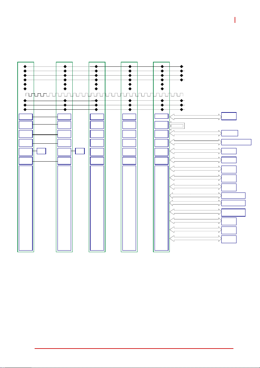
1.3 Functional Block Diagrams
VPX6000
I/O
expander
8x GPIO
PCIe x1
PCIe x1
P3
32GB Flash
SATA0
TPM
COM
IPMC
I2C
8x GPIO
P0
Front Panel
VGA
BIOS
SPI
PCH Node A
LPC
SIO
2x USB 3.0
1x SATA 6Gb/s
PS/2 KB/MS
P5
Gen2
DDR3L-1600
DDR3L-1600
DVI/HDMI
PCIe x8
or
PCIe x8
10GbE
ConnectX-3
1000BASE-KX/BX
1000BASE-T
2x USB 2.0
USB 3.0
2x SATA 6Gb/s
Audio, PS/2
PCIe x4
82580
2x COM
DDR3L-1600
DDR3L-1600
DVI/HDMI
CPU Node A CPU Node B
PCIe x8
PCIe x1
PHY
I271
iAMT
10GbE
ConnectX-3
PCIe Switch
PCIe x8
4x PCIe x4
2x PCIe x8
P1 P1P2
1000BASE-KX/BX
1000BASE-T
1000BASE-T
1000BASE-T
P5 Front P4
Figure 1-1: VPX6000 Functional Block Diagram
P6
1000BASE-T
PCIe x1
PHY
I271
iAMT
1000BASE-BX/KX 4
Front Panel
PCIe x4
82580
P6
USB 3.0
VGA
BIOS
SPI
PCH Node B
2x USB 2.0
2x SATA 6Gb/s
Audio, PS/2
2x COM
32GB Flash
SATA0
LPC
SIO
2x USB 3.0
1x SATA 6Gb/s
PS/2 KB/MS
PCIe x1
PCIe x1
TPM
P4
I/O
expander
8x GPIO
Introduction 3
Page 16
RP0
RP1
RP2
RP3
RP4
VS1(DC12V)
VS2(DC12V)
VS3(DC5V)
DC3V_AUX
NVMRO, SYSRESET#, JTAG
SM[0:1] IPM2, SM [2:3] I2C
10GbE
10GbE
PCIe x8
PCIe x8
USB 3.0 + USB 2.0
SATA 6 Gb/s
GPIO signal
PS/2 signal
PCIe x1
PCIe x1
1000BX 1000BX
USB 3.0 + USB 2.0
SATA 6 Gb/s
GPIO signal
PS/2 signal
10/100/1000BASE-T RJ-45
2x InfiniBand connectors
MASK_RESET
32NT8A_SMB
2x InfiniBand connectors
IPMC debug, SW EEPROM
CN34
board-to-board
connector
KB/MS
SPI Flash Socket
IPMC JTAG
BIOS_SEL
NA_CLK_PCIE_REAR
CN34
board-to-board
connector
KB/MS
2 ports
SPI Flash Socket NB
NB_CLK_PCIE_REAR
TPS53318DQPR
CN33
board-to-board
connector
CN33
board-to-boar d
connector
SATA
1 port
GPIO
LED X 8
CN34
board-to-board
connector
CN34
board-to-board
connector
2 port
SATA
1 port
GPIO
LED x8
NA+NB
NA
NA
NA
NA+NB
NB
NB
NB
NA+NB
P3V3, 4A
NA+NB
NA
USB 3.0 + USB 2.0
NA
NB
RP5
NA
NA
NB
Serial Port
SATA 6 Gb/s
10/100/1000BASE-T
1000BX
HDMI signal
HDMI signal
Audio signal
NA_BP_PWRBTN-L
USB 3.0 + USB 2.0
Serial Port
SATA 6 Gb/s
10/100/1000BASE-T
RP6
NB
1000BX
HDMI signal
HDMI signal HDMI 1 port
Audio signal
NB_BP_PWRBTN-L
USB
3 ports
RS-232/422
NA
2 port
SATA
NA
2 port
CN34
board-to-boa rd
connector
CN34
board-to-boa rd
connector
CN34
board-to-boa rd
connector
HDMI 1 port
Audio connector
NB
USB
3 port
RS-232/422
NB
2 port
SATA
NB
2 port
CN34
board-to-boa rd
connector
CN34
board-to-boa rd
connector
CN34
board-to-boa rd
connector
Audio connector
NA
NA
NA
NA
NA
NB
NB
NB
NB
NB
Figure 1-2: VPX-R6000 RTM Functional Block Diagram
4Introduction
Page 17
2x PCIe by 8
1000BASE
-BX X4
Intel 82580
1000BASE-T
X2
X4
Node A
Intel i217
1000BASE-T
Node B
Intel i217
1000BASE-T
KVM I/O
Crossover
Crossover
Crossover
Crossover10GBe
Crossover
2x PCIe by 8
1000BASE
-BX X4
Intel 82580
1000BASE-T
X2
10GBe
X4
Node A
Intel i217
1000BASE-T
Node B
Intel i217
1000BASE-T
KVM I/O
VPX6000
Slot#4 5#tolS3#tolSSlot#2Slot#1
VS1(DC12V), 32A/slot
VS2(DC12V), 32A/slot
VS3(DC5V), 23A/slot
DC3V_AUX,1A/Slot
REF_CLK+/-
SM[0:1] IPM2, SM[2:3] I2C
NVMRO, SYSRESET#, JTAG
VBAT
2x PCIe by 8
1000BASE
-BX X4
Intel 82580
1000BASE-T
X2
10GBe
X4
Node A
RJ45RJ45
Intel i217
1000BASE-T
Node B
Intel i217
1000BASE-T
KVM I/O
2x PCIe by 8
1000BASE
-BX X4
Intel 82580
1000BASE-T
X2
10GBe
X4
Node A
Intel i217
1000BASE-T
Node B
Intel i217
1000BASE-T
KVM I/O
2x PCIe by 8
1000BASE
-BX X4
Intel 82580
1000BASE-T
X2
10GBe
X4
Node A
Intel i217
1000BASE-T
Node B
Intel i217
1000BASE-T
KVM I/O
4x GbE 1000BASE-BX
Self loopback
2X 10/100/1000BASE-T
10GbE
10/100/1000BASE-T
10/100/1000BASE-T
SATA Gen3
USB 2.0
USB3.0 +USB2.0
DVI signal
HDMI signal
Audio signal
Serial Port
GPIO signal
PS/2 signal
XMC X2
RJ-45 jack X2
2x Infinit band connector
RJ-45 jack
RJ-45 jack
SATA3.0
6 port
USB2.0
4 port
USB3.0
4 port
DVI-I 2 port
HDMI 2 port
Audio jack(LI/LO)
2 port
RS-422
4 port
GPIO
LED X 16
KB/MS
Figure 1-3: tBP-VPX6000 Test Backplane Functional Block Diagram
Introduction 5
Page 18

1.4 Model Number Decoder - Processor Blade
V
PX6000/D4700/M64/S32-R1
(A) (B) (C) (D)
(A) CPU Code
Z S4700 = Single 4-core Intel® Core™ i7-4700EQ processor
Z D4700 = Dual 2-core Intel® Core™ i7-4700EQ processor
(B) Memory Size Code
Z M16 = Onboard 16GB DDR3L-1600 memory (Node A)
Z M32 = Onboard 32GB DDR3L-1600 memory (Node A + B)
(C) SA TA NAND Flash Size Code
Z S62 = Onboard 64GB (32GB per node)
(D) Ruggedized Level Code
Z R1 = Conduction cooled version supporting -40°C to +75°C
at card edge
Z R2 = Conduction cooled version supporting -40°C to +85°C
at card edge
Z A = Air cooled version supporting -40°C to +75°C
6Introduction
Page 19
VPX6000
1.5 Package Contents
The VPX6000 is packaged with the following components. If any
of the items on the contents list are missing or damaged, retain the
shipping carton and packing material and contact the dealer for
inspection. Please obtain authorization before returning any product to ADLINK. The packing contents of the VPX6000 are
non-standard configurations and may vary depending on customer
requests.
Processor Blade
X VPX6000
Z CPU and memory specifications will differ depending on
options selected
Z Thermal module is assembled on the board
X ADLINK Driver USB Flash Drive
Rear Transition Module
X VPX-R6000 RTM
Test Backplane
X tBP-VPX6000 test backplane
X DVI to VGA adapter
The contents of non-standard VPX6000 configurations may
vary depending on the customer requirements.
NOTE:
NOTE:
This product must be protected from static discharge and physical shock. Never remove any of the components except at a
CAUTION:
Introduction 7
static-free workstation. Use the anti-static bag shipped with the
product when putting the board on a surface. Wear an
anti-static wrist strap properly grounded on one of the system's
ESD ground jacks when installing or servicing system components.
Page 20

This page intentionally left blank.
8Introduction
Page 21

VPX6000
2 Specifications
2.1 VPX6000 Blade Specifications
Form Factor • 6U VPX VITA 46
• OpenVPX VITA 65
• VPX REDI (VITA 48)
Dual System • Two CPU sub-systems: Node A and Node B
(single node on S4700 SKU)
Processor • Quad-core Intel® Core™ i7-4700EQ processor,
2.4/1.7GHz, 6MB L3 cache, 47/37W TDP
Chipset • Intel® QM87 Chipset
VRD • VRM12.5 compliant
Memory • Dual channel DDR3L-1600 MHz with ECC soldered, max.
16GB (each node)
Data Transport
(each node)
Graphics • 1x analog VGA port to front panel
I/O Ports • 2x 10GbE
Expansion • 1x PCIe x16 or 2x PCIe x8 or 4x PCIe x4 (Gen2) from 32-
• Two Fat Pipes 10GbE to P1 for Data Plane by Mellanox
ConnectX-3
• Intel® 82580EB Quad GbE Controller on PCIe 2.0 x4
• Two 1000BASE-T to P4/P5 from Node A, two to P4/P6
from Node B
• Two 1000BASE-BX/KX to P4/P5 from Node A, two to
P4/P6 from Node B for Control Plane
• Intel® Ethernet Connection I217-LM, one GbE with Intel®
AMT to rear IO
• 2x DVI/HDMI routed to rear P5 for CPU-A, to P6 for CPU-B
• Three independent displays supported
• 2x 1000BASE-T
• 2x 1000BASE-KX
• 2x USB 3.0 ports
• 2x USB 2.0 ports
• 3x SATA 6Gb/s interface
• 2x RS-232/422/485 serial ports
•8x GPIO
• PS/2 keyboard mouse
lane PCIe switch to P2 (16 lanes per node)
• Four PCIe x1 ports to P3/P4 (2 lanes per node)
T a ble 2-1: VPX6000 Blade S p ecif ications
Specifications 9
Page 22

Audio • Stereo audio, single-ended Line-in, Line-out to RTM (each
node)
Super IO ITE IT8783E/AX-L (each node)
• 2 Serial ports
• Keyboard/Mouse routed to RTM
BIOS • AMI® EFI BIOS, SPI flash memory
• Dual failover BIOS per node
Storage
(each node)
Watchdog
Timer
GPIO • 8 GPIO pins per node routed to RTM
Miscellaneous • Front panel LEDs: CPU, PCH, RAM, P12V, P5V Power
Mechanical • Dimensions: 233.35 mm x 160 mm (0.85" pitch)
Environmental • Operating Temperature:
Operating
Systems
EMI • CE/FCC Class A
• One 32GB SLC mode SATA flash by mezzanine card
• Three SATA 6Gb/s to rear P3/P4 ,P5/P6
• System Reset and NMI, with programmable interval via
IPMC
Good, Port 80
• Recessed reset button
• Weight: 1407.3 g
ETT (R2): -40°C to +75°C air cooled
CC 1 (R1): -40°C to +75°C conduction cooled
CC 2 (R2): -40°C to +85°C conduction cooled
• Storage Temperature: -50°C to 100°C
• Humidity: 95%, non-condensing
• Shock:
ETT (R2): 20g peak, 11ms
CC 1/2 (R1/R2): 40g peak, 11ms
• Vibration:
ETT (R2): Random: 0.002G2/Hz, 10~2000Hz; Sine: 2G
5~500Hz
CC 1/2 (R1/R2): Random: 0.1G2/Hz, 15~2000Hz;
12Grms (MIL-STD-810F Fig 514.4-8 for aircraft)
• Conformal Coating:
ETT (R2): optional
CC 1/2 (R1/R2): default
• Microsoft Windows 7 32/64-bit
• Red Hat Enterprise Linux
• Wind River VxWorks 6.9.3
Table 2-1: VPX6000 Blade Specifications
Note: Specifications are subject to change without prior notice.
10 Specifications
Page 23

2.2 VPX-R6000 RTM Specifications
VITA Standards • VITA 46.10 Rear Transition Module on VPX
Mechanical • 233.35mm x 160mm
Front I/O • 2x 1000BASE-BX
• 2x 1000BASE-T; RJ-45 connectors
• 2x 10G Infiniband connectors
• 2xUSB 3.0 port
• 2x mini-HDMI connectors
• 1x Mini UART connector
Onboard
Interfaces
Note: Specifications are subject to change without prior notice.
• 2x 10G Infiniband connector
• 4x USB 2.0 headers
• 1x UART header
• 6x SATA connectors
• 2x EEPROM
•Battery
• 2x board-to-board connectors
Table 2-2: VPX-R6000 RTM Specifications
VPX6000
Specifications 11
Page 24

2.3 Power Consumption
This section provides information on the power consumption of the
VPX6000.
Te s t Configuration (Node A / Node B)
Processor Intel® Core™ i7-4700EQ Processor 2.4GHz
(6M L3 Cache)
Memory Channel 1 Onboard soldered memory 8GB
Memory Channel 2 Onboard soldered memory 8GB
Graphics Intel® HD Graphics 4600
Power Supply FSP FSP460-60PFG 460W ATX, 460W
OS / Mode* Power Consumption (W)
DOS
Windows 7, Idle Load
Windows 7, Typical Load
Windows 7, Max. Load
Table 2-3: VPX6000 Power Consumption
Notes*:
X Idle Load: Windows 7 login prompt
X Typical Load: Run BurnInTest to execute CPU, memory,
2D/3D graphics and video playback items
X Max. Load: Run Intel TAT for maximum power consumption
70.41
43.69
123.61
129.63
12 Specifications
Page 25

3 Functional Description
The following sections describe the VPX6000 features and
functions.
3.1 Processors
The 4th Generation Intel® Core™ i7 Processor is the next generation of 64-bit, multi-core mobile processors built on 22-nanometer
process technology. Based on a new micro-architecture, the processor is designed for a two-chip platform. The two-chip platform
consists of a processor and Platform Controller Hub (PCH). The
platform enables higher performance, lower cost, easier validation, and improved x-y footprint. The processor includes an integrated display engine, processor graphics, integrated memory
controller, and integrated I/O on a single silicon die.
Features Core™ i7-3612QE
Clock 2.4 GHz
Max. Single Core Turbo Freq. 3.4 GHz
Last Level Cache 6 MB
No. of Cores/Threads 4/8
Maximum Power (TDP
T
junction,MAX
2
1
)
47 W
100°C
VPX6000
Notes:
1. The highest expected sustainable po wer while running known
power intensive applications. TDP is not the maximum power
that the processor can dissipate.
2. The maximum supported operating temp erature.
Functional Description 13
Page 26

Supported Technologies
Z Intel® Virtualization Techno logy for Directed I/O (Intel®
VT-d)
X Intel® Virtualization Technology (Intel® VT-x)
X Intel® vPro Technology (Intel® VT)
X Intel® Trusted Execution Technology (Intel® TXT)
X Intel® Hyper-Threading Technology
X Intel® 64 Architecture
X Intel® Turbo Boost Technology 2.0
X AES New Instructions
X Intel® My WiFi Technology
X Enhanced Intel SpeedStep® Technology
X Thermal Monitoring Technologies
X Intel® Fast Memory Access
X Execute Disable Bit
X Intel® VT-x with Extended Page Tables (EPT)
Interfaces
X Dual channel DDR3L memory with one channel of unbuffered
SODIMM and one channel of soldered SDRAM
X Memory DDR3L data transfer rates of 1333 MT/s and 1600
MT/s
X 64-bit wide channels plus 8-bits of ECC support for each
channel
X System Memory Interface I/O Voltage of 1.5V
X 1-Gb, 2-Gb, and 4-Gb DDR3L DRAM technologies supported
Z Using 4Gb DRAM device technologies, the largest memory
capacity possible is 8 GB.
Z Intel Fast Memory Access:
Just-in-Time Command Scheduling
Command Overlap
Out-of Order Scheduling
X The PCI Express lanes are fully-compliant with the PCI
Express Base Specification, Revision 3.0, including support
for 8.0 GT/s transfer speeds.
14 Functional Description
Page 27

VPX6000
3.2 Chipset
The VPX6000 incorporates the Mobile Intel® QM87 Chipset
(Intel® DH82QM87 PCH).
Mobile Intel® QM87 Express Chipset
X PCI Express Base Specification, Revision 2.0 support for up
to eight ports with transfer rate up to 5 GT/s
X ACPI Power Management Logic Support, Revision 4.0a
X Enhanced DMA controller, interrupt controller, and timer
functions
X Integrated Serial ATA host controllers with independent
DMA operation on up to six port s SATA 3Gb/s and up to two
ports SATA 6.0 Gb/s
X Supports USB 2.0, USB 3.0
X USB host interface with two EHCI high-speed USB 2.0 Host
controllers and two rate matching hubs
X System Management Bus (SMBus) Specification, Version
2.0 with additional support for I
X Supports Intel® Trusted Execution Technology
X Support Intel® vPro Technology
X Supports Intel® High Definition Audio
X Supports Intel® Rapid Storage Technology
X Supports Intel® Virtualization Technology for Directed I/O
X Low Pin Count (LPC) interface
X Serial Peripheral Interface (SPI) support
2
C devices
Functional Description 15
Page 28

3.3 Intel® Turbo Boost Technology
Intel Turbo Boost Technology is a feature that allows the processor
to opportunistically and automatically run faster than its rated
operating core and/or render clock frequency when there is sufficient power headroom, and the product is within specified temperature and current limits. The Intel Turbo Boost Technology feature
is designed to increase performance of both multi-threaded and
single-threaded workloads. The processor supports a Turbo mode
where the processor can use the thermal capacity associated with
package and run at power levels higher than TDP power for short
durations. This improves the system responsiveness for short,
bursty usage conditions.
Turbo Mode availability is independent of the number of active
cores; however, the Turbo Mode frequency is dynamic and dependent on the instantaneous application power load, the number of
active cores, user configurable settings, operating environment,
and system design. If the power, current, or thermal limit is
reached, the processor will automatically reduce the frequency to
stay with its TDP limit.
3.4 Intel® Hyper Threading Technology
The processor supports Intel® Hyper-Threading Technology
(Intel® HT Technology), that allows an execution core to function
as two logical processors. While some execution resources (such
as caches, execution units, and buses) are shared, each logical
processor has its own architectural state with its own set of general-purpose registers and control registers. This feature must be
enabled using the BIOS and requires operating system support.
3.5 Real Time Clock
The Intel® QM87 PCH contains a Motorola MC146818B-compatible real-time clock (RTC) with 256 bytes of RAM. The real-time
clock performs two key functions: keeping track of the time of day
and storing system data. The RTC operates on a 32.768 KHz
crystal and is powered by P3V3_AUX or VBAT. There is no external RTC battery on the VPX6000 to power the RTC after the system is powered off.
16 Functional Description
Page 29

4 Board Interfaces
4.1 VPX6000 Board Layout
VPX6000
10GbE
Node A
DDR3L-1600
ECC
Node A
CPU
Node A
PCH
SATA SSD
B2B connector
Node A
VGA
P0 P1 P2 P3
Node A
XDP
Node A
GbE RJ45
Node A
USB 3.0
Node B
USB 3.0
P4
Figure 4-1: VPX6000 Board Layout - Top View
Node B
XDP
P5
Node B
GbE RJ45
P6
Quad GbE
IDT Switch
Super I/O
Node B
PCH
Node B
CPU
Node B
DDR3L-1600
ECC
Node B
VGA
Figure 4-2: VPX6000 Front IO
Board Interfaces 17
Page 30

P0
P2
P1
P3
P4
P5
P6
Alignment
Key 1
Wedge
Lock
Aluminum
Thermal
Module
Alignment Key 2
Handle
Status LEDs
Figure 4-3: VPX6000 Board Layout - Back View
Handle
Alignment
Key 3
Wedge
Lock
SSD
Module
18 Board Interfaces
Page 31

VPX6000
4.2 VPX6000 Onboard Connector Pin Assignments
USB 3.0 Connector (Node A: CN3; Node B: CN12)
Pin # Signal Name
1+5V
2 Data3Data+
4GND
5RX_N
6RX_P
7GND
8TX_N
9TX_P
DB-15 VGA Connector (Node A: CN1; Node B: CN6)
Signal Name Pin # Pin # Signal Name
Red 1 2 Green
Blue 3 4 N.C.
GND 5 6 GND
GND 7 8 GND
+5V. 9 10 GND
N.C. 11 12 CRTDATA
HSYNC 13 14 VSYNC
CRTCLK 15
Board Interfaces 19
Page 32

RJ-45 Gigabit Ethernet Connectors (CN9 and CN10)
Pin # 1000BASE-T
1BI_DA+
2BI_DA3BI_DB+
4BI_DC+
5BI_DC6BI_DB7BI_DD+
8BI_DD-
Speed
Status
Network link is not established
or system powered off
10 Mbps
100 Mbps
1000 Mbps
Link OFF ON
Active OFF Blinking
Link Green ON
Active Green Blinking
Link Orange ON
Active Orange Blinking
LAN LED Status Definitions
Activity
18
Speed LED
(Green/Yellow)
OFF OFF
Activity LED
(Green)
20 Board Interfaces
Page 33

Information LEDs
LED Ref Color Description
LED15 Blue Node A Vcore Power Good
LED13 Blue Node A PCH P1V5 Power Good
LED28 Yellow Node A Port 80 bit0
LED29 Yellow Node A Port 80 bit1
LED30 Yellow Node A Port 80 bit2
LED31 Yellow Node A Port 80 bit3
LED32 Yellow Node A Port 80 bit4
LED33 Yellow Node A Port 80 bit5
LED34 Yellow Node A Port 80 bit6
LED35 Yellow Node A Port 80 bit7
LED18 Blue Node B Vcore Power Good
LED16 Blue Node B PCH P1V5 Power Good
LED36 Yellow Node B Port 80 bit0
LED37 Yellow Node B Port 80 bit1
LED38 Yellow Node B Port 80 bit2
LED39 Yellow Node B Port 80 bit3
LED40 Yellow Node B Port 80 bit4
LED41 Yellow Node B Port 80 bit5
LED42 Yellow Node B Port 80 bit6
LED43 Yellow Node B Port 80 bit7
LED26 Green P5V Power Ready
LED27 Green P12V Power Ready
LED22 Green P3V3_AUX Power Ready
VPX6000
Board Interfaces 21
Page 34

4.3 VPX6000 VPX Connector Pin Assignments
P0 Connector Pin Assignment
Pin A B C D E F G
1 P12V P12V P12V NC P12V P12V P12V
2 P12V P12V P12V NC P12V P12V P12V
3 P5V P5V P5V NC P5V P5V P5V
4 NVMRO SYSTEM RESET GND NC GND I2C_DAT I2C_CLK
5 IPMC_DAT IPMC_CLK GND P3V3_AUX GND GA4 GAP
6 GA0 GA1 GND NC GND GA2 GA3
7 JTAG_TRST JTAG_TMS GND JTAG_TDI JTAG_TDO GND JTAG_TCK
8 GND NC NC GND REF_CLK+ REF_CLK- GND
Signal I/O Description
P12V I +12V power source
P5V I +5V power source
NVMRO I/O
SYSTEM RESET I/O System Reset, generally input, sourced by the system controller
NC ? Not Connected
I2C_DAT I/O Node A PCH SMBus data
I2C_CLK I/O Node A PCH SMBus clock
IPMC_DAT I/O IPMC I2C bus data
IPMC_CLK I/O IPMC I2C bus clock
P3V3_AUX I 3.3V auxiliary power
GPA/GA[0..4] I Geographical Address Inputs 0-4, Parity
JTAG_***** I/O JTAG signals for G-LAN and PCIE-LAN
REF_CLK+/- 0 Provide 25MHz reference clock when P1 SYS_CON is low
Non-Volatile Memory Read Only
Derived by the system controller/plug in module
22 Board Interfaces
Page 35

VPX6000
P1 Connector Pin Assignment
Pin A B C D E F G
NA_10G_
1
RX0_L0_P
2GND
NA_10G_
3
RX0_L2_P
4GND
NB_10G_
5
RX0_L0_P
6GND
NB_10G_
7
RX0_L2_P
8GND
NA_10G_
9
RX1_L0_P
10 GND
NA_10G_
11
RX1_L2_P
12 GND
NB_10G_
13
RX1_L0_P
14 GND
NB_10G_
15
RX1_L2_P
16 GND
NA_10G_
RX0_L0_N
NA_10G_
RX0_L1_P
NA_10G_
RX0_L2_N
NA_10G_
RX0_L3_P
NB_10G_
RX0_L0_N
NB_10G_
RX0_L1_P
NB_10G_
RX0_L2_N
NB_10G_
RX0_L3_P
NA_10G_
RX1_L0_N
NA_10G_
RX1_L1_P
NA_10G_
RX1_L2_N
NA_10G_
RX1_L3_P
NB_10G_
RX1_L0_N
NB_10G_
RX1_L1_P
NB_10G_
RX1_L2_N
NB_10G_
RX1_L3_P
GND
NA_10G_
RX0_L1_N
GND
NA_10G_
RX0_L3_N
GND
NB_10G_
RX0_L1_N
GND
NB_10G_
RX0_L3_N
GND
NA_10G_
RX1_L1_N
GND
NA_10G_
RX1_L3_N
GND
NB_10G_
RX1_L1_N
GND
NB_10G_
RX1_L3_N
NA_10G_
TX0_L0_P
GND
NA_10G_
TX0_L2_P
GND
NB_10G_
TX0_L0_P
GND
NB_10G_
TX0_L2_P
GND
NA_10G_
TX1_L0_P
GND
NA_10G_
TX1_L2_P
GND
NB_10G_
TX1_L0_P
GND
NB_10G_
TX1_L2_P
GND
NA_10G_
TX0_L0_N
NA_10G_
TX0_L1_P
NA_10G_
TX0_L2_N
NA_10G_
TX0_L3_P
NB_10G_
TX0_L0_N
NB_10G_
TX0_L1_P
NB_10G_
TX0_L2_N
NB_10G_
TX0_L3_P
NA_10G_
TX1_L0_N
NA_10G_
TX1_L1_P
NA_10G_
TX1_L2_N
NA_10G_
TX1_L3_P
NB_10G_
TX1_L0_N
NB_10G_
TX1_L1_P
NB_10G_
TX1_L2_N
NB_10G_
TX1_L3_P
GND
NA_10G_
TX0_L1_N
GND
NA_10G_
TX0_L3_N
GND
NB_10G_
TX0_L1_N
GND
NB_10G_
TX0_L3_P
GND
NA_10G_
TX1_L1_N
GND
NA_10G_
TX1_L3_N
GND
NB_10G_
TX1_L1_N
GND
NB_10G_
TX1_L3_N
NA_10G_
RX0_L0_P
GND
NA_10G_
RX0_L2_P
GND
NB_10G_
RX0_L0_P
GND
NB_10G_
RX0_L2_P
GND
NA_10G_
RX1_L0_P
GND
NA_10G_
RX1_L2_P
GND
NB_10G_
RX1_L0_P
GND
NB_10G_
RX1_L2_P
GND
Board Interfaces 23
Page 36

Signal I/O Description
BAT_CN I RTC battery power source
Rule 4-33: The SYS_CON* line shall indicate if the module
should or should not be the System Controller.
SYS_CON-L I
SYSBP_PWRBTN-L I
MASK_RESET-L I Makeable reset by software
NA_10G_TX[O/1]
_L[3:0][P/N]
NA_10G_RX[O/1]
_L[3:0][P/N]
NB_10G_TX[O/1]
_L[3:0][P/N]
NB_10G_RX[O/1]
_L[3:0][P/N]
O Node A 10GLAN transmit lane from payload to backplane
I Node A 10GLAN receive lane from backplane to payload
O Node B 10GLAN transmit lane from payload to backplane
I Node B 10GLAN receive lane from backplane to payload
SYS_CON* = grounded; indicates that this module
is the System Controller
SYS_CON* = open; indicates that this module
is not the System Controller.
Backplane Power Button. Drive low to assert
"power button", then system boot up.
Table 4-1: P1 Connector Signal Descriptions
24 Board Interfaces
Page 37

VPX6000
P2 Connector Pin Assignment
Pin A B C D E F G
PCIE_BP1_
1
RXP0
2GND
PCIE_BP1_
3
RXP2
4GND
PCIE_BP2_
5
RXP0
6GND
PCIE_BP2_
7
RXP2
8GND
PCIE_BP3_
9
RXP0
10 GND
PCIE_BP3_
11
12 GND
13
14 GND
15
16 GND
RXP2
PCIE_BP4_
RXP0
PCIE_BP4_
RXP2
PCIE_BP1_
RXN0
PCIE_BP1_
RXP1
PCIE_BP1_
RXN2
PCIE_BP1_
RXP3
PCIE_BP2_
RXN0
PCIE_BP2_
RXP1
PCIE_BP2_
RXN2
PCIE_BP2_
RXP3
PCIE_BP3_
RXN0
PCIE_BP3_
RXP1
PCIE_BP3_
RXN2
PCIE_BP3_
RXP3
PCIE_BP4_
RXN0
PCIE_BP4_
RXP1
PCIE_BP4_
RXN2
PCIE_BP4_
RXP3
GND
PCIE_BP1
_RXN1
GND
PCIE_BP1
_RXN3
GND
PCIE_BP2
_RXN1
GND
PCIE_BP2
_RXN3
GND
PCIE_BP3
_RXN1
GND
PCIE_BP3
_RXN3
GND
PCIE_BP4
_RXN1
GND
PCIE_BP4
_RXN3
PCIE_BP1_
TXP0
GND
PCIE_BP1_
TXP2
GND
PCIE_BP2_
TXP0
GND
PCIE_BP2_
TXP2
GND
PCIE_BP3_
TXP0
GND
PCIE_BP3_
TXP2
GND
PCIE_BP4_
TXP0
GND
PCIE_BP4_
TXP2
GND
PCIE_BP1_
TXN0
PCIE_BP1_
TXP1
PCIE_BP1_
TXN2
PCIE_BP1_
TXP3
PCIE_BP2_
TXN0
PCIE_BP2_
TXP1
PCIE_BP2_
TXN2
PCIE_BP2_
TXP3
PCIE_BP3_
TXN0
PCIE_BP3_
TXP1
PCIE_BP3_
TXN2
PCIE_BP3_
TXP3
PCIE_BP4_
TXN0
PCIE_BP4_
TXP1
PCIE_BP4_
TXN2
PCIE_BP4_
TXP3
GND NC
PCIE_BP1
_TXN1
GND NC
PCIE_BP1
_TXN3
GND NC
PCIE_BP2
_TXN1
GND NC
PCIE_BP2
_TXN3
GND
PCIE_BP3
_TXN1
GND
PCIE_BP3
_TXN3
GND
PCIE_BP4
_TXN1
GND
PCIE_BP4
_TXN3
GND
GND
GND
GND
IPMI_PRG
_RX
GND
IPMI_PRG
_TX
GND
32NT8A_M
SMBCLK
GND
32NT8A_M
SMBDAT
GND
Board Interfaces 25
Page 38

Signal I/O Description
IPMI_PRG_RX /
IPMI_PRG_TX
32NT8A_MSMBCLK /
32NT8A_MSMBDAT
PCIE_BP1_
[N/P]TX(3:0)
PCIE_BP1_
[N/P]RX(3:0)
PCIE_BP2_
[N/P]TX(3:0)
PCIE_BP2_
[N/P]RX(3:0)
PCIE_BP3_[
N/P]TX(3:0)
PCIE_BP3_
[N/P]RX(3:0)
PCIE_BP4_
[N/P]TX(3:0)
PCIE_BP4_
[N/P]RX(3:0)
I/O COM port for IMPC software develop
I/O I2C port for PCIE Switch Hub software develop
O PCIe channel A transmit lane from payload to backplane
I PCIe channel A receive lane from backplane to payload
O PCIe channel B transmit lane from payload to backplane
I PCIe channel B receive lane from backplane to payload
O PCIe channel C transmit lane from payload to backplane
I PCIe channel C receive lane from backplane to payload
O PCIe channel D transmit lane from payload to backplane
I PCIe channel D receive lane from backplane to payload
Table 4-2: P2 Connector Signal Descriptions
26 Board Interfaces
Page 39

VPX6000
P3 Connector Pin Assignment
Pin A B C D E F G
NA_REAR
1
-RXP1
2GND
NA_USB3_
3
RX_2P
4 GND NC NC GND
NA_SPI_SO_C2NA_SPI_
5
6GNDNA_MSCLK
NA_LPC_
7
8GND
9
10 GND
11 PROG_TDI PROG_TDO GND
12 GND
13 NC NC GND NC NC GND 13
14 GND NC NC GND NC NC 14
15
16 GND P12V P 12V GND P5V P5V 16
AD0
NA_USB3_
RX_5P
REAR_LANS
W_UART_TX
NA_REAR-R
XN1
NA_REAR-R
XP2
NA_USB3_
RX_2N
CS2#
NA_LPC_
AD1
NA_LPC_
FRAME-L
NA_USB3_R
X_5N
NA_SATA_R
XP3
PROG_TDO_
CTRL
REAR_LANS
W_UART_RX
GND
NA_REAR-
RXN2
GND
GND
NA_MSDA
TA
GND
NA_CLK33
_DBC
GND
NA_SATA_
RXN3
NC GND NC NC 12
GND NC NC GND 15
NA_REAR
-TXP1
GND
NA_USB3
_TX_2P
NA_SPI_
SI_C2
GND NA_KBCLK
NA_LPC_
AD2
GND NC
NA_USB3
_TX_5P
GND
PROG_TMSPROG_JTA
NA_REAR-T
XN1
NA_REAR-T
XP2
NA_USB3_T
X_2N
NA_RTM_
BOOT#
NA_SPI_
CLK_C2
NA_LPC_
AD3
NA_USB3_T
X_5N
NA_SATA_T
XP3
G_VPX_TCK
GND
NA_REAR
-TXN2
GND
NA_EXT_
NODE_RST
GND
NA_KB
DATA
GND
NA_PLTRS
T_BIOS-L
GND 9
NA_SATA_
TXN3
GND 11
NA_REAR
-RXP1
GND
NA_USB3
_RX_2P
GND
NA_SPI_S
O_C2
GND
NA_LPC_
AD0
GND
10
Board Interfaces 27
Page 40

Signal I/O Description
NA_REAR-RX[P/N]1 I Node A PCIe port1 receive LAN from backplane to PCH
NA_REAR-TX[P/N]1 O Node A PCIe port1 transmit LAN from PCH to backplane
NA_REAR-RX[P/N]2 I Node A PCIe port2 receive LAN from backplane to PCH
NA_REAR-TX[P/N]2 O Node A PCIe port2 transmit LAN from PCH to backplane
NA_REAR_GPIO[0:7] I/O Node A General Purpose IO, Channels 0-7
NA_USB3_RX_2[P/N] I Node A USB 3.0 port receive lane from backplane to PCH
NA_USB3_TX_2[P/N] O Node A USB 3.0 port transmit lane from PCH to backplane
NA_USB3_RX_5[P/N] I Node A USB 3.0 port receive lane from backplane to PCH
NA_USB3_TX_5[P/N] O Node A USB 3.0 port transmit lane from PCH to backplane
NA_RTM_BOOT# I Node A boot up from RTM BIOS when this pin pull low
NA_EXT_NODE_RST I Node A reset input
NA_SATA_RX[P/N]3 I Node A SATA 6Gb/s port receive lane from backplane to PCH
NA_SATA_TX[P/N]3 O Node A SATA 6Gb/s port transmit lane from PCH to backplane
NA_SPI_* I/O Node A SPI bus for RTM BIOS
NA_LPC_* I/O Node A LPC bus for RTM debug port
NA_MSCLK I/O Node A PS2 bus mouse signal clock
NA_MSDATA I/O Node A PS2 bus mouse signal data
NA_KBCLK I/O Node A PS2 bus keyboard signal clock
NA_KBDATA I/O Node A PS2 bus keyboard signal data
PROG_* I/O IPMC JTAG PORT
REAR_LANSW_UART_TX /
REAR_LANSW_UART_RX
P12V I +12V Power source
P5V I +5V Power source
I/O COM port for GLAN Switch hub software develop
Table 4-3: P3 Connector Signal Descriptions
28 Board Interfaces
Page 41

VPX6000
P4 Connector Pin Assignment
Pin A B C D E F G
NB_REAR-
1
RXP1
2GND
NB_USB3_
3
RX_2P
4 GND NC NC GND
NB_SPI_S
5
O_C2
6GND
NB_LPC_AD0NB_LPC_A
7
8GND
NB_USB3_
9
RX_5P
10 GND
NB_GLAN_
11
KXR0_P
12 GND
13 MXA1-P MXA1-N GND MXB1-P MXB1-N GND MXA1-P
14 GND MXC1-P MXC1-N GND MXD1-P MXD1-N GND
15 MXA0-P MXA0-N GND MXB0-P MXB0-N GND MXA0-P
16 GND MXC0-P MXC0-N GND MXD0-P MXD0-N GND
NB_REAR-
RXN1
NB_REAR-
RXP2
NB_USB3_
RX_2N
NB_SPI_
CS2#
NB_MS
CLK
D1
NB_LPC_
FRAME-L
NB_USB3_
RX_5N
NB_SATA_
RXP3
NB_GLAN_
KXR0_N
NA_GLAN_
KXR0_P
GND
NB_REAR-
RXN2
GND
GND
NB_MSDA
TA
GND
NB_CLK33
_DBC
GND
NB_SATA_
RXN3
GND
NA_GLAN
_KXR0_N
NB_REAR-
TXP1
GND
NB_USB3_
TX_2P
NB_SPI_SI
_C2
GND NB_KBCLK
NB_LPC_AD2NB_LPC_A
GND NC
NB_USB3_
TX_5P
GND
NB_GLAN
_KXT0_P
GND
NB_REAR-
TXN1
NB_REAR-
TXP2
NB_USB3_
TX_2N
NB_RTM_
BOOT#
NB_SPI_C
LK_C2
D3
NB_USB3_
TX_5N
NB_SATA_
TXP3
NB_GLAN_
KXT0_N
NA_GLAN_
KXT0_P
GND
NB_REAR-
TXN2
GND
NB_EXT_
NODE_RST
GND
NB_KBDAT
A
GND
NB_PLTRS
T_BIOS-L
GND
NB_SATA_
TXN3
GND
NA_GLAN_
KXT0_N
NB_REAR-
RXP1
GND
NB_USB3_
RX_2P
GND
NB_SPI_
SO_C2
GND
NB_LPC_
AD0
GND
NB_USB3_
RX_5P
GND
NB_GLAN
_KXR0_P
GND
Board Interfaces 29
Page 42

Signal I/O Description
NB_REAR-RX[P/N]1 I Node B PCIe port1 receive lan from backplane to PCH
NB_REAR-TX[P/N]1 O Node B PCIe port1 transmit lan from PCH to backplane
NB_REAR-RX[P/N]2 I Node B PCIe port2 receive LAN from backplane to PCH
NB_REAR-TX[P/N]2 O Node B PCIe port2 transmit LAN from PCH to backplane
NB_REAR_GPIO[0:7] I/O Node B General Purpose IO, Channels 0-7
NB_USB3_RX_2[P/N] I Node B USB 3.0 port receive lane from backplane to PCH
NB_USB3_TX_2[P/N] O Node B USB 3.0 port transmit lane from PCH to backplane
NB_USB3_RX_5[P/N] I Node B USB 3.0 port receive lane from backplane to PCH
NB_USB3_TX_5[P/N] O Node B USB 3.0 port transmit lane from PCH to backplane
NB_RTM_BOOT# I Node B boot up from RTM BIOS when this pin pull low
NB_EXT_NODE_RST I Node B reset input
NB_SATA_RX[P/N]3 I Node B SATA 6Gb/s port receive lane from backplane to PCH
NB_SATA_TX[P/N]3 O Node B SATA 6Gb/s port transmit lane from PCH to backplane
NB_SPI_* I/O Node B SPI bus for RTM BIOS
NB_LPC_* I/O Node B LPC bus for RTM debug port
NB_MSCLK I/O Node B PS2 bus mouse signal clock
NB_MSDATA I/O Node B PS2 bus mouse signal data
NB_KBCLK I/O Node B PS2 bus keyboard signal clock
NB_KBDATA I/O Node B PS2 bus keyboard signal data
MX[A:D]0-[P/N] I/O Node A 1Gb BASE-T Ethernet
MX[A:D]1-[P/N] I/O Node B 1Gb BASE-T Ethernet
NA_GLAN_KX[R/
T]0_[P/N]
NB_GLAN_KX[R/
T]0_[P/N]
I/O Node A 1Gb BASE-KX Ethernet
I/O Node B 1Gb BASE-KX Ethernet
Table 4-4: P4 Connector Signal Descriptions
30 Board Interfaces
Page 43

VPX6000
P5 Connector Pin Assignment
Pin A B C D E F G
NA_USB2-P2NA_USB2-N
1
2GND
NA_COM1_
3
RTS/TXP
4GND
NA_SATA_
5
RXP1
6GND
7 MXA11-P MXA11-N GND MXB11-P MXB11-N GND MXA11-P
8 GND MXC11-P MXC11-N GND MXD11-P MXD11-N GND
NA_PCH_S
9
PKR
10 GND NA_HP_R NA_HP_L GND NA_L_IN_R NA_L_IN_L GND
NA_TMDSB
11
_DATA0_P
12 GND
NA_TMDSC
13
_DATA0_P
14 GND
15 NC
16 GND
2
NA_USB2-P6NA_USB2-N
NA_COM1_
TXD/TXN
NA_COM2_
RTS/TXP
NA_SATA_
RXN1
NA_SATA_
RXP2
NA_AGND_
AU
NA_TMDSB
_DATA0_N
NA_TMDSB
_DATA2_P
NA_TMDSC
_DATA0_N
NA_TMDSC
_DATA2_P
NA_DVI_HP
D1
NA_GLAN_
KXR1_P
GND
6
GND
NA_COM2_
TXD/TXN
GND
NA_SATA_
RXN2
GND
GND
NA_TMDSB
_DATA2_N
GND
NA_TMDSC
_DATA2_N
GND
NA_GLAN_
KXR1_N
NA_USB2-P4NA_USB2-
N4
GND
NA_COM1
_CTS/RXP
GND
NA_SATA_
TXP1
GND
NA_BP_P
WRBTN-L
NA_TMDS
B_CLK_P
GND
NA_TMDS
C_CLK_P
GND
NA_DVI_S
CL1
GND
NA_USB2-P8NA_USB2-
NA_COM1_
RXD/RXN
NA_COM2_
CTS/RXP
NA_SATA_
TXN1
NA_SATA_
TXP2
NA_AGND_
AU
NA_TMDSB
_CLK_N
NA_TMDSB
_DATA1_P
NA_TMDSC
_CLK_N
NA_TMDSC
_DATA1_P
NA_DVI_S
DA1
NA_GLAN_
KXT1_P
GND
N8
GND
NA_COM2_
RXD/RXN
GND
NA_SATA_
TXN2
GND
GND
NA_TMDSB
_DATA1_N
GND
NA_TMDSC
_DATA1_N
GND NC
NA_GLAN_
KXT1_N
NA_USB2-P
2
GND
NA_COM1_
RTS/TXP
GND
NA_SATA_R
XP1
GND
NA_PCH_S
PKR
NA_TMDSB
_DATA0_P
GND
NA_TMDSC
_DATA0_P
GND
GND
Board Interfaces 31
Page 44

Signal I/O Description
NA_USB2-[P/N]2
NA_USB2-[P/N]4
NA_USB2-[P/N]6
NA_USB2-[P/N]8
NA_USBPWR[1:4] O USB port power +5V
NA_COM[1:2]_RTS/TXP O Node A Serial Comms Channel (1/2) RTS Transmit Pos
NA_COM[1:2]_TXD/TXN O Node A Serial Comms Channel (1/2) Transmit Data Neg
NA_COM[1:2]_CTS/RXP I Node A Serial Comms Channel (1/2) CTS Receive Pos
NA_COM[1:2]_RXD/RXN I Node A Serial Comms Channel (1/2) Receive Data Neg
NA_SATA_RX[P/N]1 I Node A SATA 6Gb/s port receive lane from backplane to PCH
NA_SATA_TX[P/N]1 O Node A SATA 6Gb/s port transmit lane from PCH to backplane
NA_SATA_RX[P/N]2 I Node A SATA 6Gb/s port receive lane from backplane to PCH
NA_SATA_TX[P/N]2 O Node A SATA 6Gb/s port transmit lane from PCH to backplane
MX[A:D]11-[P/N] I/O Node A 1000BASE-Tx Nodal Ethernet
NA_GLAN_KX[R/T]1_[P/N] I/O Node A 1Gb BASE-KX Ethernet
NA_PCH_SPKR O Node A audio speaker output
NA_AGND_AU GND Node A audio ground
NA_BP_PWRBTN-L I Node A power button input
NA_HP_[R/L] O Node A audio line output
NA_L_IN_[R/L] I Node A audio line input
NA_TMDSB_* O Node A HDMI/DVI output 1
NA_TMDSC_* O Node A HDMI/DVI output 2
NA_DVI_HPD[0:1] I Node A DVI channel 0/1 Hot Plug Detect
NA_DVI_SCL[0:1] I/O Node A DVI channel 0/1 DDC Clock
NA_DVI_SDA[0:1] I/O Node A DVI channel 0/1 DDC Data
NA_P5V_DVI O Node A DDC 5V
I/O Node A USB 2.0 port connect to PCH
Table 4-5: P5 Connector Signal Descriptions
32 Board Interfaces
Page 45

VPX6000
P6 Connector Pin Assignment
Pin A B C D E F G
NB_USB2-P2NB_USB2-
1
2GND
NB_COM1_
3
RTS/TXP
4GND
NB_SATA_
5
RXP1
6GND
7 MXA10-P MXA10-N GND MXB10-P MXB10-N GND MXA10-P
8 GND MXC10-P MXC10-N GND MXD10-P MXD10-N GND
NB_PCH_S
9
PKR
10 GND NB_HP_R NB_HP_L GND NB_L_IN_R NB_L_IN_L GND
NB_TMDSB
11
_DATA0_P
12 GND
NB_TMDSC
13
_DATA0_P
14 GND
15 NC
16 GND
N2
NB_USB2-P6NB_USB2-N
NB_COM1_
TXD/TXN
NB_COM2_
RTS/TXP
NB_SATA_
RXN1
NB_SATA_
RXP2
NB_AGND_
AU
NB_TMDSB
_DATA0_N
NB_TMDSB
_DATA2_P
NB_TMDSC
_DATA0_N
NB_TMDSC
_DATA2_P
NB_DVI_HP
D1
NB_GLAN_
KXR1_P
GND
6
GND
NB_COM2_
TXD/TXN
GND
NB_SATA_R
XN2
GND
GND
NB_TMDSB
_DATA2_N
GND
NB_TMDSC
_DATA2_N
GND
NB_GLAN_
KXR1_N
NB_USB2-P4NB_USB2-
N4
GND
NB_COM1
_CTS/RXP
GND
NB_SATA_
TXP1
GND
NB_BP_P
WRBTN-L
NB_TMDS
B_CLK_P
GND
NB_TMDS
C_CLK_P
GND
NB_DVI_S
CL1
GND
NB_USB2-P8NB_USB2-
NB_COM1_
RXD/RXN
NB_COM2_
CTS/RXP
NB_SATA_
TXN1
NB_SATA_
TXP2
NB_AGND_
AU
NB_TMDSB
_CLK_N
NB_TMDSB
_DATA1_P
NB_TMDSC
_CLK_N
NB_TMDSC
_DATA1_P
NB_DVI_S
DA1
NB_GLAN_
KXT1_P
GND
N8
GND
NB_COM2_
RXD/RXN
GND
NB_SATA_
TXN2
GND
GND
NB_TMDSB
_DATA1_N
GND
NB_TMDSC
_DATA1_N
GND NC
NB_GLAN_
KXT1_N
NB_USB2-
P2
GND
NB_COM1_
RTS/TXP
GND
NB_SATA_
RXP1
GND
NB_PCH_S
PKR
NB_TMDSB
_DATA0_P
GND
NB_TMDSC
_DATA0_P
GND
GND
Board Interfaces 33
Page 46

Signal I/O Description
NB_USB2-[P/N]2
NB_USB2-[P/N]4
NB_USB2-[P/N]6
NB_USB2-[P/N]8
NB_USBPWR[1:4] O USB Port Power +5V
NB_COM[1:2]_RTS/TXP O Node B Serial Comms Channel (1/2) RTS Transmit Pos
NB_COM[1:2]_TXD/TXN O Node B Serial Comms Channel (1/2) Transmit Data Neg
NB_COM[1:2]_CTS/RXP I Node B Serial Comms Channel (1/2) CTS Receive Pos
NB_COM[1:2]_RXD/RXN I Node B Serial Comms Channel (1/2) Receive Data Neg
NB_SATA_RX[P/N]1 I Node B SATA 6Gb/s port receive lane from backplane to PCH
NB_SATA_TX[P/N]1 O Node B SATA 6Gb/s port transmit lane from PCH to backplane
NB_SATA_RX[P/N]2 I Node B SATA 6Gb/s port receive lane from backplane to PCH
NB_SATA_TX[P/N]2 O Node B SATA 6Gb/s port transmit lane from PCH to backplane
MX[A:D]11-[P/N] I/O Node B 1000BASE-Tx Nodal Ethernet
NB_GLAN_KX[R/T]1_[P/N] I/O Node B 1Gb BASE-KX Ethernet
NB_PCH_SPKR O Node B audio speaker output
NB_AGND_AU GND Node B Audio Ground
NB_BP_PWRBTN-L I Node B power button input
NB_HP_[R/L] O Node B audio LINE output
NB_L_IN_[R/L] I Node B audio LINE input
NB_TMDSB_* O Node B HDMI/DVI output 1
NB_TMDSC_* O Node B HDMI/DVI output 2
NB_DVI_HPD[0:1] I Node B DVI channel 0/1 Hot Plug Detect
NB_DVI_SCL[0:1] I/O Node B DVI channel 0/1 DDC Clock
NB_DVI_SDA[0:1] I/O Node B DVI channel 0/1 DDC Data
NB_P5V_DVI O Node B DDC 5V
I/O Node B USB 2.0 port connect to PCH
Table 4-6: P6 Connector Signal Descriptions
34 Board Interfaces
Page 47

4.4 tBP-VPX6000 Board Layout
VPX6000
Slot 1
Slot 2
Slot 3
Slot 4
Slot 5
XMC
Connectors
VPX J
Connectors
Figure 4-4: tBP-VPX6000 Board Layout - Front View
Board Interfaces 35
Page 48

ATX Power
Connector
Reset/Power
Buttons
Power
Terminals
USB 3.0
LAN RJ-45
SATA
Connectors
Audio
Connectors
InfiniBand
Connectors
Battery
BIOS
Sockets
GPIO
LEDs
LAN
RJ-45
PCIe x1
Slots
USB 2.0
DVI & HDMI
VPX RJ Connectors
Figure 4-5: tBP-VPX6000 Board Layout - Rear View
36 Board Interfaces
Page 49

Signal Connection to/from
USB 3.0 Slot5
USB 2.0 Slot5
HDMI Slot5
DVI Slot5
Gigabit Ethernet Slot1,2,5
SATA Slot5
XMC Slot5
InfiniBand Slot5
Line In Slot5 (Node A: CN69; Node B: CN72)
Line Out Slot5 (Node A: CN70; Node B:CN71)
IDT Switch Hub I2C Slot5
BIOS Select Slot5
COM Slot5
IPMC JTAG Slot5
VPX JTAG Slot5
Speaker Out Slot5
LPC Debug Port Slot5
VPX SM Slot5
IPMC UART Slot5
Keyboard / Mouse Slot5
Reset Button Slot5
Power Button Slot5
VPX J Slot 1-5
VPX RJ Slot 3,4
RTC and PSON Battery and ATX power connector
T a ble 4-7: tBP-VPX6000 Signal Routing Table
VPX6000
Board Interfaces 37
Page 50

4.5 tBP-VPX6000 Connector Pin Assignments
USB 3.0 Connector
Node A: CN61, CN63; Node B: CN65,CN67
Pin # Signal Name
1+5V
2 Data3 Data+
4GND
5RX_N
6RX_P
7GND
8TX_N
9TX_P
USB Connectors
Node A: CN62,CN64; Node B: CN66,CN68
Pin # Signal Name
1Vcc
2 USB3 USB+
4GND
SATA 7-pin Connector
(Node A: CN55~CN57; Node B CN58~CN60)
Pin # Signal
1 GND
2 TXP
3 TXN
4 GND
5 RXN
6 RXP
7 GND
38 Board Interfaces
1
7
Page 51

DVI-D Connector
Node A: CN74; Node B: CN76
Pin # Signal Pin # Signal
1 TMDS Data2- 16 Hot Plug Detect
2 TMDS Data2+ 17 TMDS Data03 TMDS Data2/4 Shield 18 TMDS Data0+
4 TMDS Data4- 19 TMDS Data0/5 Shield
5 TMDS Data4+ 20 TMDS Data56 DDC Cl ock 21 TMDS Data5+
7 DDC Data 22 TMDS Clock Shield
8 Analog Vertical Sync 23 TMDS Clock +
9 TMDS Data1- 24 TMDS Clock 10 TMDS Data1+ C1 NC
11 TMDS Data1/3 Shield C2 NC
12 TMDS Data3- C3 NC
13 TMDS Data3+ C4 NC
14 +5 V Power C5 NC
15 GND
VPX6000
Although the connector has a DVI-I type pinout, pins C1
through C5 are not connected and no VGA signals are sup-
NOTE:
NOTE:
ported.
Board Interfaces 39
Page 52

HDMI Connector
Node A: CN73; Node B CN75
Pin # Signal Pin # Signal
1 TMDS Data2+ 2 T MDS Data2 Shield
3 TMDS Data2– 4 TMDS Data1+
5 TMDS Data1 Shield 6 TMDS Data1–
7 TMDS Data0+ 8 T MDS Data0 Shield
9 TMDS Data0– 10 TMDS Clock+
11 TMDS Clock Shield 12 TMDS Clock–
13 CEC 14 Reserved
15 SCL 16 SDA
17 DDC/CEC Ground 18 +5 V Power
19 Hot Plug Detect
RJ-45 Gigabit Ethernet Connectors
CN77 (Slot 1 w/ iAMT), CN78 (Slot 2 w/ iAMT), CN79 (Slot 5,
Node A w/ iAMT), CN80 (Slot 5, Node B w/iAMT), CN81
(Slot 5, Node A w/o iAMT), CN82 (Slot 5, Node B w/o iAMT)
Pin # 1000BASE-T
1BI_DA+
2BI_DA3BI_DB+
4 BI_DC+
5 BI_DC6BI_DB7 BI_DD+
8 BI_DD-
40 Board Interfaces
LED1
LED2
18
Page 53

XMC Connectors
Node A: CN84; Node B: CN83
F1 F19
VPX6000
A1
A19
Pin A B C D E F
1
RXP0 RXN0 +3.3V RXP1 RXN1 VPWR
2
GND GND TRST# GND GND MRSTI#
3
RXP2 RXN2 +3.3V RXP3 RXN3 VPWR
4
GND GND TCK GND GND MRSTO#
5
RXP4 RXN4 +3.3V RXP5 RXN5 VPWR
6
GND GND TMS GND GND +12V
7
RXP6 RXN6 +3.3V RXP7 RXN7 VPWR
8
GND GND TDI GND GND -12V_AUX
9
10
11
12
13
14
15
16
17
18
19
NC NC NC NC NC NC
GND GND TDO GND GND GA0
TXP0 TXN0 MBIST# TXP1 TXN1 VPWR
GND GND GA1 GND GND MPRSENT#
TXP2 TXN2 +3.3V_AUX TXP3 TXN3 VPWR
GND GND GA2 GND GND DATA
TXP4 TXN4 NC TXP5 TXN5 VPWR
GND GND MVMRO GND GND CLK
TXP6 TXN6 NC TXP7 TXN7 NC
GND GND NC GND GND NC
CLK-P CLK-N NC WAKE# ROOT# NC
Board Interfaces 41
Page 54

Infinband Connector
Node A: CN90, CN91; Node B: CN92,CN93
Pin Signal Pin Signal
S1 RX0P S14 TX1P
S2 RX0N S15 TX0N
S3 RX1P S16 TX0P
S4 RX1N G1 GND
S5 RX2P G2 GND
S6 RX2N G3 GND
S7 RX3P G4 GND
S8 RX3N G5 GND
S9 TX3N G6 GND
S10 TX3P G7 GND
S1 1 TX2N G8 GND
S12 TX2P G9 GND
S13 TX1N
IDT Switch Hub I2C Connector (JP4)
Pin Signal Pin Signal
S1 RX0P S14 TX1P
S2 RX0N S15 TX0N
S3 RX1P S16 TX0P
COM Connector
Node A: JP6; Node B: JP8
Pin Signal Pin Signal
1 COM1 RTS/TXP 6 COM2 RTS/TXP
2 COM1 TXD/TXN 7 COM2 TXD/TXN
3 COM1 RXD/RXN 8 COM2 RXD/RXN
4 COM1 CTS/RXP 9 COM2 CTS/RXP
5GND10GND
42 Board Interfaces
Page 55

IPMC JTAG Connector (JP9)
Pin Signal Pin Signal
1 TDI 2 TCK
3TDO4RST
5TMS6GND
VPX JTAG Connector (JP11)
Pin Signal Pin Signal
1 TDI 2 TCK
3TDO4RST
5TMS6GND
Speaker Out Connector (JP7)
Pin Signal Pin Signal
1
3
Node A
SPK OUT +
Node A
SPK OUT -
2
4
SPK OUT +
SPK OUT -
VPX6000
Node B
Node B
COM Connector
Node A: CN87; Node B: CN88
Pin Signal Pin Signal
1
1P3V32GND
3NC4LPC_AD3
5 PLTRST_LPC-L 6 LPC_AD2
7 CLK 33MHz 8 LPC_AD1
1
3
3
5
5
7
7
9
9
9 LPC_FRAME 10 LPC_AD0
Board Interfaces 43
10
2
2
4
4
6
6
8
8
10
Page 56

VPX SM Connector
SM01: CN94; SM23: CN95
Pin Signal
1DATA
2GND
3CLOCK
4P5V
5 ENABLE
IPMC UART Connector (JP10)
Pin Signal Pin Signal
1NC6NC
2RX7NC
3TX8NC
4NC9NC
5GND10NC
Keyboard/Mouse Connector
Node A: CN85; Node B: CN86
Pin Signal Pin Signal
1 KB Data 2 KB Clock
3 MS Data 4 MS Clock
5 VCC 6 GND
1
44 Board Interfaces
Page 57

4.6 tBP-VPX6000 Switches and Jumpers
BIOS Select Jumper (JP5)
Pin Signal Pin Signal
Node A Boot from
1
RTM BIOS select
3 GND 4 GND
Reset Buttons
X SW1: System Reset Button
X SW2: Maskable Reset Button
X SW3: Node A Reset Button
X SW4: Node B Reset Button
Power Buttons
X SW5: Node A Power Button
X SW6: Node B Power Button
X SW7: System Power Button
Node B Boot from
2
RTM BIOS select
VPX6000
Non-Volatile Memory Read-Only (NVMRO) Jumper (JP2)
Pin Signal Pin Signal
1 NC 2 P3V3_AUX
3NC4NVMRO
5NC6GND
Shorted Signal
2-4
4-6 NVMRO disable
Board Interfaces 45
NVMRO
Normal (default)
Page 58

This page intentionally left blank.
46 Board Interfaces
Page 59

VPX6000
Important Safety Instructions
For user safety, please read and follow all instructions,
WARNINGS, CAUTIONS, and NOTES marked in this manual
and on the associated equipment before handling/operating the
equipment.
X Read these safety instructions carefully.
X Keep this user’s manual for future reference.
X Read the specifications section of this manual for detailed
information on the operating environment of this equipment.
X When installing/mounting or uninstalling/removing
equipment:
Z Turn off power and u nplug any power cords/cables.
X To avoid electrical shock and/or damage to equipment:
Z Keep equipment away from water or liquid sources;
Z Keep equipment away from high heat or high humidity;
Z Keep equipment properly ventilated (do not block or
cover ventilation openings);
Z Make sure to use recommended voltage and powe r
source settings;
Z Always install and operate equipment near an easily
accessible electrical socket-outlet;
Z Secure the power cord (do not place any obje ct on /ove r
the power cord);
Z Only install/attach and operate equipment on stable
surfaces and/or recommended mountings; and,
Z If the equipment will not be used for long periods of time,
turn off and unplug the equipment from its power source.
Important Safety Instructions 47
Page 60

X Never attempt to fix the equipment. Equipmen t sho u ld on ly
be serviced by qualified personnel.
A Lithium-type battery may be provided for uninterrupted, backup
or emergency power.
Risk of explosion if battery is replaced with one of an incorrect
WARNING:
type. Dispose of used batteries appropriately.
X Equipment must be serviced by authorized technicians
when:
Z The power cord or plug is damaged;
Z Liquid has penetrated the equipment;
Z It has been exposed to high humidity/moisture;
Z It is not functioning or does not function according to the
user’s manual;
Z It has been dropped and/or damaged; and/or,
Z It has an obvious sign of breakage.
48 Important Safety Instructions
Page 61

Getting Service
Contact us should you require any service or assistance.
ADLINK Technology, Inc.
Address: 9F, No.166 Jian Yi Road, Zhonghe District
New Taipei City 235, Taiwan
ᄅקؑխࡉ৬ԫሁ 166 ᇆ 9 ᑔ
Tel: +886-2-8226-5877
Fax: +886-2-8226-5717
Email: service@adlinktech.com
Ampro ADLINK Technology, Inc.
Address: 5215 Hellyer Avenue, #110
San Jose, CA 95138, USA
Tel: +1-408-360-0200
Toll Free: +1-800-966-5200 (USA only)
Fax: +1-408-360-0222
Email: info@adlinktech.com
ADLINK Technology (China) Co., Ltd.
Address: Ϟ⍋Ꮦ⌺ϰᮄᓴ∳催⾥ᡔು㢇䏃 300 ো(201203)
300 Fang Chun Rd., Zhangjiang Hi-Tech Park
Pudong New Area, Shanghai, 201203 China
Tel: +86-21-5132-8988
Fax: +86-21-5132-3588
Email: market@adlinktech.com
VPX6000
ADLINK Technology Beijing
Address: ࣫ҀᏖ⍋⎔Ϟഄϰ䏃 1 োⲜ߯ࡼ E ᑻ 801 ᅸ(100085)
Beijing, 100085 China
Tel: +86-10-5885-8666
Fax: +86-10-5885-8626
Email: market@adlinktech.com
ADLINK Technology Shenzhen
Address: ⏅ഇᏖቅ⾥ᡔು催ᮄϗ䘧᭄ᄫᡔᴃು
Tel: +86-755-2643-4858
Fax: +86-755-2664-6353
Email: market@adlinktech.com
LiPPERT ADLINK Technology GmbH
Address: Hans-Thoma-Strasse 11, D-68163
Mannheim, Germany
Tel: +49-621-43214-0
Fax: +49-621 43214-30
Email: emea@adlinktech.com
Rm. 801, Power Creative E, No. 1 Shang Di East Rd.
A1 2 ὐ C (518057)
2F, C Block, Bldg. A1, Cyber-Tech Zone, Gao Xin Ave. Sec. 7
High-Tech Industrial Park S., Shenzhen, 518054 China
Getting Service 49
Page 62

ADLINK Technology, Inc. (French Liaison Office)
Address: 6 allée de Londres, Immeuble Ceylan
91940 Les Ulis, France
Tel: +33 (0) 1 60 12 35 66
Fax: +33 (0) 1 60 12 35 66
Email: france@adlinktech.com
ADLINK Technology Japan Corporation
Address: ͱ101-0045 ᵅҀ䛑ҷ⬄⼲⬄䤯ފ⬎ 3-7-4
Tel: +81-3-4455-3722
Fax: +81-3-5209-6013
Email: japan@adlinktech.com
ADLINK Technology, Inc. (Korean Liaison Office)
Address: 137-881 昢殾柢 昢爎割 昢爎堆嵢 326, 802 (昢爎壟, 微汾瘶捒娯)
Tel: +82-2-2057-0565
Fax: +82-2-2057-0563
Email: korea@adlinktech.com
ADLINK Technology Singapore Pte. Ltd.
Address: 84 Genting Lane #07-02A, Cityneon Design Centre
Tel: +65-6844-2261
Fax: +65-6844-2263
Email: singapore@adlinktech.com
ADLINK Technology Singapore Pte. Ltd. (Indian Liaison Office)
Address: #50-56, First Floor, Spearhead Towers
Malleswaram, Bangalore - 560 055, India
Tel: +91-80-65605817, +91-80-42246107
Fax: +91-80-23464606
Email: india@adlinktech.com
⼲⬄ 374 ɛɳ 4F
KANDA374 Bldg. 4F, 3-7-4 Kanda Kajicho,
Chiyoda-ku, Tokyo 101-0045, Japan
802, Mointer B/D, 326 Seocho-daero, Seocho-Gu,
Seoul 137-881, Korea
Singapore 349584
Margosa Main Road (between 16th/17th Cross)
ADLINK Technology, Inc. (Israeli Liaison Office)
Address: 27 Maskit St., Corex Building
PO Box 12777
Herzliya 4673300, Israel
Tel: +972-77-208-0230
Fax: +972-77-208-0230
Email: israel@adlinktech.com
ADLINK Technology, Inc. (UK Liaison Office)
Tel: +44 774 010 59 65
Email: UK@adlinktech.com
50 Getting Service
 Loading...