

Page 1
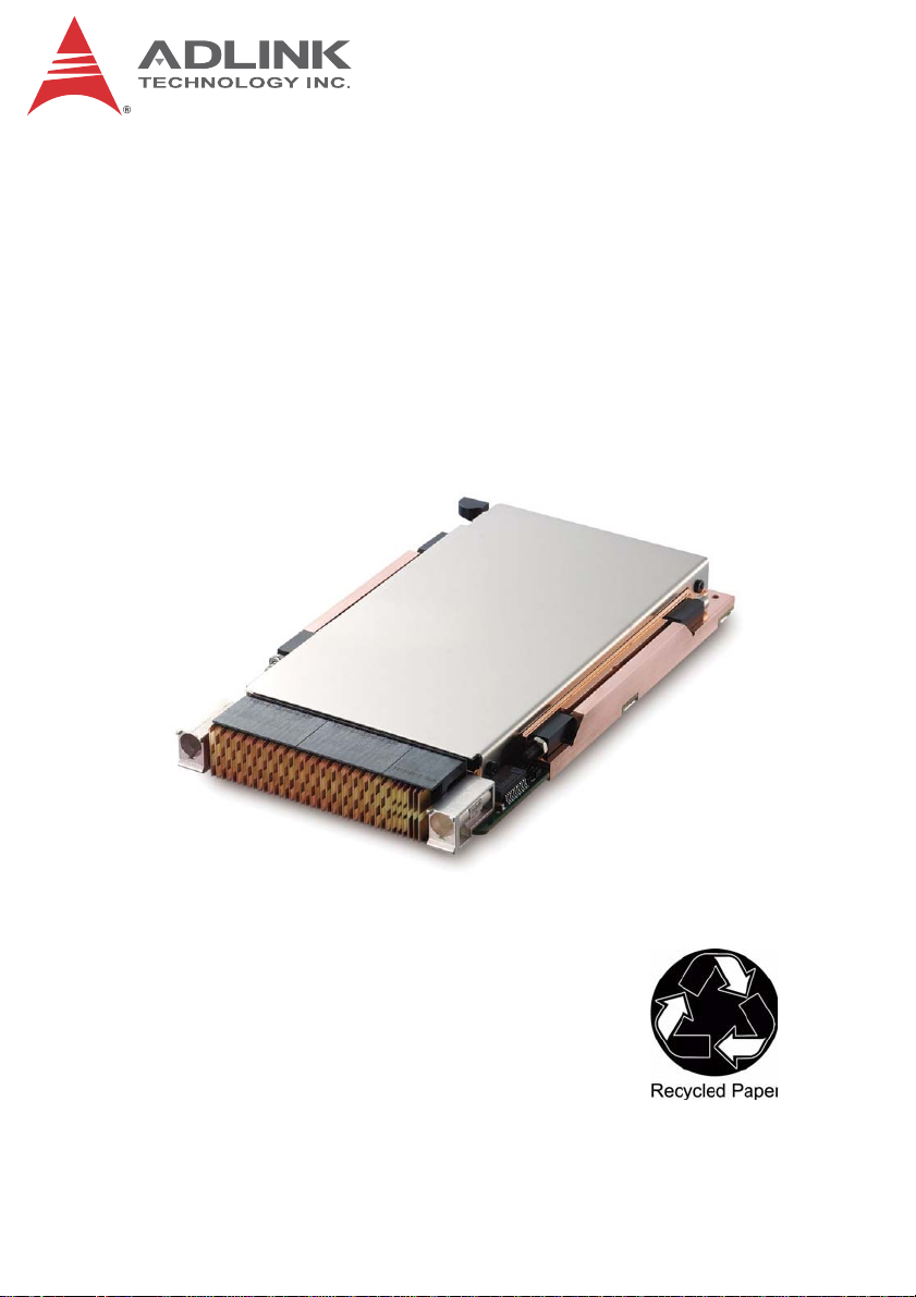
VPX3000 Series
Performance Rugged Conduction Cooled
3U VPX 3rd Gen Intel® Core™ i7
Processor Blade
Manual Rev.: 1.00
Revision Date: March 29, 2013
Part No: 50-15092-1000
Advance Technologies; Automate the World.
Page 2

Revision History
Revision Release Date Description of Change(s)
1.00 2013/03/29 Preliminary release
Page 3

VPX3000
Preface
Copyright 2013 ADLINK Technology Inc.
This document contains proprietary infor mation protected by copyright. All rights are reserved. No part of this manual may be reproduced by any mechanical, electronic, or other means in any form
without prior written permission of the manufacturer.
Disclaimer
The information in this document is subject to change without prior
notice in order to improve reliability, design, and function and does
not represent a commitment on the part of the manufa cturer.
In no event will the manufacturer be liable for direct, indirect, special, incidental, or consequential damages arising out of the use or
inability to use the product or documentation, even if advised of
the possibility of such damages.
Environmental Responsibility
ADLINK is committed to fulfill its social responsibility to global
environmental preservation through compliance with the European Union's Restriction of Hazardous Substances (RoHS) directive and Waste Electrical and Electronic Equipment (WEEE)
directive. Environmental protection is a top priority for ADLINK.
We have enforced measures to ensure that our products, manufacturing processes, components, and raw materials have as little
impact on the environment as possible. When products are at their
end of life, our customers are encouraged to dispose of them in
accordance with the product disposal and/or recovery programs
prescribed by their nation or company.
Trademarks
Product names mentioned herein are used for identification purposes only and may be trademarks and/or registered trademarks
of their respective companies.
Preface iii
Page 4

Using this Manual
Audience and Scope
The VPX3000 User’s Manual is intended for hardware technicians
and systems operators with knowledge of installing, configuring
and operating industrial grade computer systems.
Manual Organization
This manual is organized as follows:
Chapter 1, Introduction: Introduces the VPX3000, its features,
block diagrams, and package contents.
Chapter 2, Specifications: Presents detailed specification infor-
mation.
Chapter 3, Functional Description: Describes the VPX3000
main functions.
Chapter 4, Board Interfaces: Describes the VPX3000 and
VPX-R300 board interfaces.
Important Safety Instructions: Presents safety instructions all
users must follow for the proper setup, installation and usage of
equipment and/or software.
Getting Service: Contact information for ADLINK’s worldwide
offices.
iv Preface
Page 5
VPX3000
Conventions
Take note of the following conventions used throughout this
manual to make sure that users perform certain tasks and
instructions properly.
Additional information, aids, and tips that help users perform
tasks.
NOTE:
NOTE:
Information to prevent minor physical injury, component damage, data loss, and/or program corruption when trying to com-
CAUTION:
WARNING:
plete a task.
Information to prevent serious physical injury, component
damage, data loss, and/or program corruption when trying to
complete a specific task.
Preface v
Page 6

This page intentionally left blank.
vi Preface
Page 7

VPX3000
Table of Contents
Revision History...................................................................... ii
Preface.................................................................................... iii
List of Figures........................................................................ ix
List of Tables.......................................................................... xi
1 Introduction ........................................................................ 1
1.1 Overview.............................................................................. 1
1.2 Features............................................................................... 2
1.3 Block Diagrams.................................................................... 3
1.4 Model Number Decoder - Processor Blade........................ 6
1.5 Package Contents ............................................................... 7
2 Specifications..................................................................... 9
2.1 VPX3000 Blade Specifications ............................................ 9
2.2 VPX-R300 RTM Specifications..................... ... .... ... ... ... .... . 11
2.3 Power Consumption ............................... ... ... ..................... 12
3 Functional Description .................................................... 13
3.1 Processors......................................................................... 13
3.2 Chipset............................................................................... 15
3.3 Intel® Turbo Boost Technology......................................... 16
3.4 Intel® Hyper Threading Technology.................................. 16
3.5 PMC/XMC Site................................................................... 17
3.6 Real Time Clock ................................................................ 17
4 Board Interfaces............................................................... 19
4.1 VPX3000 Board Layout ..................................................... 19
4.2 VPX3000 Mechanical Drawing.......................................... 20
4.3 VPX3000 Connector Pin Assignments .............................. 21
Table of Contents vii
Page 8

4.4 VPX-R300 RTM Board Layout........................................... 26
4.5 VPX-R300 RTM Connector Pin Assignments.................... 27
4.6 Switches............................................................................. 34
Important Safety Instructions............................................... 35
Getting Service...................................................................... 37
viii Table of Contents
Page 9

VPX3000
List of Figures
Figure 1-1: VPX3000 Functional Block Diagram................................ 3
Figure 1-2: VPX-R300 RTM Functional Block Diagram.....................4
Figure 1-3: tBP-VPX3000 Test Backplane Functional Block Diagram5
Figure 4-1: VPX3000 Board Layout................................................. 19
Figure 4-2: VPX3000 Mechanical Drawing ...................................... 20
Figure 4-3: VPX-R300 RTM Board Layout....................................... 26
List of Figures ix
Page 10

This page intentionally left blank.
xList of Figures
Page 11

VPX3000
List of Tables
Table 2-1: VPX3000 Blade Specifications........................................9
Table 2-2: VPX-R300 RTM Specifications......................................11
List of Tables xi
Page 12

This page intentionally left blank.
xii List of Tables
Page 13

1 Introduction
1.1 Overview
The VPX3000 Series is a 3U VPX processor blade featuring the
3rd Generation Intel® Core i7 processor with Mobile Intel® QM77
Express Chipset. The VPX3000 provides up to 8GB
DDR3-1066/1333 dual channel ECC memory soldered onboard,
one PCI Express x8 XMC.3 site with VITA 46.9 rear IO, and
onboard soldered 16GB SLC SATA solid state drive. Rear I/O via
P1 and P2 includes 1000BASE-T, HD Audio (Line-in, Line-out), 2x
SATA 6 Gb/s, 1x SATA 3 Gb/s, USB 3.0, USB 2.0, GPIO, VGA,
DVI, RS-232, and RS-422.
A VPX-R300 Rear Transition Module is available to access rear
I/O signals and a tBP-VPX3000 Test Backplane supporting three
payload slots is available for users to validate VPX3000 functionality.
The VPX3000 Series is rugged conduction cooled with conformal
coating, making it ideal for mission critical applications such as
military and aerospace platforms.
VPX3000
Introduction 1
Page 14

1.2 Features
X 3U VPX VITA 46, OpenVPX VITA 65, VPX REDI 48
X 4HP (0.8") rugged conduction cooled 3U VPX blade with
conformal coating
X Intel® 3rd generation Core™ i7-3612QE Processor (4
cores, 6M cache, 2.1 GHz, 35W TDP)
X Dual channel DDR3-1333/1666 SDRAM with ECC soldered
onboard, up to 8GB
X Intel® QM77 PCH
X Intel® HD Graphics 4000 with DX11, OpenGL 3.1 and OCL
1.1
X Onboard PCI Express x8 XMC site with VITA 46.9 rear I/O
X Onboard soldered SATA Solid State Drive, up to 32GB
X Data Plane: VITA 46.4 PCIe 2.0 x8, or 2x PCIe 2.0 x4 to P1
X Control Plane: VITA 46.6 2x 1000BASE-BX
X Rear I/O:
Z P1: 1000BASE-T, Line-in, Line-out, 2x SATA 6 Gb/s,
USB 3.0, USB 2.0, 3x GPIO
Z P2: VGA, DVI, RS232, RS422, SATA Gen2, 3x GPIO
X RAID 0/1/5/10 support
X uEFI BIOS 8MB flash
X Module Profile: MOD3-PAY-2F2U-16.2.3-3
X Slot Profile: SLT3-PAY-2F2U-14.2.3
2Introduction
Page 15
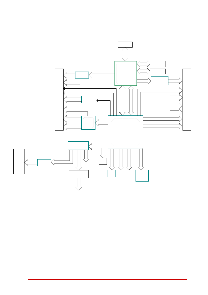
1.3 Block Diagrams
PCIe2.0x8 or PCIe2.0x4 + PCIe2.0x4
PCIe switch
PEX8619
GPIO 0,1,2*
SATA Gen3 Port 0,1
USB 3.0 Port 0 and USB 2.0 Port 0, 6
1000 BASE-T
ALC262
GbE
Intel
82580EB
Line-in, Line-out
P1
1000 BASE-BX
1000 BASE-BX
PCIE[8..15]
PCIe2.0x4
HDA
IMVP7
Vcore
Intel® Core™ i7
quad/dual-core
SV-BGA
DMI
FDI
Intel® QM77
PCH
PCIE[0..7]
PCIe2.0x8
A
B
On Board ECC
On Board ECC
XMC
VGA
DVI
SATA Gen2 Port 2
VPX3000
Max 512MBX8
Max 512MBX8
X8d+X12d
RS-422**
UART D**
GPIO 3**
P2
P0
IPMB
IPMC
A2F200M
UART C
F81216D
UART B
RS-232 to RS-422
**RS-422
**UART D
LPC
GPIO0~2*
SPI
Debug
Port
BIOS
GPIO3**
SATA Gen2 Port 3
On Board
Flash
Figure 1-1: VPX3000 Functional Block Diagram
Introduction 3
Page 16

RP0
VS1(DC12V), 8A/slot
VS2(DC3V), 8A/slot
VS3(DC5V), 16A/slot
DC3V_AUX,1A/Slot
DC12V_AUX,1A/Slot
DC-12V_AUX,1A/Slot
VBAT
NVMRO, SYSRESET#
RP1
RP2
SATA 0 ~ SATA 1
USB 2.0
USB3.0 +USB2.0
DVI signal
VGA signal
AC signal_LI
AC signal_LO
10/100/1000BASE-T
GPIO signal
SATA3.0
2 port
USB2.0
1 port
USB3.0
1 port
DVI-I
1 port
Audio jack(LI)
1 port
Audio jack(LO)
1 port
RS-232
1 port
RS-422
1 port
RJ-45 jack
GPIO
8 pin header
XMC P2 onboard
1 port
Figure 1-2: VPX-R300 RTM Functional Block Diagram
4Introduction
Page 17

VPX3000
2x PCIe by 4
1000BASE-T
Slot#2Slot#1
Crossover
Crossover
X
B-ESAB0001
x
e
2
ICP
1000BASE-T
4 yb
XB-ESAB0001
Slot#3
2
x
LAN
KVM I/O
XMC I/O
VS1(DC12V), 32A/slot
VS2(DC3V), 32A/slot
VS3(DC5V), 23A/slot
DC3V_AUX,1A/Slot
DC12V_AUX,1A/Slot
DC-12V_AUX,1A/Slot
REF_CLK+/-
SM[0:1] IPM2, SM[2:3] I2C
NVMRO, SYSRESET#, JTAG
VBAT
4 yb eICP
PCIE8~PCIE15
2x GbE 1000BASE-BX
10/100/1000BASE-T
SATA 0 ~ SATA 1
USB 2.0
USB3.0 +USB2.0
DVI signal
VGA signal
AC signal
GPIO signal
PCIE x4
2 Slots
4xSMA
RJ-45 jack
SATA3.0
2 port
USB2.0
1 port
USB3.0
1 port
DVI-I
1 port
Audio jack(LI/LO)
1 port
RS-232
1 port
RS-422
1 port
GPIO LED
4 port
XMC P2 onboard
1 port
Figure 1-3: tBP-VPX3000 Test Backplane Functional Block Diagram
Introduction 5
Page 18

1.4 Model Number Decoder - Processor Blade
VPX3000/3612/M8/S16-R1
(A) (B) (C) (D)
(A) CPU Code
Z 3612 = Quad-Core Intel® i7-3612QE processor
Z 3555 = Dual-Core Intel® i7-2655LE processor
(B) Memory Size Code
Z M8 = Onboard 8GB DDR3-1333/1600 memory
Z M16 = Onboard 16GB DDR3-1333/1600 memory
(C) SA TA NAND Flash Size Code
Z S16 = Onboard 16GB
Z S32 = Onboard 32GB
(D) Ruggedized Level Code
Z R1 = Conduction Cooled version with conformal coating
supporting -40°C to +75°C at card edge
Z R2 = Conduction Cooled version with conformal coating
supporting -40°C to +85°C at card edge
6Introduction
Page 19

VPX3000
1.5 Package Contents
The VPX3000 is packaged with the following components. If any
of the items on the contents list are missing or damaged, retain the
shipping carton and packing material and contact the dealer for
inspection. Please obtain authorization before returning any product to ADLINK. The packing contents of the VPX3000 are
non-standard configurations and may vary depending on customer
requests.
Processor Blade
X VPX3000
Z CPU and memory specifications will differ depending on
options selected
Z Thermal module is assembled on the board
X ADLINK Driver USB Flash Drive
Rear Transition Module
X VPX-R300 RTM
X DVI to VGA adapter
Test Backplane
X tBP-VPX3000 test backplane
X DVI to VGA adapter
The contents of non-standard VPX3000 configurations may
vary depending on the customer requirements.
NOTE:
NOTE:
This product must be protected from static discharge and physical shock. Never remove any of the components except at a
CAUTION:
Introduction 7
static-free workstation. Use the anti-static bag shipped with the
product when putting the board on a surface. Wear an
anti-static wrist strap properly grounded on one of the system's
ESD ground jacks when installing or servicing system components.
Page 20

This page intentionally left blank.
8Introduction
Page 21

VPX3000
2 Specifications
2.1 VPX3000 Blade Specifications
VITA Standards • VITA 46.0 VPX Base Standard
• VITA 46.4 PCI Express on VPX Fabric Connector
• VITA 46.6 Gigabit Ethernet Control Plane on VPX
• VITA 46.9 PMC/XMC/Ethernet Signal Mapping to 3U/6U
VPX
• VITA 46.11(draft) System Management on VPX
• VITA 48.0 Ruggedized Enhanced Design Implementation
Mechanical Base Specification
• VITA 65 OpenVPX Architecture Framework for VPX
Mechanical • IEEE 1101.1-1998 - Mechanical Core Specifications for
Microcomputers
• IEEE 1101.2-1992 - Conduction Cooled VME Mechanics
•3U 4HP (0.8")
• Board size: 100mm x 160mm
• P0, P1, P2 connectors; alignment key 1 & 2 equipped
Processor • Intel® Core™ i7-3612QE Processor, 2.1 GHz, 6MB LLC
cache, FCBGA1023, TDP 35W
• Intel® Core™ i7-3555LE Processor, 2.5 GHz, 4MB LLC
cache, FCBGA1023, TDP 25W
• Passive ruggedized heatsink
Chipset • Intel® BD82QM77 Platform Controller Hub (PCH)
Memory • Dual channel DDR3-1333/1600 ECC memory
• Soldered onboard with 256Mb*8*18 devices
•Up to 8GB
PCI Express • PCI Express 2.0 x8, or 2x PCIe x4 to P1 by switch setting
Gigabit
Ethernet
Graphics • Integrated in Intel® Core™ i7 processor
• One Intel® 82580EB Gigabit Ethernet Controller
• One 10/100/1000BASE-T port and two 1000BASE-BX
SerDes ports to P1
• Intel HD Graphics 4000
• Analog VGA and digital DVI routed to P2
• DVI port resolutions up to 1920x1200 at 60Hz
• Analog monitor support up to 2048x1536 at 75Hz
• Dual independent display
T a ble 2-1: VPX3000 Blade S p ecificat ions
Specifications 9
Page 22

XMC • One PCIe 2.0 x8 conduction cooled XMC.3 site
• Jn6 rear XMC I/O connector compliant to VITA 46.9,
X8d+X12d
Front Panel I/O • Reset button
• Power LED
Storage
Interfaces
• Onboard SATA NAND flash on SATA 3 Gb/s, up to 32GB
1
• SATA 6 Gb/s port 0 and 1 to P1
• SATA 3 Gb/s port 2 to P2
BIOS • AMI EFI BIOS, 64Mbit SPI flash memory
P1 Interface • Line-in
• Line-out
• 2x SATA 6 Gb/s ports
• 2x USB 2.0
• USB 3.0
• 10/100/1000BASE-T Gigabit Ethernet Ports
• 2x 1000BASE-BX SerDes Port
P2 Interface •VGA
•RS-232
•RS-422
•DVI
• SATA 3 Gb/s port
• XMC X8d+X12d
Environmental • Operating Temperature:
-40°C to +75°C (for Intel® Core™ i7-3612QE)
-40°C to +85°C (for Intel® Core™ i7-3555LE)
• Storage Temperature: -50°C to 100°C
• Humidity: 95%, non-condensing
• Shock: 40G peak-to-peak, 11ms duration, non-operating
•Vibration
1
: Operating 5Grms, 20-2000Hz, each axis w/o
hard drive
• Altitude:
EMI • CE EN55022
• FCC Class A
Table 2-1: VPX3000 Blade Specifications
Notes:
1. The storage device limits the operational vibration. When application requires higher specification for anti-vibration, it is recommended to use a flash storage device.
10 Specifications
Page 23

2.2 VPX-R300 RTM Specifications
VITA Standards • VITA 46.10 Rear Transition Module on VPX
Mechanical • 100mm x 80mm
Faceplate I/O • DVI-I port
• USB 2.0 port
• USB 3.0 port
• 10/100/1000BASE-T Ethernet port
Onboard
Interfaces
Note: Specifications are subject to change without prior notice.
• Line-in audio jack
• Line-out audio jack
• RS-232 (RJ-45)
• RS-422 (RJ-45)
• 2x SATA 3.0 ports
• 8x pin headers for GPIO
•XMC port
• 4x status LEDs for GPIO
Table 2-2: VPX-R300 RTM Specifications
VPX3000
Specifications 11
Page 24

2.3 Power Consumption
TBD
12 Specifications
Page 25

3 Functional Description
The following sections describe the VPX3000 features and
functions.
3.1 Processors
The 3rd Generation Intel® Core™ i7 Processo r is the next gener ation of 64-bit, multi-core mobile processors built on 22-nanometer
process technology. Based on a new micro-architecture, the processor is designed for a two-chip platform. The two-chip platform
consists of a processor and Platform Controller Hub (PCH). The
platform enables higher performance, lower cost, easier validation, and improved x-y footprint. The processor includes an integrated display engine, processor graphics, integrated memory
controller, and integrated I/O on a single silicon die.
Features Core™ i7-3612QE Core™ i7 -3555LE
Clock 2.1 GHz 2.5 GHz
Max. Single Core Turbo
Freq.
Last Level Cache 6 MB 4 MB
No. of Cores/Threads 4/8 2/4
1
Maximum Power (TDP
T
junction,MAX
2
)
3.1 GHz 3.2 GHz
35 W 25 W
105°C 105°C
VPX3000
Notes:
1. The highest expected sustainable power wh ile running known
power intensive applications. TDP is not the maximum power
that the processor can dissipate.
2. The maximum supported operating temperature.
Functional Description 13
Page 26

Supported Technologies
Z Intel® Virtualization Techno logy for Directed I/O (Intel®
VT-d)
X Intel® Virtualization Technology (Intel® VT-x)
X Intel® vPro Technology (Intel® VT)
X Intel® Trusted Execution Technology (Intel® TXT)
X Intel® Hyper-Threading Technology
X Intel® 64 Architecture
X Intel® Turbo Boost Technology 2.0
X AES New Instructions
X Intel® My WiFi Technology
X Enhanced Intel SpeedStep® Technology
X Thermal Monitoring Technologies
X Intel® Fast Memory Access
X Execute Disable Bit
X Intel® VT-x with Extended Page Tables (EPT)
Interfaces
X Dual channel DDR3 memory with one channel of unbuffered
SODIMM and one channel of soldered SDRAM
X Memory DDR3 data transfer rates of 1333 MT/s and 1600
MT/s
X 64-bit wide channels plus 8-bits of ECC support for each
channel
X System Memory Interface I/O Vo ltage of 1.35V and 1.5V
X 1-Gb, 2-Gb, and 4-Gb DDR3 DRAM technologies supported
Z Using 4Gb DRAM device technologies, the largest mem-
ory capacity possible is 8 GB.
Z Intel Fast Memory Access:
Just-in-Time Command Scheduling
Command Overlap
Out-of Order Scheduling
X The PCI Express lanes are fully-compliant with the PCI
Express Base Specification, Revision 3.0, including support
for 8.0 GT/s transfer speeds.
14 Functional Description
Page 27

VPX3000
3.2 Chipset
The VPX3000 incorporates the Mobile Intel® QM77 Express Chipset (Intel® BD82QM77 PCH).
Mobile Intel® QM77 Express Chipset
X PCI Express Base Specification, Revision 2.0 support for up
to eight ports with transfer rate up to 5 GT/s
X Supports dual display
X ACPI Power Management Logic Support, Revision 4.0a
X Enhanced DMA controller, interrupt controller, and timer
functions
X Integrated Serial ATA host controllers with independent
DMA operation on up to six ports and SATA 6.0 Gb/s up to
two ports
X Supports USB 2.0, USB 3.0
X USB host interface with two EHCI high-speed USB 2.0 Host
controllers and two rate matching hubs provide support for
up to fourteen USB 2.0 ports
X System Management Bus (SMBus) Specification, Version
2.0 with additional support for I2C devices
X Supports Intel Trusted Execution Technology
X Support vPro Technology
X Supports Intel® High Definition Audio
X Supports Intel® Rapid Storage Technology
X Supports Intel® Virtualization Technology for Directed I/O
X Low Pin Count (LPC) interface
X Serial Peripheral Interface (SPI) support
Functional Description 15
Page 28

3.3 Intel® Turbo Boost Technology
Intel Turbo Boost Technology is a feature that allows the processor
to opportunistically and automatically run faster than its rated
operating core and/or render clock frequency when there is sufficient power headroom, and the product is within specified temperature and current limits. The Intel Turbo Boost Technology feature
is designed to increase performance of both multi-threaded and
single-threaded workloads. The processor supports a Turbo mode
where the processor can use the thermal capacity associated with
package and run at power levels higher than TDP power for short
durations. This improves the system responsiveness for short,
bursty usage conditions.
Turbo Mode availability is independent of the number of active
cores; however, the Turbo Mode frequency is dynamic and dependent on the instantaneous application power load, the number of
active cores, user configurable settings, operating environment,
and system design. If the power, current, or thermal limit is
reached, the processor will automatically reduce the frequency to
stay with its TDP limit.
3.4 Intel® Hyper Threading Technology
The processor supports Intel® Hyper-Threading Technology
(Intel® HT Technology), that allows an execution core to function
as two logical processors. While some execution resources (such
as caches, execution units, and buses) are shared, each logical
processor has its own architectural state with its own set of general-purpose registers and control registers. This feature must be
enabled using the BIOS and requires operating system support.
16 Functional Description
Page 29

VPX3000
3.5 PMC/XMC Site
The VPX3000 Series supports one XMC site for rear I/O expansion. The XMC site provides a x8 PCI Express 2.0 lane. Jn6 rear
XMC I/O connector is compliant to VITA 46.9, X8d+X12d.
3.6 Real Time Clock
The Intel® QM77 PCH contains a Motorola MC146818B-compatible real-time clock (RTC) with 256 bytes of RAM. The real-time
clock performs two key functions: keeping track of the time of day
and storing system data. The RTC operates on a 32.768 KHz
crystal and is powered by P3V3_AUX or VBAT. There is no external RTC battery on the VPX3000 to power the RTC after the system is powered off.
Functional Description 17
Page 30

This page intentionally left blank.
18 Functional Description
Page 31

4 Board Interfaces
X
VPX3000
4.1 VPX3000 Board Layout
(1.6)
(160)
MC
SW
LAN
SSD
P0
P1
P2
BRG
RAM
(99.85)
CPU
PCH
Jn6
CPU Intel Core Processor SSD 16/32GB SATA NAND
Flash
PCH Intel QM77 PCH J15 XMC Connector
BRG Pericom PEX8619
Bridge
LAN Intel 82580EB
Ethernet Controller
Jn6 XMC Rear I/O
Connector
SW DIP Switch for PCIe to
P1 configuration
RAM DDR3 Memory Chips P0-2 VPX Connectors
Figure 4-1: VPX3000 Board Layout
Board Interfaces 19
Page 32

Power LED
4.2 VPX3000 Mechanical Drawing
160
99.85
14.34 4.6
18.94
Figure 4-2: VPX3000 Mechanical Drawing
Power LED
LED Color Condition Indication
Power
Green
20 Board Interfaces
OFF System is off
ON System is on
Page 33

4.3 VPX3000 Connector Pin Assignments
XMC Connectors
F1 F19
VPX3000
A1
A19
JN1 Connector
Pin A B C D E F
1
RXP0 RXN0 +3.3V RXP1 RXN1 VPWR
2
GND GND TRST# GND GND MRSTI#
3
RXP2 RXN2 +3.3V RXP3 RXN3 VPWR
4
GND GND TCK GND GND MRSTO#
5
RXP4 RXN4 +3.3V RXP5 RXN5 VPWR
6
GND GND TMS GND GND +12V
7
RXP6 RXN6 +3.3V RXP7 RXN7 VPWR
8
GND GND TDI GND GND -12V_AUX
9
10
11
12
13
14
15
16
17
18
19
NC NC NC NC NC NC
GND GND TDO GND GND GA0
TXP0 TXN0 MBIST# TXP1 TXN1 VPWR
GND GND GA1 GND GND MPRSENT#
TXP2 TXN2 +3.3V_AUX TXP3 TXN3 VPWR
GND GND GA2 GND GND DATA
TXP4 TXN4 NC TXP5 TXN5 VPWR
GND GND MVMRO GND GND CLK
TXP6 TXN6 NC TXP7 TXN7 NC
GND GND NC GND GND NC
CLK-P CLK-N NC WAKE# ROOT# NC
Board Interfaces 21
Page 34

JN2 Connector
Pin A B C D E F
1
JN6_A1 JN6_B1 NC JN6_D1 JN6_E1 NC
2
3
4
5
6
7
8
9
10
11
12
13
14
15
16
17
18
19
GND GND NC GND GND NC
JN6_A3 JN6_B3 NC JN6_D3 JN6_E3 NC
GND GND NC GND GND NC
JN6_A5 JN6_B5 NC JN6_D5 JN6_D6 NC
GND GND NC GND GND NC
JN6_A7 JN6_B7 NC JN6_D7 JN6_D7 NC
GND GND NC GND GND NC
JN6_A9 JN6_B9 NC JN6_D9 JN6_D9 NC
GND GND NC GND GND NC
JN6_A11 JN6_B11 NC JN6_D1 1 JN6_D11 NC
GND GND NC GND GND NC
JN6_A13 JN6_B13 NC JN6_D13 JN6_D13 NC
GND GND NC GND GND NC
JN6_A15 JN6_B15 NC JN6_D15 JN6_D16 NC
GND GND NC GND GND NC
JN6_A17 JN6_B17 NC JN6_D17 JN6_D17 NC
GND GND NC GND GND NC
JN6_A19 JN6_B19 NC JN6_D19 JN6_D19 NC
22 Board Interfaces
Page 35

VPX3000
VPX Connectors
P0 Connector
Pin G F E D C B A
1 +12V +12V +12V None +3.3V +3.3V +3.3V
2 +12V +12V +12V None +3.3V +3.3V +3.3V
3 +5V +5V +5V None +5V +5V +5V
4 I2C_CLK I2C_DAT GND +12V_AUX GND SYSRESET NC
5 GAP GA4 GND +3.3V_AUX GND SM0_CLK SM1_DATA
6 GA3 GA2 GND +12V_AUX GND GA1 GA0
7 TCK GND TDO TDI GND TMS TRST
8 GND REF_CLK- REF_CLK+ GND NC NC GND
Board Interfaces 23
Page 36

P1 Connector
Pin G F E D C B A
1NC GND L0-TX- L0-TX+ GND L0-RX- L0-RX+
2GND
3 VBAT GND
4GND
5 SYSCON# GND
6GND
7NC GND
8GND
9 GPIO1 GND
10 GND
11 GPIO6 GND
12 GND
13 GPIO7 GND
14 GND
MASKABLE
15
_RESET
16 GND
L1-TX- L1-TX+ GND L1-RX- L1-RX+ GND
L2-TX- L2-TX+ GND L2-RX- L2-RX+
L3-TX- L3-TX+ GND L3-RX- L3-RX+ GND
L4-TX- L4-TX+ GND L4-RX- L4-RX+
L5-TX- L5-TX+ GND L5-RX- L5-RX+ GND
L6-TX- L6-TX+ GND L6-RX- L6-RX+
L7-TX- L7-TX+ GND L7-RX- L7-RX+ GND
SATA0-TX- SATA0-TX+ GND SATA0-RX- SATA0-RX+
SATA1-TX- SATA1-TX+ GND SATA1-RX- SATA1-RX+ GND
USB3_RX1- USB3_RX1+ GND USB3_TX1- USB3_TX1+
USB2_0- USB2_0+ GND USB2_6- USB2_6+ GND
TP01_DB- TP01_DB+ GND TP01_DA- TP01_DA+
TP01_DD- TP01_DD+ GND TP01_DC- TP01_DC+ GND
GND
UTP1_TD- UTP1_TD+ GND UTP1_RD- UTP1_RD+ GND
UTP2_TD- UTP2_TD+ GND UTP2_RD- UTP2_RD+
Lxx: PCI Express x8
SATAxx : SATA
USB3xx: USB 3.0
USB2xx: USB 2.0
TPxx: 1000 BASE-T
UTPxx: 1000 BASE-BX
24 Board Interfaces
Page 37

VPX3000
P2 Connector
Pin G F E D C B A
1GPIO3 GND DVI_TX1- DVI_TX1+ GND DVI_TX0- DVI_TX0+
2GND
VGA_SDA GND NC DVI_HPD GND DVI_SCL DVI_SDA
3
4GND
VGA_SCL GND RS422_TX- RS422_TX+ GND RS422_RX- RS422_RX+
5
6GND
VGA-HS GND J16-A1 J16-B1 GND J16-D1 J16-E1
7
8GND
VGA-VS GND J16-A11 J16-B11 GND J16-D11 J16-E11
9
10 GND
VGA-R GND J16-A5 J16-B5 GND J16-D5 J16-E5
11
12 GND
VGA-B GND J16-A9 J16-B9 GND J16-D9 J16-E9
13
14 GND
VGA-G GND J16-A17 J16-B17 GND J16-D17 J16- E17
15
16 GND
DVI_TXC- DVI_TXC+ GND DVI_TX2- DVI_TX2+ GND
COM_SIN COM_SOUT GND COM_CTS# COM_RTS# GND
Linein-L Linein-R AGND Lineout-L Lineout-R AGND
J16-A3 J16-B3 GND J16-D3 J16-E3 GND
J16-A13 J16-B13 GND J16-D13 J16-E13 GND
J16-A7 J16-B7 GND J16-D7 J16-E7 GND
J16-A15 J16-B15 GND J16-D15 J16-E15 GND
J16-A19 J16-B19 GND J16-D19 J16-E19 GND
DVIxx : DVI
COMxx: RS-232
RS422xx: RS-422
Linexx: Audio
VGAxx: Analog VGA
Jxx: XMC rear I/O (Jn6)
Board Interfaces 25
Page 38

4.4 VPX-R300 RTM Board Layout
(83.5)
AP1
CN11 CN12
CN1
(99.85)
CN2
CN3
AP2
CN9
CN13
CN10
CN4
CN5
CN8
CN7
CN15
CN6
(20)
CN1 VPX Connector RP0 CN8 DVI-I port
CN2 VPX Connector RP1 CN9 Line-in Port
CN3 VPX Connector RP2 CN10 Line-out Port
AP1/2 Alignment keys CN11 RS-232 Port
CN4/5 7-pin SATA connectors CN12 RS-422 Port
CN6 USB 3.0 port CN13 XMC connector
CN7 USB 2.0 port CN15 1000BASE-T port
Figure 4-3: VPX-R300 RTM Board Layout
26 Board Interfaces
Page 39

4.5 VPX-R300 RTM Connector Pin Assignments
Rear I/O Connectors
Gigabit Ethernet Connectors (CN1 1, RJ-45 )
Pin # GbE Signal
1MX0+
2MX03MX1+
4MX2+
5MX26MX17MX3+
8MX3-
USB 2.0 Connector (CN1 6)
Pin # Signal Name
1+5V
2 USB3 USB+
4GND
18
VPX3000
Board Interfaces 27
Page 40

USB 3.0 Connector (CN15)
Pin # Signal Name
1+5V
2 Data3 Data+
4GND
5RX_N
6RX_P
7GND
8TX_N
9TX_P
DVI-I Connector (CNY1-R)
Pin # Signal Pin # Signal
1NC16NC
2NC17NC
3 GND 18 NC
4NC19GND
5NC20NC
6 DDCCLK_5V 21 NC
7 DDCDAT_5V 22 GND
8 VSYNC 23 NC
9NC24NC
10 NC C1 RED
11 GND C2 GREEN
12 NC C3 BLUE
13 NC C4 HSYNC
14 P5V C5 GND
15 GND
28 Board Interfaces
Page 41

Onboard Connectors
SATA Connector (CN12/13)
VPX3000
Pin # Signal
1GND
2TXP
3TXN
4GND
5RXN
6RXP
7GND
RS-232 (CN31, RJ-45)
Pin # RS-232
1N.C.
2 S3_RTS-L(RTS)
3N.C.
4 S3_SOUT(TXD)
5 S3_SIN(RXD)
6 GND.
7 S3_CTS-L(CTS)
8N.C.
RS-422 (CN32, RJ-45)
1
2
3
4
5
6
7
18
Pin # RS-232
1 S3_TXD4222N.C.
3N.C.
4 S3_RXD422+
5 S3_TXD422+
18
6GND
7N.C.
8 S3_RXD422-
Board Interfaces 29
Page 42

XMC Connector (CN36)
F1 F19
A1
A19
Pin A B C D E F
1 +5V S3_JN6-E1 S3_JN6-D1 +3.3V S3_JN6-B1 S3_JN6-A1
2 NC GND GND TRST# GND GND
3 +5V S3_JN6-E3 S3_JN6-D3 +3.3V S3_JN6-B3 S3_JN6-A3
4 NC GND GND TCK GND GND
5 +5V S3_JN6-E5 S3_JN6-D5 +3.3V S3_JN6-B5 S3_JN6-A5
6 +12V GND GND TMS GND GND
7 +5V S3_JN6-E7 S3_JN6-D7 +3.3V S3_JN6-B7 S3_JN6-A7
8 -12V GND GND TDI GND GND
9 +5V S3_JN6-E9 S3_JN6-D9 +3.3V S3_JN6-B9 S3_JN6-A9
10 GA0 GND GND TDO GND GND
11 +5V S3_JN6-E11 S3_JN6-D11 NC S3_JN6-B11 S3_JN6-A11
12 GND GND GND GA1 GND GND
13 +5V S3_JN6-E13 S3_JN6-D13 3.3V_AUX S3_JN6-B13 S3_JN6-A13
14 XMC_DAT GND GND GA2 GND GND
15 +5V S3_JN6-E15 S3_JN6-D15 NC S3_JN6-B15 S3_JN6-A15
16 XMC_CLK GND GND NVMRO GND GND
17 NC S3_JN6-E17 S3_JN6-D17 NC S3_JN6-B17 S3_JN6-A17
18 NC GND GND NC GND GND
19 NC S3_JN6-E19 S3_JN6-D19 NC S3_JN6-B19 S3_JN6-A19
30 Board Interfaces
Page 43

VPX3000
RTM VPX Connectors
RP0 Connector
Pin G F E D C B A
1 +12V +12V +12V +12V NC +3.3V +3.3V
2 +12V +12V +12V +12V NC +3.3V +3.3V
3 +5V +5V +5V +5V NC +5V +5V
4 SM2 SM3 GND -12V_AUX GND SYSRESET NVMRO
5 GAP* GA4* GND 3.3V_AUX GND SM0 SM1
6 GA3* GA2* GND +12V_AUX GND GA1* GA0*
7 TCK GND TDO TDI GND TMS TRST*
8 GND REF_CLK- REF_CLK+ GND RES_BUS- RES_BUS+ GND
9 NC GND NC NC GND NC NC
10 GND NC NC GND NC NC GND
11 P1_VBAT GND NC NC GND NC NC
12 GND NC NC GND NC NC GND
13 SYSCON# GND NC NC GND NC NC
14 GND NC NC GND NC NC GND
15 ? GND NC NC GND NC NC
16 GND NC NC GND NC NC GND
Board Interfaces 31
Page 44

RP1 Connector
Pin G F E D C B A
1 GPIO0 GND NC NC GND NC NC
2 GND NC NC GND NC NC GND
3 GPIO1 GND NC NC GND NC NC
4 GND NC NC GND NC NC GND
5 GPIO2 GND MDIN1 MDIP1 GND MDIN0 MDIP0
6 GND MDIN3 MDIP3 GND MDIN2 MDIP2 GND
7 Maskreset GND NC NC GND NC NC
8 GND NC NC GND NC NC GND
9 GPIO3 GND DVI_TX1- DVI_TX1+ GND DVI_TX0- DVI_TX0+
10 GND DVI_TXC- DVI_TXC+ GND DVI_TX2- DVI_TX2+ GND
11 VGA_SDA GND ? DVI_HPD GND DVI_SCL DVI_SDA
12 GND SIN SOUT GND CTS# RTS# GND
13 VGA_SCL GND RS422_TX- RS422_TX+ GND RS422_RX- RS422_RX+
14 GND Linein-L Linein-R AGND Lineout-L Lineout-R AGND
15 VGA-HS GND J16-A1 J16-B1 GND J16-D1 J16-E1
16 GND J16-A3 J16-B3 GND J16-D3 J16-E3 GND
32 Board Interfaces
Page 45

VPX3000
RP2 Connector
Pin G F E D C B A
1 VGA-VS GND J16-A11 J16-B11 GND J16-D11 J16-E11
2 GND J16-A13 J16-B13 GND J16-D13 J16-E13 GND
3 VGA-R GND J 16-A5 J16-B5 GND J16-D5 J16-E5
4 GND J16-A7 J16-B7 GND J16-D7 J16-E7 GND
5 VGA-B GND J16-A9 J16-B9 GND J16-D9 J16-E9
6 GND J16-A15 J16-B15 GND J16-D15 J16-E15 GND
7 VGA-G GND J16-A17 J16-B17 GND J16-D17 J16-E17
8 GND J16-A19 J16-B19 GND J16-D19 J16-E19 GND
Board Interfaces 33
Page 46

4.6 Switches
PCI Express to P1 Configuration Switch (SW)
This switch sets the PCI Express Lane configur ation at the P1
connector.
Mode 1 2 3 4
8x PCIe x1 OFF ON OFF ON
1x PCIe x4 + 4x PCIe x1
2x PCIe x4 (default)
PCIe x8 ON OFF OFF OFF
OFF ON ON OFF
OFFONONON
34 Board Interfaces
Page 47

VPX3000
Important Safety Instructions
For user safety, please read and follow all instructions,
WARNINGS, CAUTIONS, and NOTES marked in this manual
and on the associated equipment before handling/operating the
equipment.
X Read these safety instructions carefully.
X Keep this user’s manual for future reference.
X Read the specifications section of this manual for detailed
information on the operating environment of this equipment.
X When installing/mounting or uninstalling/removing
equipment:
Z Turn off power and u nplug any power cords/cables.
X To avoid electrical shock and/or damage to equipment:
Z Keep equipment away from water or liquid sources;
Z Keep equipment away from high heat or high humidity;
Z Keep equipment properly ventilated (do not block or
cover ventilation openings);
Z Make sure to use recommended voltage and powe r
source settings;
Z Always install and operate equipment near an easily
accessible electrical socket-outlet;
Z Secure the power cord (do not place any obje ct on /ove r
the power cord);
Z Only install/attach and operate equipment on stable
surfaces and/or recommended mountings; and,
Z If the equipment will not be used for long periods of time,
turn off and unplug the equipment from its power source.
Important Safety Instructions 35
Page 48

X Never attempt to fix the equipment. Equipmen t sho u ld on ly
be serviced by qualified personnel.
A Lithium-type battery may be provided for uninterrupted, backup
or emergency power.
Risk of explosion if battery is replaced with one of an incorrect
WARNING:
type. Dispose of used batteries appropriately.
X Equipment must be serviced by authorized technicians
when:
Z The power cord or plug is damaged;
Z Liquid has penetrated the equipment;
Z It has been exposed to high humidity/moisture;
Z It is not functioning or does not function according to the
user’s manual;
Z It has been dropped and/or damaged; and/or,
Z It has an obvious sign of breakage.
36 Important Safety Instructions
Page 49

Getting Service
Contact us should you require any service or assistance.
ADLINK Technology, Inc.
Address: 9F, No.166 Jian Yi Road, Zhonghe District
New Taipei City 235, Taiwan
ᄅקؑխࡉ৬ԫሁ 166 ᇆ 9 ᑔ
Tel: +886-2-8226-5877
Fax: +886-2-8226-5717
Email: service@adlinktech.com
Ampro ADLINK Technology, Inc.
Address: 5215 Hellyer Avenue, #110, San Jose, CA 95138, USA
Tel: +1-408-360-0200
Toll Free: +1-800-966-5200 (USA only)
Fax: +1-408-360-0222
Email: info@adlinktech.com
ADLINK Technology (China) Co., Ltd.
Address: Ϟ⍋Ꮦ⌺ϰᮄᓴ∳催⾥ᡔು㢇䏃 300 ো(201203)
300 Fang Chun Rd., Zhangjiang Hi-Tech Park,
Pudong New Area, Shanghai, 201203 China
Tel: +86-21-5132-8988
Fax: +86-21-5132-3588
Email: market@adlinktech.com
VPX3000
ADLINK Technology Beijing
Address: ࣫ҀᏖ⍋⎔Ϟഄϰ䏃 1 োⲜ߯ࡼ E ᑻ 801 ᅸ(100085)
Tel: +86-10-5885-8666
Fax: +86-10-5885-8626
Email: market@adlinktech.com
ADLINK Technology Shenzhen
Address: ⏅ഇᏖቅ⾥ᡔು催ᮄϗ䘧᭄ᄫᡔᴃು
Tel: +86-755-2643-4858
Fax: +86-755-2664-6353
Email: market@adlinktech.com
LiPPERT ADLINK Technology GmbH
Address: Hans-Thoma-Strasse 11, D-68163, Mannheim, Germany
Tel: +49-621-43214-0
Fax: +49-621 43214-30
Email: emea@adlinktech.com
Rm. 801, Power Creative E, No. 1, B/D
Shang Di East Rd., Beijing, 100085 China
A1 2 ὐ C (518057)
2F, C Block, Bldg. A1, Cyber-Tech Zone, Gao Xin Ave. Sec. 7,
High-Tech Industrial Park S., Shenzhen, 518054 China
Getting Service 37
Page 50

ADLINK Technology, Inc. (French Liaison Office)
Address: 15 rue Emile Baudot, 91300 Massy CEDEX, France
Tel: +33 (0) 1 60 12 35 66
Fax: +33 (0) 1 60 12 35 66
Email: france@adlinktech.com
ADLINK Technology Japan Corporation
Address: ͱ101-0045 ᵅҀ䛑ҷ⬄⼲⬄䤯ފ⬎ 3-7-4
Tel: +81-3-4455-3722
Fax: +81-3-5209-6013
Email: japan@adlinktech.com
ADLINK Technology, Inc. (Korean Liaison Office)
Address: 昢殾柢 昢爎割 昢爎壟 1675-12 微汾瘶捒娯 8猻
Tel: +82-2-2057-0565
Fax: +82-2-2057-0563
Email: korea@adlinktech.com
ADLINK Technology Singapore Pte. Ltd.
Address: 84 Genting Lane #07-02A, Cityneon Design Centre,
Tel: +65-6844-2261
Fax: +65-6844-2263
Email: singapore@adlinktech.com
ADLINK Technology Singapore Pte. Ltd. (Indian Liaison Office)
Address: 1st Floor, #50-56 (Between 16th/17th Cross) Margosa Plaza,
Tel: +91-80-65605817, +91-80-42246107
Fax: +91-80-23464606
Email: india@adlinktech.com
⼲⬄ 374 ɛɳ 4F
KANDA374 Bldg. 4F, 3-7-4 Kanda Kajicho,
Chiyoda-ku, Tokyo 101-0045, Japan
8F Mointer B/D,1675-12, Seocho-Dong, Seocho-Gu,
Seoul 137-070, Korea
Singapore 349584
Margosa Main Road, Malleswaram, Bangalore-560055, India
ADLINK Technology, Inc. (Israeli Liaison Office)
Address: 6 Hasadna St., Kfar Saba 44424, Israel
Tel: +972-9-7446541
Fax: +972-9-7446542
Email: israel@adlinktech.com
38 Getting Service
 Loading...