

Page 1
USB-2401
24-bit 2kS/s USB 2.0-Based Universal Input
DAQ Module
User’s Manual
Manual Rev.: 2.00
Revision Date: Apr 27, 2012
Part No: 50-1Z101-1000
Advance Technologies; Automate the World.
Page 2

Revision History
Revision Release Date Description of Change(s)
2.00 Apr 27, 2012 Initial release
ii
Page 3

USB-2401
Preface
Copyright 2012 ADLINK Technology, Inc.
This document contains proprietary information protected by copyright. All rights are reserved. No part of this manual may be reproduced by any mechanical, electronic, or other means in any form
without prior written permission of the manufacturer.
Disclaimer
The information in this document is subject to change without prior
notice in order to improve reliability, design, and function and does
not represent a commitment on the part of the manufacturer.
In no event will the manufacturer be liable for direct, indirect, special, incidental, or consequential damages arising out of the use or
inability to use the product or documentation, even if advised of
the possibility of such damages.
Environmental Responsibility
ADLINK is committed to fulfill its social responsibility to global
environmental preservation through compliance with the European Union's Restriction of Hazardous Substances (RoHS) directive and Waste Electrical and Electronic Equipment (WEEE)
directive. Environmental protection is a top priority for ADLINK.
We have enforced measures to ensure that our products, manufacturing processes, components, and raw materials have as little
impact on the environment as possible. When products are at their
end of life, our customers are encouraged to dispose of them in
accordance with the product disposal and/or recovery programs
prescribed by their nation or company.
Trademarks
Product names mentioned herein are used for identification purposes only and may be trademarks and/or registered trademarks
of their respective companies.
Preface iii
Page 4
Conventions
Take note of the following conventions used throughout this
manual to make sure that users perform certain tasks and
instructions properly.
Additional information, aids, and tips that help users perform
tasks.
NOTE:
NOTE:
Information to prevent minor physical injury, component dam-
age, data loss, and/or program corruption when trying to com-
CAUTION:
WARNING:
plete a task.
Information to prevent serious physical injury, component
damage, data loss, and/or program corruption when trying to
complete a specific task.
iv Preface
Page 5

USB-2401
Table of Contents
Revision History...................................................................... ii
Preface.................................................................................... iii
List of Figures....................................................................... vii
List of Tables.......................................................................... ix
1 Introduction ........................................................................ 1
1.1 Overview.............................................................................. 1
1.2 Features............................................................................... 1
1.3 Applications ......................................................................... 2
1.4 Specifications....................................................................... 2
1.4.1 General Specifications................................................ 2
1.4.2 General Analog Input.................................................. 2
1.4.3 Analog Input Electrical................................................ 4
1.4.4 Digital Input/Output..................................................... 7
1.5 Software Support ................................................................. 8
1.6 Driver Support for Windows................................................. 8
1.7 Utilities for Windows .......................................................... 10
1.8 Overview and Dimensions ................................................. 11
1.8.1 Module...................................................................... 11
1.8.2 Module Stand ........................................................... 14
1.9 Connector Information ....................................................... 18
2 Getting Started ................................................................. 21
2.1 Connecting the USB-2401 Module .................................... 21
2.2 Device ID ........................................................................... 22
2.3 Hardware Configuration..................................................... 23
2.4 Device Mounting ................................................................ 23
2.4.1 Rail Mounting............................................................ 23
Table of Contents v
Page 6

2.4.2 Wall Mounting ........................................................... 25
3 Operation........................................................................... 27
3.1 Functional Layout............................................................... 27
3.2 Signal Sources................................................................... 27
3.2.1 Floating Signal Source.............................................. 27
3.2.2 Ground-Referenced Signal Source........................... 28
3.3 Signal Connection.............................................................. 28
3.3.1 Voltage Input Mode .................................................. 28
3.3.2 Current Input Mode................................................... 29
3.3.3 Full Bridge and Half Bridge Input Mode.................... 30
3.3.4 Thermocouple Input Mode........................................ 31
3.3.5 RTD Input Mode ....................................................... 32
3.3.6 Wire Resistance Mode.............................................. 34
3.4 AI Data Format................................................................... 35
3.5 ADC Sampling Rate........................................................... 36
3.5.1 Software Polling Data Transfer
(Non-Buffering Programmed I/O).............................. 36
3.5.2 Continuous Acquisition Mode ................................... 37
3.6 Programmable Function I/O............................................... 37
3.6.1 TTL DI/DO ................................................................ 37
3.6.2 General Purpose Timer/Counter............................... 38
3.6.3 General Purpose Timer/Counter Modes................... 39
4 Calibration......................................................................... 45
Important Safety Instructions............................................... 47
Getting Service...................................................................... 49
vi Table of Contents
Page 7

USB-2401
List of Figures
Figure 1-1: U-Test Interface ........................................................ 10
Figure 1-2: USB-2401 Module Rear View................................... 11
Figure 1-3: USB-2401 Module Side View ................................... 12
Figure 1-4: USB-2401 Module Front View .................................. 13
Figure 1-5: Module, Stand, Connector, and USB Cable ............. 14
Figure 1-6: Module, Stand, & Wall Mount Kit Side View (w/ Connec-
tions)......................................................................... 14
Figure 1-7: Module In Stand Front View ..................................... 15
Figure 1-8: Module Stand Top View ........................................... 16
Figure 1-9: Module Stand Side Cutaway View ........................... 17
Figure 1-10: Module Stand Front View ......................................... 17
Figure 2-1: USB-2401 Module in Windows Device Manager...... 21
Figure 2-2: Device ID Selection Control...................................... 22
Figure 2-3: Rail Mount Kit ........................................................... 23
Figure 2-4: Module Pre-Rail Mounting ........................................ 24
Figure 2-5: Module Rail-Mounted ............................................... 24
Figure 2-6: Wall Mount Holes ..................................................... 25
Figure 2-7: Module with Wall Mount Apparatus .......................... 25
Figure 3-1: USB-2401 Functional Block Diagram ....................... 27
Figure 3-2: Ground-Referenced Source and Differential Input ... 28
Figure 3-3: Floating Source and Differential Input ...................... 29
Figure 3-4: Current Source Connection ...................................... 30
Figure 3-5: Full Bridge and Half Bridge Connection ................... 31
Figure 3-6: Thermocouple Connection ....................................... 32
Figure 3-7: 4-Wire RTD Connection ........................................... 33
Figure 3-8: 3-Wire RTD Connection ........................................... 33
Figure 3-9: 2-wire RTD Connection ............................................ 34
Figure 3-10: 2-Wire Resistance Connection ................................. 35
Figure 3-11: Mode 1-Simple Gated-Event Calculation ................. 39
Figure 3-12: Mode 2-Single Period Measurement ........................ 40
Figure 3-13: Mode 3-Single Pulse-Width Measurement ............... 40
Figure 3-14: Mode 4-Single-Gated Pulse ..................................... 41
Figure 3-15: Mode 5-Single-Triggered Pulse................................ 42
Figure 3-16: Mode 6-Re-Triggered Single Pulse .......................... 42
Figure 3-17: Mode 7-Single-Triggered Continuous Pulse............. 43
Figure 3-18: Mode 8-Continuous Gated Pulse ............................. 43
Figure 3-19: Mode 9-Edge Separation Measurement................... 44
Figure 3-20: Mode 10-PWM Output.............................................. 44
List of Figures vii
Page 8

This page intentionally left blank.
viii List of Figures
Page 9

USB-2401
List of Tables
Table 1-1: U-Test Interface Legend................................................ 10
Table 1-2: USB-2401 Pin Assignment ............................................ 18
Table 1-3: I/O Signal Description .................................................... 19
Table 3-1: Analog Input Range and Output Digital Code................ 35
Table 3-2: Analog Input Range and Output Digital Code (cont’d)... 36
Table 3-3: TTL Digital I/O Pin Definition ......................................... 37
Table 3-4: Timer/Counter Pin Definition.......................................... 38
List of Tables ix
Page 10

This page intentionally left blank.
xList of Tables
Page 11

1 Introduction
1.1 Overview
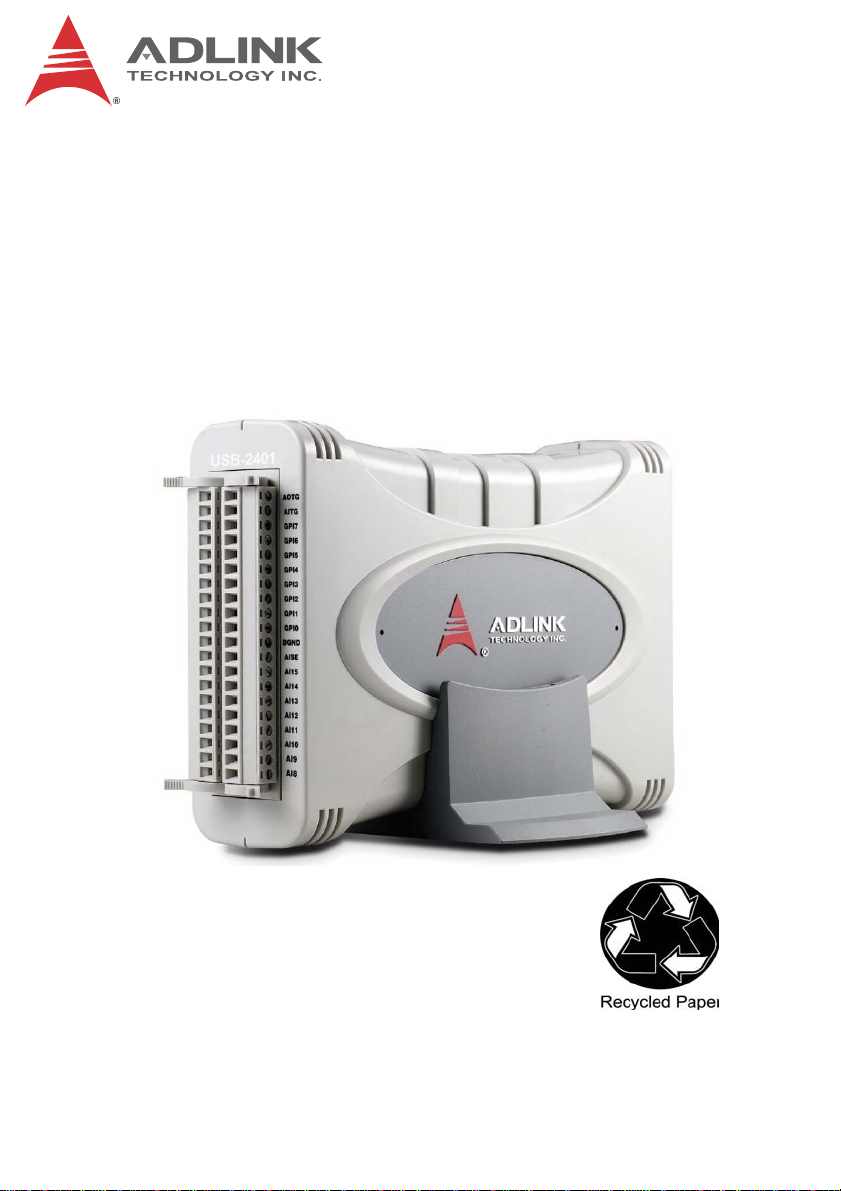
The USB-2401 is a 24-bit, 4-channel simultaneous-sampling universal input USB DAQ module featuring built-in signal conditioning
and direct measurement of commonly used sensors, including
current output transducers, thermocouple, RTD, load cell, strain
gauge, and resistance. Individual channels can be programmed to
measure different signal types.
The USB-powered USB-2401 is equipped with removable
screw-down terminals for easy device connectivity, and the
included multi-functional stand fully supports desktop, rail, or wall
mounting.
The USB-2401 is suitable for basic measurement applications
requiring high resolution and accuracy, laboratory research and
material testing environments, and industrial temperature measurement. U-Test, a free ready-to-use testing program is included
to enable operation or testing of all ADLINK USB DAQ series functions with no programming requirements.
USB-2401
1.2 Features
X High-speed USB 2.0
X USB powered
X 4-CH simultaneous-sampling analog input
X Built-in signal conditioning for high voltage/current/thermo-
couple/RTD/strain gauge/load cell/resistance measurement
X Sample rate from 20 S/s to 2 kS/s
X Functional digital I/O
X Removable screw-down terminal
X Lockable USB cable for secure connectivity
X Ready-to-use testing application (U-Test) provided
Introduction 1
Page 12
1.3 Applications
X Automotive testing
X Laboratory research
X Biotech measurement
X I/O control
1.4 Specifications
1.4.1 General Specifications
Physical, Power, and Operating Environment
Interface
Dimensions
I/O Connector Two 20-pin removable screw-down terminals
Power requirement USB power (5 V @ 400 mA)
Operating
environment
Storage environment
High speed USB 2.0 compatible, mini-USB
connector
156 (L) x 114 (W) x 41 (H) mm (6.14 X 4.49 X
1.61 in.)
Ambient temperature: 0 to 55°C
Relative humidity: 10% to 90%,
non-condensing
Ambient temperature: -20 to 70 °C
Relative humidity: 5% to 95%, non-condensing
1.4.2 General Analog Input
General
Number of channels: 4 differential input (simultaneous-sampling)
Sampling rate (sample/sec) 20, 40, 80, 160, 320, 500, 1000, 2000
Resolution 24-bit
Input coupling DC
Input mode and range
Input range or
supporting type
2Introduction
Actual input range
Page 13

USB-2401
Voltage ±25V
±12.5V
±2.5V
±312.5mV
Current ±20mA 2.5V
Thermocouple K, J, N, R, S, B, T, E 78.125mV
RTD (3-wire, 4-wire) Pt 100, Pt 1000 2.5V
Half-Bridge (120Ω, 350Ω) Max. 30mV/V 78.125mV
Full-Bridge (120Ω, 350Ω) Max. 30mV/V 78.125mV
2-Wire Resistance 30kΩ 2.5V
Excitation voltage 2.5V (for half/full-bridge mode only)
Excitation current 0.5mA for RTD mode
0.05mA for Resistance mode
Cold junction compensation
(CJC) accuracy
Operational common mode
voltage range
Overvoltage protection Power on:
FIFO buffer size 4k samples
Data transfers Programmed I/O, continuous (bulk transfer
Input impedance 1.009M for voltage input mode
± 0.5°C (after 15 minute warmup)
Voltage input mode: Vcm+Vpp/2 ≦ input
range (25V/12.5V/2.5V/ 0.3125V)
Current input mode: Vcm ≦24V
Voltage input mode: 30V
Current input mode: 60mA
Sensor input mode enable: no protection
Sensor input mode disable: 30V
Excitation voltage (EX+) and AGND: no
protection
mode)
249.5 for current input mode
±25V
±12.5V
±2.5V
±312.5mV
Introduction 3
Page 14

1.4.3 Analog Input Electrical
Temperature Draft @20SPS, in ppm/°C
Mode Gain drift Offset drift
Voltage (±25V) 1.389055871 0.043023355
Voltage (±12.5V) 1.37552178 0.075556565
Voltage (±2.5V) 1.662727273 0.030882956
Voltage (±312.5mV) 21.92878977 0.110084412
Current (±20mA) 3.270369091 0.282946284
Full-bridge 28.00370355 30.90013157
Half-bridge 33.48025514 1.750342188
Thermocouple 62.9978196 0.164409864
2-wire RTD 2.842575758 0.522492944
3-wire RTD 2.879839489 0.258840329
4-wire RTD 2.902723485 0.018656382
2-wire resistance 3.026166667 0.03246755
Temperature Draft @160SPS, in ppm/°C
Mode Gain drift Offset drift
Voltage (±25V) 1.533312973 0.084457938
Voltage (±12.5V) 1.520465436 0.134715279
Voltage (±2.5V) 1.732148674 0.054557101
Voltage (±312.5mV) 20.94809375 0.130828487
Current (±20mA) 3.488472439 0.305882921
Full-bridge 26.72626394 17.74701205
Half-bridge 35.27328612 1.748929398
4Introduction
Page 15

Mode Gain drift Offset drift
Thermocouple 105.3142618 0.193622785
2-wire RTD 2.965409564 0.512440163
3-wire RTD 2.996320076 0.240909456
4-wire RTD 2.854513258 0.086721521
2-wire resistance 3.40709375 0.06209485
Temperature Draft @2000SPS, in ppm/°C
Mode Gain drift Offset drift
Voltage (±25V) 1.620950284 0.105635778
Voltage (±12.5V) 1.584251894 0.11027477
Voltage (±2.5V) 1.701225379 0.067356314
Voltage (±312.5mV) 20.52684091 0.113061874
USB-2401
Current (±20mA) 3.771356399 0.338399386
Full-bridge 30.71138027 50.00179464
Half-bridge 35.58911174 1.862124485
Thermocouple 117.7077884 0.435895845
2-wire RTD 3.047327178 0.452466872
3-wire RTD 3.124556345 0.189605804
4-wire RTD 3.216423295 0.088365093
2-wire resistance 3.386921402 0.04574323
Introduction 5
Page 16

System Noise, in LSB (Typical, 25°C): 20 SPS to 160 SPS
Mode Sampling Rate (SPS)
20 40 80 160
Voltage (±25V) 9.443641 13.58713513 22.225423 47.06011713
Voltage (±12.5V) 10.45022375 15.55506725 23.934448 50.668689
Voltage (±2.5V) 8.941254375 12.75718938 19.522499 46.11391238
Voltage
(±312.5mV)
Current (±20mA) 29.50086975 33.76906888 39.179197 53.86180763
Full/Half-bridge 58.669068 33.97045388 41.628525 67.98029188
Thermocouple 28.24161013 41.73502813 51.59679 76.21635225
2-wire RTD 8.00126525 11.64115513 16.869046 33.30653975
3-wire RTD 8.407154625 12.01619113 16.528028 33.69525963
4-wire RTD 9.043779125 12.47814688 16.762287 45.44077163
2-wire
resistance
11.115466 15.1842875 19.108748 39.44412825
9.318955625 13.208205 18.829651 43.74764375
System Noise, in LSB (Typical, 25°C): 320 SPS to 2000 SPS
Mode Sampling Rate (SPS)
320 640 1000 2000
Voltage (±25V) 72.508028 142.60307 71.11201 119.26144
Voltage (±12.5V) 81.44560913 139.01469 77.924207 128.36732
Voltage (±2.5V) 66.64280488 136.24263 71.915341 122.92882
Voltage
(±312.5mV)
Current (±20mA) 77.58907738 131.06695 80.416917 126.239
Full/Half-bridge 92.8294875 144.14509 175.67111 202.15501
6Introduction
48.83473638 79.888989 86.157589 128.4315
Page 17

USB-2401
Mode Sampling Rate (SPS)
Thermocouple 107.9735725 143.46202 198.49927 202.17693
2-wire RTD 44.53668125 77.870435 71.369319 127.45831
3-wire RTD 42.00570563 87.738238 72.70806 123.21166
4-wire RTD 72.2785775 155.50389 72.168651 123.65813
2-wire
resistance
72.76746238 153.9091 71.566314 122.28421
1.4.4 Digital Input/Output
I/O Specifications
Number of channels 4-CH programmable function digital input (DI)
2-CH programmable function digital output
(DO)
Compatibility TTL (single-end) (supports 3.3V and 5 V DI but
3.3V DO)
Input voltage Logic low: VIL = 0.8 V max; IIL = 0.2 mA max.
Logic high: VIH = 2.0 V min.; IIH = 0.2 mA max.
Output voltage Logic low: VOL = 0.5 V max; IOL = 10 mA max.
Logic high: VOH = 2.6V min.; IIH = 10 mA max.
Supporting modes (only
one can be selected and
function at the same time,
please see Section 4.6:
Programmable Function
I/O)
X 4-CH TTL DI and 2-CH TTL
DO
X 1-CH 32-bit general-purpose
timer/counters:
Z Clock source: internal or
external
Z Max source frequency:
internal: 80 MHz; external:
10 MHz
X 1-CH PWM outputs:
Z Duty cycle:1-99% (please
see Section 4.6.3: Mode 10:
PWM Output) Modulation
frequency: 20 MHz to
0.005Hz
Introduction 7
Page 18

I/O Specifications
Data transfers Programmed I/O
1.5 Software Support
ADLINK provides comprehensive software drivers and packages
to suit various user approaches to system building. In addition to
programming libraries, such as DLLs, for most Windows-based
systems, ADLINK also provides drivers for other application environments such as LabVIEW® and MATLAB®. ADLINK also provides ActiveX component ware for measurement and
SCADA/HMI, and breakthrough proprietary software. All software
options are included in the ADLINK All-in-One CD.
Be sure to install the driver & utility before using the USB-2401
module.
1.6 Driver Support for W indows
1.6.1 UD-DASK
UD-DASK is composed of advanced 32/64-bit kernel drivers for
customized DAQ application development. USB-DASK enables
you to perform detailed operations and achieve superior performance and reliability from your data acquisition system. DASK
kernel drivers now support Windows 7/Vista® OS.
1.6.2 DAQPilot
DAQPilot is a SDK with a graphics-driven interface for various
application development environments. DAQPilot represents
ADLINK's commitment to full support of its comprehensive line of
data acquisition products and is designed for the novice to the
most experienced programmer.
As a task-oriented DAQ driver, SDK and wizard for Windows systems, DAQPilot helps you shorten development time while accelerating the learning curve for data acquisition programming.
You can download and install DAQPilot at:
http://www.adlinktech.com/TM/DAQPilot.html
8Introduction
Page 19

USB-2401
Please note that only DAQPilot versions 2.3.0.712 and later can
support the USB-2401.
Introduction 9
Page 20

1.7 Utilities for Windows
1.7.1 U-Test
U-Test is a free and ready-to-use utility which can assist instant
testing and operation of all ADLINK USB DAQ series functions
with no programming. In addition to providing data collection and
monitoring functions, U-Test also supports basic FFT analysis and
provides direct control of analog output and digital I/O with a
user-friendly interface.
A
B
C
D
Figure 1-1: U-Test Interface
A Main Menu
B Device Viewer
C AI Data View & AO, DIO Control Panel
D Analog Input Configuration
Table 1-1: U-Test Interface Legend
You can download and install U-Test at: http://www.adlinktech.com/
10 Introduction
Page 21

1.8 O verview and Dimensions
All dimensions shown are in millimeters (mm)
NOTE:
NOTE:
1.8.1 Module
USB-2401
114
41.3
Figure 1-2: USB-2401 Module Rear View
Introduction 11
Page 22

Figure 1-3: USB-2401 Module Side View
12 Introduction
Page 23

114
USB-2401
41.3
Figure 1-4: USB-2401 Module Front View
Introduction 13
Page 24

1.8.2 Module Stand
The multi-function USB-2401 stand is compatible with desk, rail, or
wall mounting. To fix the module in the stand, slide the module
body into the stand until a click is heard. To remove the module
from the stand, twist the bottom of the stand in a back-and forth
motion and separate from the module.
Figure 1-5: Module, Stand, Connector, and USB Cable
200.1
169.4
156.5
Figure 1-6: Module, Stand, & Wall Mount Kit Side View (w/ Connections)
14 Introduction
Page 25

USB-2401
Figure 1-7: Module In Stand Front View
Introduction 15
Page 26

26
B
20.4
Figure 1-8: Module Stand Top View
16 Introduction
20.4
Page 27

1.5
3.4
6
USB-2401
5.89
Figure 1-9: Module Stand Side Cutaway View
100
Figure 1-10: Module Stand Front View
Introduction 17
Page 28

1.9 Connector Information
The USB-2401 module is equipped with 40-pin removable
screw-down terminal connectors, with pin assignment and signal
description as follows.
Pin Function Pin Function
20 GPO0 40 GPO1
19 GPI1 39 GPI3
18 GPI0 38 GPI2
17 NC 37 DGND
16 GND1 36 GND3
15 SC1- 35 SC3-
14 SC1+ 34 SC3+
13 EXC1 33 EXC3
12 CI1- 32 CI3-
11 CI1+ 31 CI3+
10 AI1- 30 AI3-
9 AI1+ 29 AI3+
8 GND0 28 GND2
7 SC0- 27 SC2-
6 SC0+ 26 SC2+
5 EXC0 25 EXC2
4CI0- 24CI2-
3CI0+ 23CI2+
2 AI0- 22 AI2-
1 AI0+ 21 AI2+
Table 1-2: USB-2401 Pin Assignment
18 Introduction
Page 29

USB-2401
Signal Name Reference Direction Description
GND<0..3> -------- Ground of excitation
voltage/current, with
GND<0..3> and DGND
connected on board
DGND -------- Digital ground, DGND and
GND<0..3> are connected
on board
AI<0..4> GND I Differential analog Input
channels 0~3
CI<0..4> GND I Current input channel 0~3.
EXC<0..3> GND O Excitation output for channel
0~3; can be configured to
voltage output (2.5V) or
current output (1mA) by
software, with corresponding
ground pin GND<0..3>
SC<0..3> GND I Sensor (small signal) input
channel 0~3
GPI<0..3> DGND I Function digital input <0..3>
GPO<0..3> DGND O Function digital output <0,1>
N/C N/C N/C No connection
Table 1-3: I/O Signal Description
Introduction 19
Page 30

This page intentionally left blank.
20 Introduction
Page 31

2 Getting Started
The appropriate driver must be installed before you can connect the USB DAQ to the computer system. Refer to
WARNING:
2.1 Connecting the USB-2401 Module
Section 1.6: Driver Support for Windows for driver support
information.
1. Turn on the computer.
2. Connect the USB-2401 module to one USB 2.0 port on
the computer using the included USB cable.
3. The first time the USB-2401 module is connected, a New
Hardware message appears. It will take around 6 seconds to load the firmware. When loading is complete, the
LED indicator on the rear of the USB DAQ module
changes from amber to green and the New Hardware
message closes.
4. The USB-2401 module can now be located in the hardware Device Manager, as shown.
USB-2401
Figure 2-1: USB-2401 Module in Windows Device Manager
Getting Started 21
Page 32

If the USB-2401 module cannot be detected, the power provided
by the USB port may be insufficient. The USB-2401 module is
exclusively powered by the USB port and requires 400 mA @ 5 V.
2.2 Device ID
A rotary control on the rear of the module (as shown) controls
device ID setting and can be set from 1 to 8. The device ID allows
dedicated control of the USB-2401 module irrespective of the connected USB port. When more than one USB module of the same
type is connected, each must be set to a different ID to avoid conflicts and errors in operation.
Figure 2-2: Device ID Selection Control
22 Getting Started
Page 33

USB-2401
2.3 H ardware Configuration
All remaining hardware configurations are software
programmable, including sampling/update rate, input/output
channel, input range, and others. Please see the UD-DASK
Function Reference manual for details.
2.4 Device Mounting
2.4.1 Rail Mounting
The multi-function stand can be mounted on the DIN rail using the
rail-mount kit as shown.
Figure 2-3: Rail Mount Kit
Getting Started 23
Page 34

Figure 2-4: Module Pre-Rail Mounting
Figure 2-5: Module Rail-Mounted
24 Getting Started
Page 35

USB-2401
2.4.2 Wall Mounting
The multi-function stand can be fixed to a wall using four flush
head screws as shown. The four screw holes should be
approximately 3.4 mm in diameter.
20.4
13.0
Figure 2-6: Wall Mount Holes
Figure 2-7: Module with W al l Moun t Apparatus
Getting Started 25
Page 36

This page intentionally left blank.
26 Getting Started
Page 37

3 Operation
Operation of the USB-2401 is described here to assist in
configuration and programming of the module. Functions
described include A/D conversion, programmable function I/O,
and others
3.1 Functional Layout
The USB-2401 provides 4-channel 24-bit universal analog inputs
and supports seven input modes, including voltage input, current
input, thermocouple, RTD, full bridge, half bridge, and resistance
measurement. The four channels sample simultaneously, and
while each can be configured to a different input mode, all active
channels must be configured to the same sampling rate. In
addition, the USB-2401 also provides 6-channel programmable
digital I/O and can be configured to GPIO, GPTC, or PWM mode.
USB-2401
ADC
ADLINK
USB BUS
+5V Supply
EEPROM
Calibration
Data/
Control
3.3 2.5 1.2V
Supply
data
24MHz XTAL
Cypress
CY7C68013A
8051 Core 12/
24/48MHz
DATA
Power
DDR2 SDRAM
circuit
3.3V Supply
+5V Supply
AIn+, AIn-
CIn+, CIn-
SCn+, SCn-
INTERFACE
40P CONNECTOR
EXCn
(Cold Junction
Compensation)
CJC
4DI , 2DO
Mode
Voltage
Current
Bridge-based
RTD
Resistor
Thermocouple
Excitation Source
Current (0.5mA, 0.05mA)
±4,±2.5V
Voltage (2.5V)
AFI
ADC Front end
24 Bit
Sigma-
AFI
delta ADC
Functional I/O
GPIO
GPTC
PWM
3.3/2.5/1.2V
Control signal
n=0 ~3
AI Data and
Power
circuit
Control
I2C
Interface
Digital I/O
Controller
Calibration
Controller
FPGA Core
8051 Core
Function
Interface
Figure 3-1: USB-2401 Functional Block Diagram
3.2 S ignal Sources
3.2.1 Floating Signal Source
Not connected in any way to the existing ground system.
Devices with isolated output are floating signal sources, such as
optical isolator outputs, transformer outputs, and thermocouples.
USB 2.0
High-Speed
USB BUS
USB 2.0 INTERFACE
Operation 27
Page 38

3.2.2 Ground-Referenced Signal Source
Connected in some way to the existing ground system, to a
common ground point with respect to the USB DAQ, when the
computer is connected to the same power system. Non-isolated
output of instruments and devices connected to the existing
power systems are ground-referenced signal sources.
3.3 Signal Connection
Each analog input channel can be configured to different input
modes by the software API. Details of signal connection in
different input modes follow.
3.3.1 Voltage Input Mode
The properties of the signal to be measured must be considered.
The differential input mode provides two inputs that respond to
signal voltage difference between them. If the signal source is
ground-referenced, the differential mode can be used for the
common-mode noise rejection.
Connection of ground-referenced signal sources under differential
input mode is as shown.
USB-2401
AI+
Ground reference
signal source
AI-
Common mode noise
& ground potential
Figure 3-2: Ground-Referenced Source and Differential Input
Vcm
GND
Amplifier
Amplifier
For floating signal sources, addition of a resistor at each channel
provides a bias return path. The resistor value should be about
28 Operation
Page 39

USB-2401
100 times the equivalent source impedance, such that if the
source impedance is less than 100, the negative side of the
signal needs only be connected to GND as well as the negative
input of the Instrumentation Amplifier without any resistors.
Connection of a floating signal source to the USB-2401 in
differential input mode is as shown.
USB-2401
AI+
Floating signal source
AI-
GND
Figure 3-3: Floating Source and Differential Input
Amplifier
Amplifier
3.3.2 Current Input Mode
Current signal source can be floating or grounded reference,
converted to voltage through a precision 249.5 resistor.
Cross-voltage on the precision resistor is considered differential
signal. The differential signal pair passes through differential
amplifier buffers and is measured by the analog-to-digital
converter chip (ADC) with ±2.5 V input range.
The formula to calculate voltage-to-current conversion is:
)()(voltV
mACurrent =
6701527.18
Operation 29
Page 40

I
Figure 3-4: Current Source Connection
ƻ
3.3.3 Full Bridge and Half Bridge Input Mode
A bridge-based transducer is a passive device, requiring voltage
excitation to convert the resistive change to an electrical signal.
The USB-2401 provides a steady 2.5V excitation voltage for each
analog input channel in full bridge and half bridge modes. For
half-bridge transducer, USB-2401 has built-in precision 20k
resistors to compensate the circuit as a full-bridge transducer
measurement.
Also provided is a moving average function, a common and useful
digital filtering method of smoothing fluctuation caused by noise.
The averaging number for data can be set to 0, 2, 4, 8, or 16,
where 0 represents disabling the moving average function.
A typical four-wire connection is shown.
A dotted line represents the connection and circuit of full-bridge
mode.
NOTE:
NOTE:
30 Operation
Page 41

EXC
SC+
USB-2401
USB-2401
DC 2.5V
20kƻ
SC-
20kƻ
GND
MUX
Figure 3-5: Full Bridge and Half Bridge Connection
3.3.4 Thermocouple Input Mode
A thermocouple consists of two different conductors that produce
a voltage proportional to a temperature difference between either
end of the pair of conductors. The USB-2401 uses 78.125mV
input range to acquire the thermocouple signal, and provides a
precision built-in digital temperature sensor for cold junction compensation (CJC). CJC reading is available by software API with
data in °C. The CJC is in the USB-2401 module.
The CJC temperature sensor is housed in the USB-2401 and
requires 15 minutes’ warmup to stabilize.
NOTE:
NOTE:
Operation 31
Page 42

USB-2401
SC+
SC-
Thermocouple
Figure 3-6: Thermocouple Connection
MUX
ADC
3.3.5 RTD Input Mode
The resistance temperature detector (RTD) measures temperature by correlating the resistance of the RTD element with temperature. The USB-2401 can generate a steady 0.5 mA excitation
current source to each channel in RTD input mode to measure
cross-voltage on the RTD. The actual input range is ±2.5V with a
formula of voltage to RTD resistance conversion of:
V(volt)
)( =ΩRTD
0.0005
Since the excitation current can only drive cross-voltage up to
1.5V with good linearity, the maximum equivalent value of the RTD
resistor is limited to 3k.
The USB-2401 can support two, three, and four-wire RTD measurement. Adopting three- and four-wire connections rather than
two-wire can eliminate connection lead resistance effects from
measurement. Three-wire connection is sufficient for most purposes and most universal industrial applications. Four-wire connections are used for the most precise application requirements.
32 Operation
Page 43

USB-2401
RTD
RTD
EXC
0.5mA
SC+
MUX
SC-
GND
Figure 3-7: 4-Wire RTD Connection
0.5mA
EXC
SC+
MUX
SC-
GND
Figure 3-8: 3-Wire RTD Connection
Operation 33
Page 44

0.5mA
EXC
X
SC+
X
RTD
SC-
X
GND
X
Figure 3-9: 2-wire RTD Connection
3.3.6 Wire Resistance Mode
The USB-2401 can source precision 0.05 mA excitation current to
the resistor to be measured and use a 2.5V input range to acquire
cross-voltage on the resistor. The formula of voltage to resistance
conversion is:
MUX
USB-2401
ADC
V(volt)
)( =ΩR
0.00005
Since the excitation current can only drive the cross-voltage up to
1.5V with good linearity, the maximum equivalent value of the
resistor is limited to 30k.
34 Operation
Page 45

USB-2401
0.05mA
USB-2401
SC +
X
Resistor
MUX
SC -
ADC
X
Figure 3-10: 2-Wire Resistance Connection
3.4 A I Data Format
The acquired 24-bit A/D data is 2’s complement coded data format. Valid input ranges and optimum transfer characteristics are
as shown.
Description Bipolar Analog Input Range
Full-scale
range
Least
significant bit
FSR-1LSB 24.999997V12.4999985V2.4999997V0.3124999V 7FFFFF
±25 V ±12.5 V ±2.5 V ±0.3125V N/A
2.98uV 1.49uV 0.298uV 0.037uV N/A
Digital
Code
Midscale
+1LSB
Midscale 0 V 0 V 0 V 0 V 000000
Midscale
-1LSB
-FSR -25 V -12.5 V -2.5 V -0.3125V 800000
2.98uV 1.49uV 0.298uV 0.037 uV 000001
-2.98uV -1.49uV -0.298uV -0.3124999uV FFFFFF
Table 3-1: Analog Input Range and Output Digital Code
Operation 35
Page 46

Description
Full-scale range ±78.125 mV N/A
Least significant
bit
FSR-1LSB 78.1249907 mV 7FFFFF
Midscale
+1LSB
Midscale 0 V 000000
Midscale
-1LSB
-FSR -78.125mV 800000
Table 3-2: Analog Input Range and Output Digital Code (cont’d)
Bipolar Analog
Input Range
9.313nV N/A
9.313nV 000001
-9.313nV FFFFFF
Digital Code
3.5 ADC Sampling Rate
Sampling Rate refers to ADC internal conversion speed as set by
the user. When programming through a software API, the desired
ADC sampling rate must be set, whether for single value, using a
software polling command, or block data in continuous buffer
mode. Available sampling rates are 20SPS, 40SPS, 80SPS,
160SPS, 320SPS, 500SPS, 1000SPS, and 2000SPS.
Accuracy frequently deteriorates with increased ADC sampling
rate.
NOTE:
NOTE:
3.5.1 Software Polling Dat a Transfer (Non-Buffering Programmed I/O)
Polling mode benefits flexible timing and is suitable for retrieving
the latest data without FIFO buffering latency. The USB-2401 continuously updates the latest acquired data onto a data port for specific channels. Data not retrieved in time is overwritten with new
data without notice. As the software polling rate (here equaling
data rate) of a PC may exceed the ADC sampling rate, it is possible to receive multiple identical data before a new conversion has
36 Operation
Page 47

USB-2401
completed. Please refer to UD-DASK function reference for the
details of corresponding software API instruction.
3.5.2 Continuous Acquisition Mode
Differs from software polling mode only in the generation of block
data in continuous acquisition mode without the need to consider
data overwriting or acquiring repeat data in software polling mode.
This mode is suitable for when continuous data is to be acquired in
a fixed and precise time interval. Please note the data buffer size
must be a multiple of 128 in continuous acquisition mode. Please
refer to UD-DASK function reference for details of corresponding
software API instruction.
3.6 Programmable Function I/O
The USB-2401 supports powerful programmable I/O function provided by an FPGA chip, configurable as TTL DI/DO, 32-bit
timer/counters, and PWM output. These signals are single-ended
and 5V TTL-compliant.
3.6.1 TTL DI/DO
Programmable function I/O can be used as static TTL-compliant
4-CH digital input and 2-CH digital output. The I/O lines can be
updated by software polling, with sample and update rate fully
controlled by software timing.
Pin Function Pin Function
20 GPO0 40 GPO1
19 GPI1 39 GPI3
18 GPI0 38 GPI2
17 NC 37 DGND
Table 3-3: TTL Digital I/O Pin Definition
Operation 37
Page 48

3.6.2 General Purpose Timer/Counter
The USB-2401 is equipped with one general purpose timer/counter featuring:
X Count up/down controllable by hardware or software
X Programmable counter clock source (internal clock up to
80MHz, external clock up to 10 MHz)
X Programmable gate selection (hardware or software con-
trol)
X Programmable input and output signal polarities (high active
or low active)
X Initial Count loaded from a software API
X Current count value readable by software without affecting
circuit operation.
Pin Function Pin Function
20 GPTC_OUT0 (GPO0) 40 GPTC_OUT1 (GPO1)
19 GPTC_UD (GPI1) 39 GPTC_AUX (GPI3)
18 GPTC_CLK (GPI0) 38 GPTC_GATE (GPI2)
17 NC 37 DGND
Table 3-4: Timer/Counter Pin Definition
The timer/counter has three inputs that can be controlled via
hardware or software, clock input (GPTC_CLK), gate input
(GPTC_GATE), and up/down control input (GPTC_UD). The
GPTC_CLK input provides a clock source input to the timer/counter. Active edges on the GPTC_CLK input increment or decrement
the counter. The GPTC_UD input directs the counter to count up
or down (high: count up; low: count down), while the GPTC_GATE
input is a control signal acting as a counter enable or counter trigger signal in different applications. The GPTC_OUT then generates a pulse signal based on the timer/counter mode set.
All input/output signal polarities can be programmed by software
application. For brevity, all GPTC_CLK, GPTC_GATE, and
GPTC_OUT in the following illustrations are assumed to be active
high or rising-edge triggered.
38 Operation
Page 49

USB-2401
3.6.3 General Purpose Timer/Counter Modes
Ten programmable timer/counter modes are available. All initialize
following a software-start signal set by the software. The GPTC
software reset initializes the status of the counter and reloads
the initial value to the counter. The operation remains halted
until software start is executed again. Operations under different
modes are as follows.
Mode 1: Simple Gated-Event Counting
In this mode, the counter calculates the number of pulses on
the GPTC_CLK after a software start. Initial count can be
loaded from the software application. Current count value can
be read back by software any time with no influence on calculation. GPTC_GATE enables/disables calculation. When
GPTC_GATE is inactive, the counter halts the current count
value. Operation in which initial count = 5, countdown mode is
shown.
Software start
Gate
CLK
Count value
Figure 3-11: Mode 1-Simple Gated-Event Calculation
55 432110 ffff
Mode 2: Single Period Measurement
The counter calculates the period of the signal on
GPTC_GATE in terms of GPTC_CLK. The initial count can be
loaded from the software application. After software start, the
counter calculates the number of active edges on GPTC_CLK
between two active edges of GPTC_GATE. After the completion of the period interval on GPTC_GATE, GPTC_OUT outputs high and then current count value can be read by the
Operation 39
Page 50

software application. Operation in which initial count = 0,
count-up mode is shown.
Software start
Gate
CLK
Count value
Figure 3-12: Mode 2-Single Period Measurement
00 1234555
Mode 3: Single Pulse-Width Measurement
The counter calculates the pulse-width of the signal on
GPTC_GATE in terms of GPTC_CLK. Initial count can be
loaded from the software application. After software start, the
counter calculates the number of active edges on GPTC_CLK
when GPTC_GATE is in its active state.
After the completion of the pulse-width interval on
GPTC_GATE, GPTC_OUT outputs high and current count
value can be read by the software application. Operation in
which initial count = 0, count-up mode is shown.
Software start
Gate
CLK
Count value
Figure 3-13: Mode 3-Single Pulse-Width Measurement
40 Operation
00 1234555
Page 51

USB-2401
Mode 4: Single-Gated Pulse Generation
This mode generates a single pulse with programmable delay
and programmable pulse-width following software start. The
two programmable parameters can be specified in terms of
periods of the GPTC_CLK input by the software application.
GPTC_GATE enables/disables calculation. When
GPTC_GATE is inactive, the counter halts the current count
value. Generation of a single pulse with a pulse delay of two
and a pulse-width of four is shown.
Software start
Gate
CLK
Count value
OUT
Figure 3-14: Mode 4-Single-Gated Pulse
22 1032210
Mode 5: Single-Triggered Pulse
This mode generates a single pulse with programmable delay
and programmable pulse-width following an active
GPTC_GATE edge. These programmable parameters can be
specified in terms of periods of the GPTC_CLK input. When the
first GPTC_GATE edge triggers the single pulse, GPTC_GATE
has no effect until software start is executed again. Generation
of a single pulse with a pulse delay of two and a pulse-width of
four is shown.
Operation 41
Page 52

Gate
CLK
Software start
Count value
22103210
OUT
Figure 3-15: Mode 5-Single-Triggered Pulse
Mode 6: Re-Triggered Single Pulse Generation
This mode is similar to Mode 5 except that the counter generates a pulse following every active edge of GPTC_GATE. After
software start, every active GPTC_GATE edge triggers a single
pulse with programmable delay and pulse width. Any
GPTC_GATE triggers that occur when the prior pulse is not
completed are ignored. Generation of two pulses with a pulse
delay of two and a pulse width of four is shown.
S o f t w a r e s t a r t
G a t e
C L K
C o u n t v a l u e
O U T
22 1032102
Figure 3-16: Mode 6-Re-Triggered Single Pulse
I g n o r e d
210
32102
2
Mode 7: Single-Triggered Continuous Pulse Generation
This mode is similar to Mode 5 except that the counter generates continuous periodic pulses with programmable pulse interval and pulse-width following the first active edge of
GPTC_GATE. When the first GPTC_GATE edge triggers the
counter, GPTC_GATE has no effect until software start is executed again. Generation of two pulses with a pulse delay of
four and a pulse-width of three is shown.
42 Operation
Page 53

S o f t w a r e s t a r t
G a t e
C L K
C o u n t v a l u e
O U T
44 4321021
0321021
Figure 3-17: Mode 7-Single-Triggered Continuous Pulse
Mode 8: Continuous Gated Pulse Generation
This mode generates periodic pulses with programmable pulse
interval and pulse-width following software start. GPTC_GATE
enables/disables calculation. When GPTC_GATE is inactive,
the counter halts the current count value. Generation of two
pulses with a pulse delay of four and a pulse-width of three is
shown.
S o f t w a r e s t a r t
G a t e
C L K
C o u n t v a l u e
O U T
44 3321021
0321021
USB-2401
032
103
Figure 3-18: Mode 8-Continuous Gated Pulse
Mode 9: Edge Separation Measurement
Measures the time differentiation between two different pulse
signals. The first pulse signal is connected to GPTC_GATE
and the second signal is connected to GPTC_AUX. Clocks that
pass between the rising edge signal of two different pulses
through the 40 MHz internal clock or external clock are calculated. You can calculate the time period via the known clock
frequency. The maximum counting width is 32-bit. Decrease of
Operation 43
Page 54

the counter value in Edge Separation Measurement mode is
shown.
S o f t w a r e s t a r t
G a t e
A U X
C L K
C o u n t v a l u e
1313 12 11 9 8 7 6
10
5432111111
Figure 3-19: Mode 9-Edge Separation Measurement
Mode 10: PWM Output
The USB-1900 Series timer/counter can also simulate a PWM
(Pulse Width Modulation) output. By setting a varying amount
of Pulse_initial_cnt and Pulse_length_cnt, varying pulse frequencies (Fpwm) and duty cycles (Dutypwm) can be obtained.
PWM output is shown.
P u l s e _ I n i t i a l _ c n t = 0 x 7 P u l s e _ I e n g t h _ c n t = 0 x B
P W M O U T
T I M E B A S E
Figure 3-20: Mode 10-PWM Output
Calculation of the PWM frequency and duty cycle is as follows.
F
=
F
PWM
Duty
PWM
=
44 Operation
Timeba se
+
+
cntlengthPulsecntinitialPulse
____
cntlengthPulse
__
cntlengthPulsecntinitialPulse
____
Page 55

4 Calibration
The USB-2401 is factory-calibrated before shipment. The associated calibration constants of the TrimDACs firmware are written to
the onboard EEPROM. TrimDACs firmware is the algorithm in the
FPGA. Loading calibration constants entails loading the values of
TrimDACs firmware stored in the onboard EEPROM.
The recommended re-calibration interval is one year. Please contact your local dealer to request calibration service.
USB-2401
Calibration 45
Page 56

This page intentionally left blank.
46 Calibration
Page 57

USB-2401
Important Safety Instructions
For user safety, please read and follow all instructions,
WARNINGS, CAUTIONS, and NOTES marked in this manual
and on the associated equipment before handling/operating the
equipment.
X Read these safety instructions carefully.
X Keep this user’s manual for future reference.
X Read the specifications section of this manual for detailed
information on the operating environment of this equipment.
X When installing/mounting or uninstalling/removing
equipment:
Z Turn off power and unplug any power cords/cables.
X To avoid electrical shock and/or damage to equipment:
Z Keep equipment away from water or liquid sources;
Z Keep equipment away from high heat or high humidity;
Z Keep equipment properly ventilated (do not block or
cover ventilation openings);
Z Make sure to use recommended voltage and power
source settings;
Z Always install and operate equipment near an easily
accessible electrical socket-outlet;
Z Secure the power cord (do not place any object on/over
the power cord);
Z Only install/attach and operate equipment on stable
surfaces and/or recommended mountings; and,
Z If the equipment will not be used for long periods of time,
turn off and unplug the equipment from its power source.
Important Safety Instructions 47
Page 58

X Never attempt to fix the equipment. Equipment should only
be serviced by qualified personnel.
A Lithium-type battery may be provided for uninterrupted, backup
or emergency power.
Risk of explosion if battery is replaced with an incorrect type;
please dispose of used batteries appropriately.
WARNING:
X Equipment must be serviced by authorized technicians
when:
Z The power cord or plug is damaged;
Z Liquid has penetrated the equipment;
Z It has been exposed to high humidity/moisture;
Z It is not functioning or does not function according to the
user’s manual;
Z It has been dropped and/or damaged; and/or,
Z It has an obvious sign of breakage.
48 Important Safety Instructions
Page 59

Getting Service
Contact us should you require any service or assistance.
ADLINK Technology, Inc.
Address: 9F, No.166 Jian Yi Road, Zhonghe District
New Taipei City 235, Taiwan
ᄅקؑխࡉ৬ԫሁ 166 ᇆ 9 ᑔ
Tel: +886-2-8226-5877
Fax: +886-2-8226-5717
Email: service@adlinktech.com
Ampro ADLINK Technology, Inc.
Address: 5215 Hellyer Avenue, #110, San Jose, CA 95138, USA
Tel: +1-408-360-0200
Toll Free: +1-800-966-5200 (USA only)
Fax: +1-408-360-0222
Email: info@adlinktech.com
ADLINK Technology (China) Co., Ltd.
Address: Ϟ⍋Ꮦ⌺ϰᮄᓴ∳催⾥ᡔು㢇䏃 300 ো(201203)
300 Fang Chun Rd., Zhangjiang Hi-Tech Park,
Pudong New Area, Shanghai, 201203 China
Tel: +86-21-5132-8988
Fax: +86-21-5132-3588
Email: market@adlinktech.com
USB-2401
ADLINK Technology Beijing
Address: ࣫ҀᏖ⍋⎔Ϟഄϰ䏃 1 োⲜ߯ࡼ E ᑻ 801 ᅸ(100085)
Tel: +86-10-5885-8666
Fax: +86-10-5885-8625
Email: market@adlinktech.com
ADLINK Technology Shenzhen
Address: ⏅ഇᏖቅ⾥ᡔು催ᮄϗ䘧᭄ᄫᡔᴃು
Tel: +86-755-2643-4858
Fax: +86-755-2664-6353
Email: market@adlinktech.com
Getting Service 49
Rm. 801, Power Creative E, No. 1, B/D
Shang Di East Rd., Beijing, 100085 China
A1 2 ὐ C (518057)
2F, C Block, Bldg. A1, Cyber-Tech Zone, Gao Xin Ave. Sec. 7,
High-Tech Industrial Park S., Shenzhen, 518054 China
Page 60

ADLINK Technology, Inc. (French Liaison Office)
Address: 15 rue Emile Baudot, 91300 Massy CEDEX, France
Tel: +33 (0) 1 60 12 35 66
Fax: +33 (0) 1 60 12 35 66
Email: france@adlinktech.com
ADLINK Technology Japan Corporation
Address: ͱ101-0045 ᵅҀ䛑ҷ⬄⼲⬄䤯ފ⬎ 3-7-4
⼲⬄ 374 ɛɳ 4F
KANDA374 Bldg. 4F, 3-7-4 Kanda Kajicho,
Chiyoda-ku, Tokyo 101-0045, Japan
Tel: +81-3-4455-3722
Fax: +81-3-5209-6013
Email: japan@adlinktech.com
ADLINK Technology, Inc. (Korean Liaison Office)
Address: 昢殾柢 昢爎割 昢爎壟 1675-12 微汾瘶捒娯 8猻
8F Mointer B/D,1675-12, Seocho-Dong, Seocho-Gu,
Seoul 137-070, Korea
Tel: +82-2-2057-0565
Fax: +82-2-2057-0563
Email: korea@adlinktech.com
ADLINK Technology Singapore Pte. Ltd.
Address: 84 Genting Lane #07-02A, Cityneon Design Centre,
Singapore 349584
Tel: +65-6844-2261
Fax: +65-6844-2263
Email: singapore@adlinktech.com
ADLINK Technology Singapore Pte. Ltd. (Indian Liaison Office)
Address: 1st Floor, #50-56 (Between 16th/17th Cross) Margosa Plaza,
Margosa Main Road, Malleswaram, Bangalore-560055, India
Tel: +91-80-65605817, +91-80-42246107
Fax: +91-80-23464606
Email: india@adlinktech.com
ADLINK Technology, Inc. (Israeli Liaison Office)
Address: 6 Hasadna St., Kfar Saba 44424, Israel
Tel: +972-9-7446541
Fax: +972-9-7446542
Email: israel@adlinktech.com
50 Getting Service
 Loading...