

Page 1
USB-1900 Series
16-bit 250kS/s USB 2.0-based High-performance
DAQ Module
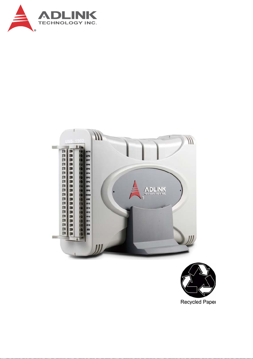
USB-1901/1902/1903
User’s Manual
Manual Rev.: 2.00
Revision Date: August 31, 2011
Part No: 50-1Z084-2000
Advance Technologies; Automate the World.
Page 2

Revision History
Revision Release Date Description of Change(s)
2.00 Aug 31, 2011 Initial release
Page 3

USB-1900 Series
Preface
Copyright 2011 ADLINK Technology Inc.
This document contains proprietary information protected by copyright. All rights are reserved. No part of this manual may be reproduced by any mechanical, electronic, or other means in any form
without prior written permission of the manufacturer.
Disclaimer
The information in this document is subject to change without prior
notice in order to improve reliability, design, and function and does
not represent a commitment on the part of the manufacturer.
In no event will the manufacturer be liable for direct, indirect, special, incidental, or consequential damages arising out of the use or
inability to use the product or documentation, even if advised of
the possibility of such damages.
Environmental Responsibility
ADLINK is committed to fulfill its social responsibility to global
environmental preservation through compliance with the European Union's Restriction of Hazardous Substances (RoHS) directive and Waste Electrical and Electronic Equipment (WEEE)
directive. Environmental protection is a top priority for ADLINK.
We have enforced measures to ensure that our products, manufacturing processes, components, and raw materials have as little
impact on the environment as possible. When products are at their
end of life, our customers are encouraged to dispose of them in
accordance with the product disposal and/or recovery programs
prescribed by their nation or company.
Trademarks
Product names mentioned herein are used for identification purposes only and may be trademarks and/or registered trademarks
of their respective companies.
iii
Page 4

Using this Manual
Audience and Scope
The USB-1900 Series User’s Manual is intended for hardware
technicians and systems operators with knowledge of installing,
configuring and operating industrial grade single board computers.
Manual Organization
This manual is organized as follows:
Preface: Presents important copyright notifications, disclaimers,
trademarks, and associated information on the proper understanding and usage of this document and its associated product(s).
Introduction: Introduces the USB-1900 Series, its features. spec-
ifications, and river information.
Hardware Information: Provides information on dimensions, con-
nection, accessories, and pin assignments for the USB-1900
Series.
Installing the USB-1900 Series Module: Describes installation
and initialization of USB-1900 Series hardware and software components.
Operation: USB-1900 Series functions described here include A/
D conversion, D/A conversion, encoder, programmable function I/
O, and others.
Calibration: This chapter introduces the calibration process to
minimize AD measurement errors and DA output errors.
Important Safety Instructions: Presents safety instructions all
users must follow for the proper setup, installation and usage of
equipment and/or software.
Getting Service: Contact information for ADLINK’s worldwide
offices.
iv
Page 5
USB-1900 Series
Conventions
Take note of the following conventions used throughout this
manual to make sure that users perform certain tasks and
instructions properly.
Additional information, aids, and tips that help users perform
tasks.
NOTE:
NOTE:
Information to prevent minor physical injury, component dam-
age, data loss, and/or program corruption when trying to com-
CAUTION:
WARNING:
plete a task.
Information to prevent serious physical injury, component
damage, data loss, and/or program corruption when trying to
complete a specific task.
v
Page 6

This page intentionally left blank.
vi
Page 7

USB-1900 Series
Table of Contents
Revision History...................................................................... ii
Preface.................................................................................... iii
List of Figures........................................................................ xi
List of Tables........................................................................ xiii
1 Introduction ........................................................................ 1
1.1 Overview.............................................................................. 1
1.2 Features............................................................................... 1
1.3 Applications ......................................................................... 2
1.4 Specifications....................................................................... 3
1.4.1 General Specifications................................................ 3
1.4.2 Analog Input ............................................................... 4
1.4.3 Analog Output............................................................. 7
1.5 Unpacking Checklist ............................................................ 8
1.6 Software Support ................................................................. 8
1.7 Driver Support for Windows................................................. 8
1.8 Utilities for Windows ............................................................ 9
2 Hardware Information...................................................... 11
2.1 Overview and Dimensions ................................................. 11
2.1.1 Module...................................................................... 11
2.1.2 Module Stand ........................................................... 14
2.1.3 Rail Mounting............................................................ 18
2.1.4 Wall Mounting........................................................... 20
2.2 Connector Pin Assignment ................................................ 21
2.2.1 Connector Signal Description ................................... 24
2.3 Analog Input Signal Connection ........................................ 24
vii
Page 8

3 Installing the USB-1900 Series Module........................... 31
3.1 Connecting the USB-1900 Series Module ......................... 31
3.2 Device ID ........................................................................... 32
3.3 Hardware Configuration ..................................................... 33
4 Operation........................................................................... 35
4.1 Signal Function .................................................................. 35
4.2 A/D Conversion.................................................................. 36
4.2.1 Analog Input Circuitry ............................................... 37
4.2.2 AI Data Format ......................................................... 37
4.2.3 Software Conversion with Polling Data Transfer
Acquisition Mode (Software Polling) ......................... 38
4.2.4 Continuous Acquisition (Scanning) Mode................. 38
4.2.5 Analog Input Triggering ............................................ 41
4.3 Trigger Sources ................................................................. 41
4.3.1 Software Triggering .................................................. 41
4.3.2 External Analog Triggering ....................................... 42
4.3.3 External Digital Triggering ........................................ 43
4.4 Trigger Modes.................................................................... 43
4.4.1 Post-Trigger Acquisition Mode (no retriggering)....... 44
4.4.2 Delayed-Trigger Acquisition Mode
(no retriggering) ........................................................ 44
4.4.4 Gated Trigger............................................................ 46
4.5 D/A Conversion.................................................................. 47
4.5.1 Bipolar Output Modes ............................................... 48
4.5.2 Software Update ....................................................... 48
4.5.3 Waveform Generation............................................... 48
4.5.4 Waveform Trigger Sources....................................... 51
4.5.5 Waveform Generation Trigger Modes ...................... 52
4.6 Programmable Function I/O............................................... 56
4.6.1 TTL DI/DO ................................................................ 56
4.6.2 General Purpose Timer/Counter............................... 57
4.7 Basic Timer/Counter Function ........................................... 57
viii
Page 9

USB-1900 Series
4.8 General Purpose Timer/Counter Modes............................ 58
4.8.1 Mode 1: Simple Gated-Event Counting .................... 58
4.8.2 Mode 2: Single Period Measurement ....................... 59
4.8.3 Mode 3: Single Pulse-Width Measurement .............. 59
4.8.4 Mode 4: Single-Gated Pulse Generation .................. 60
4.8.5 Mode 5: Single-Triggered Pulse ............................... 60
4.8.6 Mode 6: Re-Triggered Single Pulse Generation....... 61
4.8.7 Mode 7: Single-Triggered Continuous
Pulse Generation...................................................... 62
4.8.8 Mode 8: Continuous Gated Pulse Generation.......... 62
4.8.9 Mode 9: Edge Separation Measurement .................. 62
4.8.10 Mode 10: PWM Output ............................................. 63
5 Calibration......................................................................... 65
5.1 Loading Calibration Constants........................................... 65
5.2 Auto-Calibration (USB-1901/1902 only) ............................ 65
5.3 Saving Calibration Constants ............................................ 66
Important Safety Instructions.............................................. 67
Getting Service...................................................................... 69
ix
Page 10

This page intentionally left blank.
x
Page 11

USB-1900 Series
List of Figures
Figure 2-1: USB-1902 Module Rear View................................... 11
Figure 2-2: USB-1902 Module Side View ................................... 12
Figure 2-3: USB-1902 Module Front View .................................. 13
Figure 2-4: Module, Stand, Connector, and USB Cable ............. 14
Figure 2-5: Module, Stand, & Wall Mount Kit Side View
(w/ connections) ....................................................... 14
Figure 2-6: Module in Stand Front View ..................................... 15
Figure 2-7: Module Stand Top View ........................................... 16
Figure 2-8: Module Stand Side Cutaway View ........................... 17
Figure 2-9: Module Stand Front View ......................................... 17
Figure 2-10: Rail Mount Kit ........................................................... 18
Figure 2-11: Module Pre-Rail Mounting ........................................ 18
Figure 2-12: Module Rail-Mounted ............................................... 19
Figure 2-13: Wall Mount Holes ..................................................... 20
Figure 2-14: Module with Wall Mount Apparatus .......................... 20
Figure 2-15: Floating source w/ RSE input connections ............... 26
Figure 2-16: GRND-Referenced Sources w/ NRSE Inputs........... 27
Figure 2-17: GRND-Referenced Source w/ P-D Input .................. 27
Figure 2-18: Floating Source w/ P-D Input.................................... 28
Figure 2-19: Current Input............................................................. 29
Figure 3-1: USB-1900 module in Windows Device Manager...... 31
Figure 3-2: Device ID Selection Control...................................... 32
Figure 4-1: Functional Block Diagram (USB-1902)..................... 36
Figure 4-2: Analog Input ............................................................. 37
Figure 4-3: Analog Input Scan Timing ........................................ 39
Figure 4-4: Below-Low Analog Triggering................................... 42
Figure 4-5: Above-High Analog Triggering ................................. 43
Figure 4-6: Digital Triggering ...................................................... 43
Figure 4-7: Post Trigger without Retriggering ............................. 44
Figure 4-8: Delayed Trigger ........................................................ 45
Figure 4-9: Post Trigger or Delay Trigger with Retriggering ....... 46
Figure 4-10: Gated Trigger ........................................................... 47
Figure 4-11: Waveform Generation for Two Channel Update ...... 49
Figure 4-12: FIFO Data In/Out Structure ...................................... 49
Figure 4-13: Waveform Generation Hardware Timing .................. 51
Figure 4-14: Post-Trigger Waveform Generation.......................... 52
Figure 4-15: Delayed-Trigger Waveform Generation.................... 53
Figure 4-16: Post-Trigger or Delayed-Trigger with Retriggering... 54
xi
Page 12

Figure 4-17: Infinite Iteration Waveform Generation ..................... 55
Figure 4-18: Mode 1-Simple Gated-Event Calculation.................. 58
Figure 4-19: Mode 2-Single Period Measurement ........................ 59
Figure 4-20: Mode 3-Single Pulse-Width Measurement ............... 60
Figure 4-21: Mode 4-Single-Gated Pulse...................................... 60
Figure 4-22: Mode 5-Single-Triggered Pulse ................................ 61
Figure 4-23: Mode 6-Re-Triggered Single Pulse .......................... 61
Figure 4-24: Mode 7-Single-Triggered Continuous Pulse............. 62
Figure 4-25: Mode 8-Continuous Gated Pulse.............................. 62
Figure 4-26: Mode 9-Edge Separation Measurement................... 63
Figure 4-27: Mode 10-PWM Output.............................................. 63
xii
Page 13

USB-1900 Series
List of Tables
Table 2-1: USB-1901/1902 pin assignment in
single-end AI mode........................................................ 21
Table 2-2: USB-1901/1902 pin assignment in
pseudo-differential AI mode........................................... 22
Table 2-3: USB-1903 pin assignment ............................................. 23
Table 2-4: CN1/CN2 I/O Signal Description.................................... 24
Table 4-1: Bipolar Analog Input Range and Output Digital Code ... 37
Table 4-2: Bipolar Output Code ...................................................... 48
Table 4-3: Waveform Generation Timer Definition ......................... 50
Table 4-4: Pin Definition of TTL Digital I/O ..................................... 56
Table 4-5: Timer/Counter Pin Definition.......................................... 57
xiii
Page 14

xiv
This page intentionally left blank.
Page 15

USB-1900 Series
1 Introduction
1.1 Overview
The USB-1900 Series of 16-bit 250 kS/s USB 2.0-based high-performance DAQ modules includes models USB-1901/1902, featuring four different voltage input ranges, and USB-1903, with
additional built-in precision current-to-voltage resistors capable of
direct measurement of current signal from 0 to 20 mA.
The series also delivers 2-CH, 16-bit analog output capable of up
to 1 MS/s update and programmable function I/O. The software
programmable function I/O supports a variety of functions including TTL digital I/O, general-purpose timer/counter, and PWM output. The USB-1900 Series’ analog input, analog output, and
function I/O are capable of functioning simultaneously at full
speed.
The modules are USB-powered and equipped with removable
screw-down terminals for easy wiring. The attached multi-functional stand can be used for desktop, rail, or wall mounting.
Suitable for mixed-signal tests, laboratory research, and factory
automation, the USB-1900 Series provides a significant single-board solution with optimum integration of multiple tasks at an
affordable price.
1.2 Features
X High-speed USB 2.0
X USB power supply
X 16-CH voltage input and 2-CH voltage output (USB-1902)
X 16-CH voltage input (USB-1901)
X 8-CH current input and 2-CH voltage output (USB-1903)
X Up to 250 kS/s analog input
X Up to 1 MS/s analog output (USB-1902/1903)
X Programmable 8-CH digital input and 4-CH digital output
X Removable screw-down terminal module
X Lockable USB cable for secure connectivity
Introduction 1
Page 16

1.3 Applications
X Automotive testing
X Waveform generation
X Laboratory research
X Biotech measurement
X I/O control
2Introduction
Page 17

USB-1900 Series
1.4 Specifications
1.4.1 General Specifications
I/O Specifications
Number of channels 8-CH programmable function digital input (DI)
4-CH programmable function digital output
(DO)
Compatibility TTL (single-end) (supports 3.3V and 5 V DI but
3.3V DO)
Input voltage Logic low: VIL = 0.8 V max; IIL = 0.2 mA
max.Logic high: VIH = 2.0 V min.; IIH = 0.2 mA
max.
Output voltage Logic low: VOL = 0.5 V max; IOL = 10 mA max.
Logic high: VOH = 2.6V min.; IIH = 10 mA max.
Supporting modes (only one
can be selected and function
at the same time, please see
Section 4.6: Programmable
Function I/O)
Data transfers Programmed I/O
Physical, Power, and Operating Environment
Interface
Dimensions
I/O Connector Two 20-pin removable screw-down terminals
Power requirement USB power (5 V @ 400 mA)
Operating environment
Storage environment
8-CH TTL DI and 4-CH TTL DO
2-CH 32-bit general-purpose timer/counters:
Clock source: internal or external
Max source frequency: internal: 80 MHz;
external: 10 MHz
2-CH PWM outputs”:
Duty cycle:1-99% (please see
Section 4.8.10: Mode 10: PWM Output)
Modulation frequency: 20 MHz to 0.005Hz
High speed USB 2.0 compatible, mini-USB
connector
156 (L) x 114 (W) x 41 (H) mm (6.14 X 4.49 X 1.61
in.)
Ambient temperature: 0 to 55°C
Relative humidity: 10% to 90%, non-condensing
Ambient temperature: -20 to 70 °C
Relative humidity: 5% to 95%, non-condensing
Introduction 3
Page 18
1.4.2 Analog Input
Analog Input (AI)
USB-1901/1902 USB-1903
General
Number of
channels:
(programmable)
A/D converter AD7610 or equivalent
Maximum sampling rate
Resolution 16 bit
Input coupling DC
Programmable
input range
Current-to-voltage
conversion resistor
Operational common mode
voltage range
Overvoltage protection
FIFO buffer size 4k samples
Data transfers
Channel Gain Queue
configuration size
Input impedance >1 GΩ N/A
Trigger source Software, External analog or digital
Trigger mode
Time-based source Internal 80 MHz
Voltage
input
Current
Input
Volta ge
Current N/A 0~20 mA
16 single-end (SE) or 8
pseudo-differential input
N/A 8 differential
250K samples/s (single channel)
250K/N-channel samples/s (scanning)
± 10 V,± 2 V, ± 1 V,
± 200 mV
N/A 249.5 Ω
± 0.1 V
Power on: continuous ± 15 V
Power off: continuous ± 2 V
Programmed I/O, continuous
N/A
N/A
(bulk transfer
mode)
256
Post trigger, delay trigger, post trigger with
re-trigger, delay trigger with re-trigger, gated
trigger
4Introduction
Page 19

USB-1900 Series
Analog Input (AI)
USB-1901/1902 USB-1903
Electrical
Offset error (gain=1) ±0.1 mV (typical) ±0.01 mA (typical)
Gain error (gain=1) ±0.05% of FSR (typical)
–3dB small signal
bandwidth
System noise
CMRR
1
2
4
Spurious-free dynamic
range (SFDR) 2
Signal-to-noise and
distortion ratio (SINAD)
Total harmonic distortion
2
(THD)
Signal-to-noise ratio
(SNR)
Effective number of bits
(ENOB)
2
3
2
600 kHz N/A
0.3 LSB
RMS
93 dB N/A
108 dB N/A
89 dB N/A
102 dB N/A
89 dB N/A
14.5 N/A
±0.05% of FSR
(typical)
N/A
Notes:
1. Small signal bandwidth input ranges as fol-
NOTE:
NOTE:
low in Table 1
2. Input ranges for System Noise, SFDR,
SINAD, THD, and SNR as follow in Table 2
3. ENOB input ranges as follow in Table 3
4. CMRR input ranges as follow in Table 4
Introduction 5
Page 20
1. -3dB small signal bandwidth: (Typical, 25°C, single-ended)
Input Range Bandwidth (-3dB)
± 10 V 600 kHz
± 2 V 630 kHz
± 1 V 660 kHz
± 200 mV 350 kHz
2. System Noise, SFDR, SINAD, THD, SNR (Typical, 25°C, single-ended)
Input
System Noise SFDR SINAD THD SNR
Range
± 10V 0.3 LSB
± 2V 0.1 LSB
± 1V 0.4 LSB
± 200mV 0.8 LSB
RMS
RMS
RMS
RMS
108 dB 89 dB 102 dB 89 dB
98 dB 85 dB 98 dB 85 dB
94 dB 77 dB 89 dB 77 dB
79 dB 67 dB 78 dB 67 dB
3. Effective number of bits (ENOB): (Typical, 25°C,
single-ended)
Input Range ENOB
± 10V 14.5 bits
± 2V 13.9 bits
± 1V 12.5 bits
± 200mV 10.8 bits
4. CMRR (DC to 60Hz, Pseudo-differential)
Input Range CMRR
± 10V 90 dB
± 2V 110 dB
± 1V 105 dB
± 200mV 98 dB
6Introduction
Page 21

1.4.3 Analog Output
Analog Output (AO)
Number of channels 2
D/A converter DAC8871 or equivalent
Maximum update rage 1M samples
Resolution 16 bits
FIFO size 10k samples, 2-CH sharing
Data transfers
Output range ± 10V
Output coupling DC
Output impedance 0.01 (maximum)
Stability Any passive load, up to 1500pF
Power-on state Around 0V, steady-state
Electrical
Offset Error ±0.15 mV (typical)
Gain Error ±0.05% (typical)
Slew rate 20 V/µs
Rise time 0.5 µs
Fall time 0.5 µs
Settle time to 1% output error 2.5 µs
DNL < 1 LSB
INL 1 LSB or less
Output driving: ±5 mA
Power-on glitch 3.4 V for 30 ms
Programmed I/O, Continuous
USB-1900 Series
(bulk trans.)
Introduction 7
Page 22

1.5 Unpacking Checklist
Before unpacking, check the shipping carton for any damage. If
the shipping carton and/or contents are damaged, inform your
dealer immediately. Retain the shipping carton and packing
materials for inspection. Obtain authorization from your dealer
before returning any product to ADLINK. Ensure that the following items are included in the package.
X USB-1900 Series module
X Stand
X Two removable screw terminals
X USB cable (2-meter length)
X Rail mount kits
X ADLINK All-in-One CD
X User’s manual
1.6 Software Support
ADLINK provides comprehensive software drivers and packages
to suit various user approaches to system building. In addition to
programming libraries, such as DLLs, for most Windows-based
systems, ADLINK also provides drivers for other application environments such as LabVIEW® and MATLAB®. ADLINK also provides ActiveX component ware for measurement and
SCADA/HMI, and breakthrough proprietary software. All software
options are included in the ADLINK All-in-One CD.
Be sure to install the driver & utility before using the USB-1900
Series module.
1.7 Driver Support for Windows
1.7.1 UD-DASK
UD-DASK is composed of advanced 32/64-bit kernel drivers for
customized DAQ application development. USB-DASK enables
you to perform detailed operations and achieve superior performance and reliability from your data acquisition system. DASK
kernel drivers now support Windows 7/Vista® OS.
8Introduction
Page 23

USB-1900 Series
1.7.2 DAQPilot
DAQPilot is a SDK with a graphics-driven interface for various
application development environments. DAQPilot represents
ADLINK's commitment to full support of its comprehensive line of
data acquisition products and is designed for the novice to the
most experienced programmer.
As a task-oriented DAQ driver, SDK and wizard for Windows systems, DAQPilot helps you shorten development time while accelerating the learning curve for data acquisition programming.
You can download and install DAQPilot at:
http://www.adlinktech.com/TM/DAQPilot.html
Please note that only DAQPilot versions 2.3.0.712 and later can
support the USB-1900 Series.
1.8 Utilities for Windows
1.8.1 U-Test
U-Test is a free and ready-to-use utility which can assist instant
testing and operation of all ADLINK USB DAQ series functions
with no programming. In addition to providing data collection and
monitoring functions, U-Test also supports basic FFT analysis and
provides direct control of analog output and digital I/O with a
user-friendly interface.
You can download and install U-Test at: http://www.adlinktech.com/
Introduction 9
Page 24

This page intentionally left blank.
10 Introduction
Page 25
USB-1900 Series
2 Hardware Information
This chapter provides information regarding dimensions, connection, accessories, and pin assignments for the USB-1900 Series.
2.1 Overview and Dimensions
X All dimensions shown are in millimeters (mm)
X While model USB-1902 is illustrated as an
NOTE:
NOTE:
2.1.1 Module
example, all dimensions and external features
shown (excepting pin connections) are common
to all USB-1900 Series modules
Figure 2-1: USB-1902 Module Rear View
Hardware Information 11
Page 26
Figure 2-2: USB-1902 Module Side View
12 Hardware Information
Page 27

114
USB-1900 Series
41.3
Figure 2-3: USB-1902 Module Front View
Hardware Information 13
Page 28

2.1.2 Module Stand
The multi-function USB-1900 Series stand is compatible with
desk, rail, or wall mounting. To fix the module in the stand, slide
the module body into the stand until a click is heard. To remove the
module from the stand, twist the bottom of the stand in a back-and
forth motion and separate from the module.
Figure 2-4: Module, Stand, Connector, and USB Cable
200.1
169.4
156.5
Figure 2-5: Module, Stand, & Wall Mount Kit Side View (w/ connections)
14 Hardware Information
Page 29

USB-1900 Series
114.3
Figure 2-6: Module in Stand Front View
Hardware Information 15
Page 30

26
B
20.4
Figure 2-7: Module Stand Top View
16 Hardware Information
20.4
Page 31

USB-1900 Series
1.5
5.89
3.4
6
Figure 2-8: Module Stand Side Cutaway View
100
Figure 2-9: Module Stand Front View
Hardware Information 17
Page 32

2.1.3 Rail Mounting
The multi-function stand can be mounted on the DIN rail using the
rail-mount kit as shown.
Figure 2-10: Rail Mount Kit
Figure 2-11: Module Pre-Rail Mounting
18 Hardware Information
Page 33

USB-1900 Series
Figure 2-12: Module Rail-Mounted
Hardware Information 19
Page 34

2.1.4 Wall Mounting
The multi-function stand can be fixed to a wall using four flush
head screws as shown. The four screw holes should be
approximately 3.4 mm in diameter.
20.4
13.0
Figure 2-13: Wall Mount Holes
Figure 2-14: Module with Wall Mount Apparatus
20 Hardware Information
Page 35

USB-1900 Series
2.2 Connector Pin Assignment
The USB-1900 Series module is equipped with 40-pin removable
screw-down terminal connectors, with pin assignment as follows.
Pin Function Pin Function
20 ECLK 40 AOTG*
19 NC 39 AITG
18 NC 38 GPI7
17 GPO3 37 GPI6
16 GPO2 36 GPI5
15 GPO1 35 GPI4
14 GPO0 34 GPI3
13 DGND 33 GPI2
12 AGND 32 GPI1
11 *AO1 31 GPI0
10 *AO0 30 DGND
9AGND29 AISE
8 AI7 28 AI15
7 AI6 27 AI14
6 AI5 26 AI13
5 AI4 25 AI12
4AI324AI11
3 AI2 23 AI10
2AI122AI9
1AI021AI8
*NC for USB-1901
Table 2-1: USB-1901/1902 pin assignment in single-end AI mode
Hardware Information 21
Page 36

Pin Function Pin Function
20 ECLK 40 AOTG*
19 NC 39 AITG
18 NC 38 GPI7
17 GPO3 37 GPI6
16 GPO2 36 GPI5
15 GPO1 35 GPI4
14 GPO0 34 GPI3
13 DGND 33 GPI2
12 AGND 32 GPI1
11 *AO1 31 GPI0
10 *AO0 30 DGND
9 AGND 29 AISE
8 AIL3 28 AIL7
7 AIH3 27 AIH7
6 AIL2 26 AIL6
5 AIH2 25 AIH6
4 AIL1 24 AIL5
3 AIH1 23 AIH5
2 AIL0 22 AIL4
1 AIH0 21 AIH4
*NC for USB-1901
Table 2-2: USB-1901/1902 pin assignment in pseudo-differential AI mode
22 Hardware Information
Page 37

Pin Function Pin Function
40 ECLK 20 AOTG
39 NC 19 AITG
38 NC 18 GPI7
37 GPO3 17 GPI6
36 GPO2 16 GPI5
35 GPO1 15 GPI4
34 GPO0 14 GPI3
33 DGND 13 GPI2
32 AGND 12 GPI1
31 AO1 11 GPI0
30 AO0 10 DGND
29 AGND 9 AISE
28 CI3- 8 CI7-
27 CI3+ 7 CI7+
26 CI2- 6 CI6-
25 CI2+ 5 CI6+
24 CI1- 4 CI5-
23 CI1+ 3 CI5+
22 CI0- 2 CI4-
21 CI0+ 1 CI4+
Table 2-3: USB-1903 pin assignment
USB-1900 Series
Hardware Information 23
Page 38

2.2.1 Connector Signal Description
Signal Reference I/O Description
Analog input (AI) ground. All three
AIGND --------
AI<0..15> AIGND I
CI<0..7> AIGND I
AISE(AISENSE) AIGND I
AO<0, 1> AOGND O AO channel <0, 1>
GPI<0..7> DGND I
GPO<0..3> DGND O
ECLK DGND I External A/D conversion clock
AITG DGND I Digital trigger for analog input
AOTG DGND O Digital trigger for analog output
NC NC NC No connection
ground references (AIGND, AOGND,
and DGND) are connected together on
board
Analog Input Channels 0~15. Each
channel pair, AI<i, i+8> (I=0..7) can be
configured as either two single-end
inputs or one pseudo-differential input
pair (marked as AIH<0..7> and
AIL<0..7>)
CI<0..7>+ and CI<0..7>- are differential
input pairs for current Input channel
0~7.
Analog Input Sense. This pin is the
reference for any channels AI<0..63> in
NRSE input configuration
Function Input <0..7> (see Section 4.6:
Programmable Function I/O)
Function Output <0..3> (see
Section 4.6: Programmable Function I/
O)
Table 2-4: CN1/CN2 I/O Signal Description
2.3 Analog Input Signal Connection
The USB-1901 and 1902 provide up to 16 single-end or 8
pseudo-differential analog input channels. You can set the Channel to acquire the desired input signal type combination. The analog signal can be converted to a digital value by the A/D converter.
24 Hardware Information
Page 39

USB-1900 Series
To avoid ground loops and obtain more accurate measurement
from the A/D conversion, it is important to understand the type of
signal source and how to choose the analog input modes from
among Referenced single-end (RSE), Non-Referenced single-end
(NRSE), and Pseudo-Differential Input (PDIFF).
2.3.1 Signal Source Types
Floating
A floating signal source is not connected in any way to the
existing ground system. A device with an isolated output is a
floating signal source. This includes optical isolator outputs,
transformer outputs, and thermocouples.
Ground-Referenced
A ground-referenced signal is connected in some way to the
existing ground system. That is, the signal source is already
connected to a common ground point with respect to the
USB-1900 series, assuming that the computer is connected to
the same power system. Non-isolated outputs of instruments
and devices that plug into the existing power systems are
ground-referenced signal sources.
2.3.2 Input Configurations
Single-End Connections
A single-end connection is used when the analog input signal is
referenced to a ground that can be shared with other analog
input signals. There are two types of single-end connections:
RSE and NRSE configuration. In RSE configuration, the
USB-1900 Series provides the grounding point for external
analog input signals and is suitable for floating signal sources.
In NRSE configuration, the USB-1900 Series does not provide
the grounding point. The external analog input signal provides
its own reference grounding point and is suitable for
ground-referenced signals.
Referenced Single-End (RSE) Mode
In referenced single-end mode, all input signals are connected
to the ground provided by the USB-1900 Series, as shown.
Hardware Information 25
Page 40

This mode is suitable for connections with floating signal
AInA
A
sources.
When two or more floating sources are connected, these
sources will be referenced to the same common ground.
NOTE:
NOTE:
Floating
Signal
Source
V2
V1
n = 0, ...,63
Figure 2-15: Floating source w/ RSE input connections
CN1
Input Multiplexer
IGND
Instrumentation
mplifier
-
Non-Referenced Single-End (NRSE) Mode
To measure ground-referenced signal sources connected to
the same ground point, connect the signals in NRSE mode, as
shown. The signals’ local ground reference is connected to the
negative input of the instrumentation amplifier (AISENSE pin
on CN1 connector), and the common-mode ground potential
between signal ground and the ground on board is rejected by
the instrumentation amplifier.
To A / D
Converter
-
26 Hardware Information
Page 41

USB-1900 Series
A
A
x
A
A
A
A
A
Instrumentation
mplifier
+
-
Ground
Referenced
Signal
Source
Commonmode noise &
Ground
potential
V
cm
= 0, ..., 7
Input Multiplexer
IxH
IxL
IGND
Figure 2-16: GRND-Referenced Sources w/ NRSE Inputs
Pseudo-Differential Input Mode
Pseudo-differential input mode provides positive signal and
negative signal inputs that respond to signal voltage difference
between them, with the negative signal at a constant potential,
as shown. If the signal source is ground-referenced,
psuedo-differential mode can be used for noise rejection for
improvement over single-ended mode.
To A / D
Converter
-
IxH
IxL
Input Multiplexer
+
-
IGND
Instrumentation
Amplifier
To A/D
Converter
-
x = 0, ..., 7
Ground
Referenced
Signal
Source
Figure 2-17: GRND-Referenced Source w/ P-D Input
Hardware Information 27
Page 42

Connection of a floating signal source to the USB-1900 Series
A
A
A
module in pseudo-differential input mode is further shown. For
floating signal sources, the negative side of the signal should
be connected to the AIGND, with less noise coupled into the
signal connections than in single-end mode.
IxH
IxL
Input Multiplexer
+
-
IGND
Instrumentation
Amplifier
To A/D
Converter
-
x = 0, ..., 7
Floating
Signal
Source
Figure 2-18: Floating Source w/ P-D Input
Current Input Mode (for USB-1903)
The current signal source can be floating or grounded reference, and will be converted to voltage through a precision
249.5Ω resistor. Cross voltage on the precision resistor is considered differential signal. The differential signal pair passes
through differential amplifier buffers and is measured by the
analog-to-digital converter chip (ADC) with +/-10 V input range.
28 Hardware Information
Page 43

USB-1900 Series
The negative end of the differential pair is connected to the system ground after current-to-voltage conversion.
249.5
Figure 2-19: Current Input
USB-1903 includes a differential amplifier in the front-end circuit
providing support for common mode voltage of current source
NOTE:
NOTE:
up to ±24 V.
Hardware Information 29
Page 44

This page intentionally left blank.
30 Hardware Information
Page 45

USB-1900 Series
3 Installing the USB-1900 Series Module
The appropriate driver must be installed before you can connect the USB DAQ to your computer system. Refer to
WARNING:
3.1 Connecting the USB-1900 Series Module
Section 1.7: Driver Support for Windows for driver support
information.
1. Turn on your computer.
2. Connect the USB-1900 Series module to one USB 2.0
port on your computer using the included USB cable.
3. The first time the USB-1900 Series module is connected,
a New Hardware message appears. It will take around 6
seconds to load the firmware. When loading is complete,
the LED indicator on the rear of the USB DAQ module
changes from amber to green and the New Hardware
message closes.
4. The USB-1900 Series module can now be located in the
hardware Device Manager, as shown.
Figure 3-1: USB-1900 module in Windows Device Manager
Installing the USB-1900 Series Module 31
Page 46

If the USB-1900 Series module cannot be detected, the power
provided by the USB port may be insufficient. The USB-1900
Series module is exclusively powered by the USB port and
requires 400 mA @ 5 V.
3.2 Device ID
A rotary control on the rear of the module (as shown) controls
device ID setting and can be set from 1 to 8. The device ID allows
dedicated control of the USB-1900 Series module irrespective of
the connected USB port. When more than one USB module of the
same type is connected, each must be set to a different ID to avoid
conflicts and errors in operation.
Figure 3-2: Device ID Selection Control
32 Installing the USB-1900 Series Module
Page 47

USB-1900 Series
3.3 Hardware Configuration
All remaining hardware configurations are software
programmable, including sampling/update rate, input/output
channel, input range, and others. Please see the UD-DASK
Function Reference manual for details.
Installing the USB-1900 Series Module 33
Page 48

This page intentionally left blank.
34 Installing the USB-1900 Series Module
Page 49

USB-1900 Series
4 Operation
Operation of the USB-1900 Series is described here to assist in
configuration and programming of the module. Functions
described include A/D conversion, D/A conversion, programmable
function I/O, and others
4.1 Signal Function
the USB-1900 Series provides 16 single-end channels or 8
pseudo-differential channels of 16-bit A/D input, and two
single-end channels of 16-bit D/A output. Switching the multiple
front-end multiplexers allows all A/D input channels to connect to
one ADC (ADI AD7610 or equivalent). For D/A function, two
analog output channels are generated by one DAC chip (TI
DAC8871). The ADC/DAC controller and all timing control logics
are implemented by the FPGA.
The USB-1900 Series utilizes calibration circuits to provide high
performance and low-temperature drift DC signal sourcing.
Calibration data is saved in the EEPROM. Combining FIFO control
logic and simultaneous update capabilities, the USB-1902 and
USB-1903 provide 2-channel simultaneous basic waveform
generation. General purpose digital IO is controlled directly by the
FPGA, as shown.
Operation 35
Page 50

Control signal
DATA
EEPROM
EEPROM
24MHz XTAL
Cypress
CY7C68013A
8051 Core
12/24/48MHz
INTERFACE
40P CONNECTOR
16AI
2AO
8DI 4DO
General Timer/
Counter
PWM
+-13V
+5V Supply
ADC Front end
16 Bit ADC
AD7610
AFI
DAC Circuit
16 Bit DAC
DIO circuit
DI DO Circuit
General
Timer/
Counter
PWM
Power
Power
circuit
AI
Control
AI Data and
Control
Calibration
FPGA
AO
control
AO data
General Timer/Counter,
Control
Calibration
Digital I/O,
Pulse Generation
function
8051 Core
data
Calibration
Others
Figure 4-1: Functional Block Diagram (USB-1902)
4.2 A/D Conversion
When using an A/D converter, the properties of the signal to be
measured must be considered and a channel and connection of
signals to the module selected. Please see Section 2.3: Analog
Input Signal Connection. As well, A/D signal configuration,
including channel, gain, and signal type must be defined and set.
A/D acquisition is initiated by a predefined trigger source. Data
acquisition will commence once a trigger condition is matched.
After A/D conversion, A/D data is buffered in a data FIFO for
transfer into system memory for further processing.
USB INTERFACE
36 Operation
Page 51

USB-1900 Series
4.2.1 Analog Input Circuitry
AI Channel
configuration
Connection
Selection
Connect
Type
Calibration
MUX
Input Gain
Selection
PGA
REF
VOLTAGE
16Bit ADC
250ks/s
DATA
AI DATA
SPI Control
Process
Arithmetic
CGQ FIFO
AI
FIFO
4k-Sample
40-pin Screw Terminal
AI[0..15]
AISENSE
AI GND
Analog
Input
MUX
Select
FPGA
Figure 4-2: Analog Input
4.2.2 AI Data Format
The acquired 16-bit A/D data is 2’s complement coded data format. Valid input ranges and ideal transfer characteristics are
shown.
Description Bipolar Analog Input Range
Full-scale
range
±10 V ±2 V ±1 V ±0.2V
Digital
code
Least
significant
305.2uV 61.03uV 30.51uV 6.1uV
bit
FSR-1LSB 9.999695 V 1.999938 V 0.999969 V 0.199994 V 7FFF
Midscale
+1LSB
305.2 uV 61.03 uV 30.51 uV 6.1 uV 0001
Midscale 0 V 0 V 0 V 0 V 0000
Midscale
-1LSB
-305.2uV -61.03uV -30.51uV -6.1uV FFFF
-FSR -10 V -2 V -1 V -0.2V 8000
Table 4-1: Bipolar Analog Input Range and Output Digital Code
Operation 37
Page 52

For current input (USB-1903), the current signal will be converted to voltage by a precision resistor, and the input gain
WARNING:
fixed to 1(input range = ±10V), with transfer formula:
I (mA) = V (mV) / 24.89353693Ω
4.2.3 Software Conversion with Polling Data Transfer Acquisition Mode (Software Polling)
Generally the most convenient way to acquire a single A/D data
sample, the A/D converter starts a conversion when the dedicated
software command is executed. The software then polls the
conversion status and reads back the A/D data when it is
available.
This method is indicated when there is a need to process A/D data
in real time or instant closed-loop control. In this mode, the timing
of the A/D conversion is fully controlled by the software.
The A/D conversion rate is determined by the software timer
and may not be precise.
WARNING:
In Software Polling, the channel, gain, and input configuration
(RSE, NRSE, or DIFF) may be specified for each single-point
measurement. For example:
Ch2 with ± 5 V input range and single-end NRSE connection
4.2.4 Continuous Acquisition (Scanning) Mode
Continuous A/D Conversion Clock Source
When the onboard ADC receives a conversion clock signal, A/
D conversion is triggered. The USB-1900 Series conversion
clock may originate with the internal hardware timer or ECLK
(external A/D conversion clock) pin. While the conversion clock
source can be chosen by setting AI source configuration, if precision acquisition is required, use of the internal hardware timer
is recommended.
38 Operation
Page 53

USB-1900 Series
Continuous Scanning with Internal Hardware Timer
This mode is recommended if a fixed and precise A/D sampling
rate is required. You can accurately program the period
between conversions of individual channels. At least four counters must be specified, as follows.
X SI_counter (32-bit)
Specify the Scan Interval = SI_counter / timebase
X SI2_counter (32-bit)
Specify the Data Sampling Interval = SI2_counter/timebase
X PSC_counter (32-bit)
Specify the Post Scan Calculates after a trigger event
X NumChan_counter (32-bit)
Specify the number of samples per scan
Acquisition timing and meaning of the four counters are as follows.
Figure 4-3: Analog Input Scan Timing
Operation 39
Page 54

Timebase Clock Source
In scan acquisition mode, all A/D conversions start with the output of counters using the timebase as the clock source.
Through the software, you can specify the timebase as the
internal clock source (onboard 80 MHz).
Three trigger sources are available to start the scan acquisition. Refer to Section 4.3: Trigger Sources for details. For data
transfer mode, please see Section 4.2.4: Continuous Acquisition (Scanning) Mode.
X The maximum A/D sampling rate is 250 kHz. The minimum
setting for the SI2_counter when using the internal timebase is 320.
X Both the SI_counter and SI2_counter are 32-bit. The maxi-
mum sampling interval between two channels using the
32
internal timebase = 2
/80 Ms =53.687s for single channel
data acquisition.
X The scan interval must not be less than the product of the
data sampling interval and the NumChan_counter value.
The relationship can be represented as:
SI_counter>=SI2_counter *NumChan_counter.
Specifying Channels, Gains, and Input Configurations in the
Channel Gain Queue
The channel, gain, and input configurations can be specified in
the channel gain queue under Scan Acquisition mode.
In scan acquisition mode the number of entries in the Channel
Gain Queue is normally equivalent to the value of
NumChan_counter (the number of samples per scan).
40 Operation
Page 55

USB-1900 Series
Example:
1. Set:
X SI2_counter = 320
X SI_counter = 1280
X PSC_counter = 3
X NumChan_counter = 4
X timebase = Internal clock source
X Channel entries in the Channel Gain Queue: ch1, ch2, ch0,
ch2
2. Then:
X Acquisition sequence of channels: 1, 2, 0, 2, 1, 2, 0, 2, 1,
2,0, 2
X Sampling Interval = 320/80M s = four us
X Scan Interval = 1280/80M s = 16 us
X Equivalent sampling rate of ch0, ch1: 62.5 kHz
X Equivalent sampling rate of ch2: 125 kHz
4.2.5 Analog Input Triggering
The USB-1900 Series supports flexible trigger sources for analog input functionality. The trigger source can originate with
software command, external analog, or external digital signal in
continuous analog input mode. Users can configure the trigger
source and trigger mode by software.
4.3 Trigger Sources
4.3.1 Software Triggering
This trigger mode requires no external trigger source. The trigger
asserts immediately following execution of the specified function
calls to begin the operation.
Operation 41
Page 56

4.3.2 External Analog Triggering
The analog multiplexer can select one input channel as the analog
trigger source. That is, one of 16 input channels in single-end
mode (or 8 input channels in pseudo-differential mode) can be
selected as the analog trigger source. An external analog trigger
occurs when the analog trigger signal crosses above (above high)
or below (below low) the pre-defined voltage level. The range of
trigger level is the full-scale range of the selected input channel
and the resolution is 16-bit. In external analog trigger mode, the
first acquired data starts with a delay of 4 microseconds.
Below-Low Analog Triggering
In below-low analog triggering, as shown, the trigger signal is
generated when the input analog signal is less than the
Low_Threshold voltage. High_Threshold setting is not used in
this triggering situation.
Figure 4-4: Below-Low Analog Triggering
Above-High Analog Triggering
In above-high analog triggering, as shown, the trigger signal is
generated when the input analog signal exceeds the
High_Threshold voltage. Low_Threshold setting is not used in
this triggering situation
42 Operation
Page 57

USB-1900 Series
Figure 4-5: Above-High Analog Triggering
4.3.3 External Digital Triggering
An external digital trigger occurs when a rising or falling edge is
detected on the digital signal connected to the AITG (analog input
trigger) pin. Trigger polarity can be programmed using ADLINK
software drivers.
Signal level of the external digital trigger signals should be
TTL-compatible, with a minimum pulse of 20ns.
WARNING:
Positi ve-edge (rising)
t r i gger event occu r s
Negati ve-edge (f all ing)
t r i gger event occ ur s
Figure 4-6: Digital Triggering
4.4 Trigger Modes
Analog input supports post, delay, gate, post trigger with retrigger,
and delay trigger with retrigger modes.
Operation 43
Page 58

4.4.1 Post-Trigger Acquisition Mode (no retriggering)
Post-trigger acquisition is indicated in applications where data is to
be collected after a trigger event. The number of scans for each
channel after triggering is specified in the PSC_counter as shown.
The total acquired data length = NumChan_counter *
PSC_counter.
Figure 4-7: Post Trigger without Retriggering
4.4.2 Delayed-Trigger Acquisition Mode (no retriggering)
Delayed-trigger acquisition is indicated to delay data collection
after the occurrence of a specified trigger event. The delay time is
controlled by the value, pre-loaded in the Delay_counter (16nn).
The counter calculates down on the rising edge of the
Delay_counter clock source after the trigger condition is met. The
clock source can be software programmed by the timebase clock
(80 MHz). When the count reaches 0, the counter stops and the
44 Operation
Page 59

USB-1900 Series
USB-1900 Series starts to acquire data. The total acquired data
length = NumChan_counter * PSC_counter.
When the Delay_counter clock source is set to timebase, the
maximum delay time = 2
WARNING:
Trigger
Scan_ start
AD_conversion
Acquisition_in_progress
Operation start
32
/80M s = 18.626ms
(NumChan _Counter=4, PSC_Counter=3)
Delay until
Delay_Counter
reaches 0
Acquired & Stored Data
(3 scans)
Figure 4-8: Delayed Trigger
4.4.3 Post-Trigger or Delayed-Trigger Acquisition with Retriggering
Post-trigger or Delayed-Trigger acquisition with re-trigger function
is indicated where you want to collect data after several trigger
events. The number of scans after each trigger is specified in
PSC_counter, and Retrig_no can be programmed to specify the
re-trigger numbers. An example is shown, in which two scans of
data are acquired after the first trigger signal, after which the
USB-1900 Series waits for the next re-trigger signal (re-trigger sig-
Operation 45
Page 60

nals occurring before the first two scans are completed will be
ignored). When the re-trigger signal occurs, two more scans are
performed. The process repeats until the specified number of
re-trigger signals are detected. The total acquired data length =
NumChan_counter * PSC_counter * Retrig_no.
UC_count = 3, IC_count = 2, Trig_count = 3, DLY1_count disabled, DLY2_count
Trigger
DAWR
WF_in_Prog
Wave
Single waveform
3 update counts and 2 iterations
disabled
UC_Counter = 3
Ignored
Figure 4-9: Post Trigger or Delay Trigger with Retriggering
4.4.4 Gated Trigger
Gated-trigger acquisition is indicated in applications where you
want to collect data when trigger events are set to level high/low,
and hold acquisition when trigger events are set to the opposite
level.
The total number of scans for each channel is specified in the
PSC_counter. As shown, after the operation starts, the first scan of
data is immediately acquired when the trigger signal is deasserted
and paused at the second scan when the trigger signal is
asserted.
The four remaining scans are not performed until the trigger signal
is deasserted again. The process repeats until the specified
amount of retrigger signals is detected.
46 Operation
Page 61

USB-1900 Series
Total acquired data length = NumChan_counter * PSC_counter.
(NumChain_Counter=4, PSC_Counter=2)
ACQ_EN
Trigger
Scan_start
AD_conversion
Acquisition_in_progress
Acquisition Paused
Operation Start
Acquired & Stored Data
(6 scans)
Figure 4-10: Gated Trigger
4.5 D/A Conversion
For complex applications, the USB-1900 Series offers software
polling to update the output, and continuous mode to generate
waveforms. This means that the D/A update rate is controlled not
only by software timing, but can also be set by a specified
precision hardware timer. The following sections discuss the
USB-1900 Series D/A architecture and control methods.
Operation 47
Page 62

4.5.1 Bipolar Output Modes
The USB-1900 Series supports a maximum ±10 V voltage output.
The relationship of straight binary coding between the digital
codes and output voltages is as shown.
Digital Code Analog Output
0x7FFF +9.999695 V (+10 V - 1 LSB)
0x0001 +0.000305 V (1 LSB)
0x0000 0 V
0xFFFF -0.000305 V (0 V – 1 LSB)
0x8000 -10 V
Table 4-2: Bipolar Output Code
4.5.2 Software Update
This method is indicated when there is a need to generate D/A
output controlled by user programs. In this mode, the D/A converter generates one output once the software command is
issued.
Difficulty in determining the software update rate may occur
within a multitasking environment such as Windows.
WARNING:
4.5.3 Waveform Generation
Waveform Generation Data Structure
FIFO is a hardware first-in first-out data queue that holds temporary digital codes for D/A conversion. When the USB-1900
Series operates in waveform generation mode, the waveform
patterns are stored in FIFO with 10k samples. Continuous
mode transfers data according to channel order. DA channel 0
to channel 1 data is shown.
48 Operation
Page 63

USB-1900 Series
512 Samples Data FIFO
0002
……
CH1
……
Data Out
Destination
Channel
16 Bit Hex Data Format
FFFF 0000 FFFE 0001 FFFD FF 00 00FF
CH0 CH1 CH0 CH1 CH0 CH0 CH1
Figure 4-11: Waveform Generation for Two Channel Update
Data format in FIFO is shown.
DA Channel 0
DA Channel 1
WARNING:
FFFF
FFFE
0000
0001
FFFD
0002
…………
…………
Figure 4-12: FIFO Data In/Out Structure
While waveform patterns exceeding the 10k samples are also
supported in continuous mode, the output data may not be
updated in the fixed time interval if the USB bus is busy.
With hardware-based waveform generation, D/A conversions
are updated automatically by the FPGA rather than by the
application software. Compared with conventional software-based waveform generation, the precise hardware timing
control guarantees non-distorted waveform generation based
on a given and fixed time interval.
Data In
FF00
00FF
In waveform generation mode, both DACs must be configured
in the same mode. However, individual DACs can be disabled.
WARNING:
Waveform Generation Clock Source
When the onboard DAC receives a conversion clock signal, a
D/A update is triggered. The USB-1902/1903 update clock
originates with the 80 MHz internal hardware timer.
Operation 49
Page 64

Waveform Generation with Internal Hardware Timer
Six counters interact with the waveform, generating different
DAWR timings to produce various waveforms, as shown.
Counter Wid th Description Note
Update interval,
UI_counter 32-bit
UC_counter 32-bit
IC_counter 32-bit
DLY1_counter 32-bit
DLY2_counter 32-bit
Trig_counter 32-bit
defining the update
interval between each
data output.
Update count, defining
the amount of data in a
waveform.
Iteration calculation,
defining how many
times the waveform is
generated.
Defines the delay time
for waveform
generation after the
trigger signal.
Defines the delay time
to separate consecutive
waveform generation.
Effective only in
Iterative Waveform
Generation mode.
Defines the acceptable
start trigger count when
re-trigger function is
enabled
Update interval =
UI_counter / timebase*
When value in
UC_counter is less
than the size of
waveform patterns, the
waveform is generated
incrementally.
Delay Time =
(DLY1_counter / Clock
timebase)
Delay Time =
(DLY2_counter / Clock
timebase)
*timebase= 80 MHz
Table 4-3: Waveform Generation Timer Definition
50 Operation
Page 65

WARNING:
Trigger
DAWR
WF_in_Prog
USB-1900 Series
The maximum D/A update rate is 1 MHz, and the minimum
UI_counter setting is 80.
4 Update Count and 3 iteration count
UC_Counter = 4
Delay until DLY1_Counter
Reaches 0
Wave
DA_Update_Interval T =
UI_Counter / Timebase
Delay until DLY2_Counter
Reaches 0
Delay until DLY2_Counter
Reaches 0
Figure 4-13: Waveform Generation Hardware Timing
Waveform Generation Triggering
The USB-1902/1903 supports flexible trigger sources for analog output functionality. The trigger source can originate with
software or external digital signal in continuous waveform generation mode. Users can configure the trigger source and trigger mode by software.
4.5.4 Waveform Trigger Sources
Software Triggering
This trigger mode requires no external trigger source. The trigger asserts immediately following execution of the specified
function calls to begin the operation.
Operation 51
Page 66

External Digital Triggering
An external digital trigger occurs when a rising edge or falling
edge is detected on the digital signal connected to the AOTG
(Analog output trigger) pin, as shown. Users can program the
trigger polarity through ADLINK software. The signal level of
the external digital trigger signals should be TTL-compatible,
and the minimum pulse 20 ns.
4.5.5 Waveform Generation Trigger Modes
The analog output supports post, delay, post trigger with retrigger,
and delay trigger with retrigger modes.
Post-Trigger Waveform Generation
Post-trigger generation is indicated to generate a waveform
immediately following a trigger signal. The number of patterns
to be updated after the trigger signal is specified by
UC_counter * IC_counter, as shown.
8 update counts, 1 iteration
(UC _Counter=8, IC_Counter=1)
Trigger
DAWR
WFG_in_progress
Output Waveform
Operation start
6
4
2
0
3
-4
4
-2
Figure 4-14: Post-Trigger Waveform Generation
52 Operation
Page 67

USB-1900 Series
Delayed-Trigge r Waveform Generation
Delayed-Triggering is indicated when waveform generation is
to be delayed after the trigger signal. The delay time is determined by DLY1_counter, as shown. The counter calculates
down on the rising edges of DLY1_counter clock source after
the start trigger signal. When the count reaches zero, the
waveform is generated. The DLY1_counter clock source can
be selected via software application using the internal 80 MHz
timebase.
6 update count and 1 iteration count
Trigger
DAWR
WF_in_Prog
Wave
Delay until DLY1_Counter
reaches 0
UC_Counter = 6
Figure 4-15: Delayed-Trigger Waveform Generation
Post-Trigger or Delayed-Trigger with Retriggering
Post-trigger or delayed-trigger with retrigger modes are indicated when multiple waveforms are to be generated with
respect to multiple incoming trigger signals. You can set
Trig_counter to specify the number of acceptable trigger signals, as shown.
In this example, two waveforms are generated after the first
trigger signal. The USB-1902/1903 then waits for another trigger signal. When the next trigger signal is asserted, the
USB-1902/1903 generates two more waveforms.
Operation 53
Page 68

After two trigger signals, as specified in Trig_Counter, no more
trigger signals will be accepted unless a trigger reset command
is executed. For more information on the Iterative Waveform
Generation in this example, please see the next section.
UC_count = 3, IC_count = 2, Trig_count = 3, DLY1_count disabled, DLY2_count
Trigger
DAWR
WF_in_Prog
Wave
Single waveform
3 update counts and 2 iterations
disabled
UC_Counter = 3
Ignored
Figure 4-16: Post-Trigger or Delayed-Trigger with Retriggering
Start trigger signals asserted during waveform generation will
be ignored.
WARNING:
Iterative Waveform Generation
You can set the IC_counter to generate iterative waveforms
regardless of the trigger mode used. The IC_counter stores the
iteration number, as shown in the following two examples.
When the IC_counter is disabled, waveform generation will
continue until the counter is reset.
WARNING:
54 Operation
Page 69

USB-1900 Series
An onboard data FIFO buffers the waveform patterns for waveform generation. If the size of a single waveform is less than
that of the FIFO, after initially loading the data from the host
computer’s memory, the data in FIFO can be reused when a
single waveform generation is completed and will not subsequently occupy USB bandwidth.
However, if the size of a single waveform exceeds that of the
FIFO, it must be intermittently loaded from the host computer’s
memory via USB peripheral controller, and will occupy USB bandwidth.
If the value specified in the UC_counter is less than the sample
size of the waveform patterns, the waveform is generated incrementally. For example, if a 16-sample sine wave is defined and the
UC_counter set to 2, the generated waveform will be a 1/8-cycle
sine wave for every waveform period, and a complete sine wave
generated for every 8-iterations. If a UC_counter value is specified
that exceeds the sample size of the waveform LUT (for example,
32), the generated waveform will be a 2-cycle sine wave for every
waveform period.
(UC_counter = 4, IC_counter = infinite, DLY2_counter = 0)
Trigger
DAWR
WF_in_Prog
Wave
4 update count, iterate infinite
UC_Counter = 4
Single waveform
Figure 4-17: Infinite Iteration Waveform Generation
Operation 55
Page 70

In conjunction with different trigger modes and counter setups, you
can manipulate a single waveform to generate different and more
complex waveforms.
DLY2_Counter in Iterative Waveform Generation
To expand the flexibility of iterative waveform generation, the
DLY2_counter separates consecutive waveform generations.
The DLY2_counter starts counting down immediately following
a single waveform generation. When it reaches zero, the next
iteration of waveform generation will start, as shown. If the
waveform is generated incrementally, the next waveform will be
generated. The DLY2_counter clock source originates with the
internal 80 MHz timebase.
4.6 Programmable Function I/O
The USB-1900 Series supports powerful programmable I/O function provided by an FPGA chip, configurable as TTL DI/DO, 32-bit
timer/counters, and PWM output. These signals are single-ended
and 5 V TTL-compliant.
4.6.1 TTL DI/DO
Programmable function I/O can be used as static TTL-compliant
8-CH digital input and 4-CH digital output. You can read/write
these I/O lines by software polling, with sample and update rate
fully controlled by software timing.
Pin Function Pin Function
38 GPI7
17 GPO3 37 GPI6
16 GPO2 36 GPI5
15 GPO1 35 GPI4
14 GPO0 34 GPI3
13 DGND 33 GPI2
32 GPI1
31 GPI0
30 DGND
Table 4-4: Pin Definition of TTL Digital I/O
56 Operation
Page 71

USB-1900 Series
4.6.2 General Purpose Timer/Counter
The USB-1900 Series is equipped with two general purpose timer/
counter sets featuring:
X Count up/down controllable by hardware or software
X Programmable counter clock source (internal clock up to 80
MHz, external clock up to 10 MHz)
X Programmable gate selection (hardware or software con-
trol)
X Programmable input and output signal polarities (high active
or low active)
X Initial Count loaded from a software application
X Current count value readable by software without affecting
circuit operation.
Pin Function Pin Function
38 GPTC_AUX2
17 GPTC_OUT3 37 GPTC_GATE2
16 GPTC_OUT2 36 GPTC_UD2
15 GPTC_OUT1 35 GPTC_CLK2
14 GPTC_OUT0 34 GPTC_AUX0
13 DGND 33 GPTC_GATE0
32 GPTC_UD0
31 GPTC_CLK
30 DGND
Table 4-5: Timer/Counter Pin Definition
4.7 Basic Timer/Counter Function
Each timer/counter has three inputs that can be controlled via
hardware or software. They are clock input (GPTC_CLK), gate
input (GPTC_GATE), and up/down control input (GPTC_UD). The
GPTC_CLK input provides a clock source input to the timer/counter. Active edges on the GPTC_CLK input increment or decrement
the counter. The GPTC_UD input directs the counter to count up
Operation 57
Page 72

or down (high: count up; low: count down), while the GPTC_GATE
input is a control signal acting as a counter enable or counter trigger signal in different applications. The GPTC_OUT then generates a pulse signal based on the timer/counter mode set.
All input/output signal polarities can be programmed by software
application. For brevity, all GPTC_CLK, GPTC_GATE, and
GPTC_OUT in the following illustrations are assumed to be active
high or rising-edge triggered.
4.8 General Purpose Timer/Counter Modes
Ten programmable timer/counter modes are available. All modes
initialize following a software-start signal set by the software. The
GPTC software reset initializes the status of the counter and
reloads the initial value to the counter. The operation remains
halted until software start is executed again. Operations under different modes are described as follows.
4.8.1 Mode 1: Simple Gated-Event Counting
In this mode, the counter calculates the number of pulses on the
GPTC_CLK after a software start. Initial count can be loaded from
the software application. Current count value can be read back by
software any time with no influence on calculation. GPTC_GATE
enables/disables calculation. When GPTC_GATE is inactive, the
counter halts the current count value. Operation in which initial
count = 5, countdown mode is shown.
Software start
Gate
CLK
Count value
Figure 4-18: Mode 1-Simple Gated-Event Calculation
58 Operation
55 432110 ffff
Page 73

USB-1900 Series
4.8.2 Mode 2: Single Period Measurement
The counter calculates the period of the signal on GPTC_GATE in
terms of GPTC_CLK. The initial count can be loaded from the software application. After software start, the counter calculates the
number of active edges on GPTC_CLK between two active edges
of GPTC_GATE. After the completion of the period interval on
GPTC_GATE, GPTC_OUT outputs high and then current count
value can be read by the software application. Operation in which
initial count = 0, count-up mode is shown.
Software start
Gate
CLK
Count value
Figure 4-19: Mode 2-Single Period Measurement
00 1234555
4.8.3 Mode 3: Single Pulse-Width Measurement
The counter calculates the pulse-width of the signal on
GPTC_GATE in terms of GPTC_CLK. Initial count can be loaded
from the software application. After software start, the counter calculates the number of active edges on GPTC_CLK when
GPTC_GATE is in its active state.
After the completion of the pulse-width interval on GPTC_GATE,
GPTC_OUT outputs high and current count value can be read by
the software application. Operation in which initial count = 0,
count-up mode is shown.
Operation 59
Page 74

Software start
Gate
CLK
Count value
Figure 4-20: Mode 3-Single Pulse-Width Measurement
00 1234555
4.8.4 Mode 4: Single-Gated Pulse Generation
This mode generates a single pulse with programmable delay and
programmable pulse-width following software start. The two programmable parameters can be specified in terms of periods of the
GPTC_CLK input by the software application. GPTC_GATE
enables/disables calculation. When GPTC_GATE is inactive, the
counter halts the current count value. Generation of a single pulse
with a pulse delay of two and a pulse-width of four is shown.
Software start
Gate
CLK
Count value
OUT
22 1032210
Figure 4-21: Mode 4-Single-Gated Puls e
4.8.5 Mode 5: Single-Triggered Pulse
This mode generates a single pulse with programmable delay and
programmable pulse-width following an active GPTC_GATE edge.
These programmable parameters can be specified in terms of
60 Operation
Page 75

USB-1900 Series
periods of the GPTC_CLK input. When the first GPTC_GATE
edge triggers the single pulse, GPTC_GATE has no effect until
software start is executed again. Generation of a single pulse with
a pulse delay of two and a pulse-width of four is shown.
Software start
Gate
CLK
Count value
22 103210
OUT
Figure 4-22: Mode 5-Single-Triggered Pulse
4.8.6 Mode 6: Re-Triggered Single Pulse Generation
This mode is similar to Mode 5 except that the counter generates
a pulse following every active edge of GPTC_GATE. After software start, every active GPTC_GATE edge triggers a single pulse
with programmable delay and pulse width. Any GPTC_GATE triggers that occur when the prior pulse is not completed are ignored.
Generation of two pulses with a pulse delay of two and a pulse
width of four is shown.
S o f t w a r e s t a r t
G a t e
C L K
C o u n t v a l u e
O U T
22 1032102
Figure 4-23: Mode 6-Re-Triggered Single Pulse
I g n o r e d
210
32102
2
Operation 61
Page 76

4.8.7 Mode 7: Single-Triggered Continuous Pulse Generation
This mode is similar to Mode 5 except that the counter generates continuous periodic pulses with programmable pulse interval and pulse-width
following the first active edge of GPTC_GATE. When the first
GPTC_GATE edge triggers the counter, GPTC_GATE has no effect until
software start is executed again. Generation of two pulses with a pulse
delay of four and a pulse-width of three is shown.
S o f t w a r e s t a r t
G a t e
C L K
C o u n t v a l u e
O U T
44 4321021
Figure 4-24: Mode 7-Single-Triggered Continuous Pulse
0321021
032
4.8.8 Mode 8: Continuous Gated Pulse Generation
This mode generates periodic pulses with programmable pulse interval
and pulse-width following software start. GPTC_GATE enables/disables
calculation. When GPTC_GATE is inactive, the counter halts the current
count value. Generation of two pulses with a pulse delay of four and a
pulse-width of three is shown.
S o f t w a r e s t a r t
G a t e
C L K
C o u n t v a l u e
O U T
44 3321021
0321021
103
Figure 4-25: Mode 8-Continuous Gated Pulse
4.8.9 Mode 9: Edge Separation Measurement
Measures the time differentiation between two different pulse signals.
The first pulse signal is connected to GPTC_GATE and the second signal
is connected to GPTC_AUX. Clocks that pass between the rising edge
signal of two different pulses through the 40 MHz internal clock or external clock are calculated. You can calculate the time period via the known
62 Operation
Page 77

USB-1900 Series
clock frequency. The maximum counting width is 32-bit. Decrease
of the counter value in Edge Separation Measurement mode is
shown.
S o f t w a r e s t a r t
G a t e
A U X
C L K
C o u n t v a l u e
1313 12 11 9 8 7 6
10
5432111111
Figure 4-26: Mode 9-Edge Separation Measurement
4.8.10 Mode 10: PWM Output
The USB-1900 Series timer/counter can also simulate a PWM
(Pulse Width Modulation) output. By setting a varying amount of
Pulse_initial_cnt and Pulse_length_cnt, varying pulse frequencies
(Fpwm) and duty cycles (Dutypwm) can be obtained. PWM output
is shown.
P u l s e _ I n i t i a l _ c n t = 0 x 7 P u l s e _ I e n g t h _ c n t = 0 x B
P W M O U T
T I M E B A S E
Figure 4-27: Mode 10-PWM Output
Calculation of the PWM frequency and duty cycle is as follows.
F
=
F
PWM
Duty
Operation 63
PWM
=
Time base
+
cntlengthPulsecntinitialPulse
____
cntlengthPulse
__
cntlengthPulsecntinitialPulse
+
____
Page 78

This page intentionally left blank.
64 Operation
Page 79

USB-1900 Series
5 Calibration
This chapter introduces the calibration process to optimize AD
conversion and avoid DA output errors.
5.1 Loading Calibration Constants
The USB-1900 Series is factory-calibrated before shipment. The
associated calibration constants of the TrimDACs firmware are
written to the onboard EEPROM. TrimDACs firmware is the algorithm in the FPGA. Loading calibration constants entails loading
the values of TrimDACs firmware stored in the onboard EEPROM.
ADKLINK provides a software utility that automatically reads the
calibration constants, if necessary.
Dedicated space for storing calibration constants is provided in the
EEPROM. In addition to the default bank of factory calibration constants, there is one user-utilization bank, allowing loading of the
TrimDACs firmware values either from the original factory calibration or a subsequently-performed calibration.
Since measurement and output errors may vary depending on
time and temperature, it is recommended that you calibrate the
USB-1900 Series module in your existing testing environment, as
follows.
5.2 Auto-Calibration (USB-1901/1902 only)
USB-1902 auto-calibration utility measures and corrects almost all
calibration errors with no external signal connections, reference
voltage, or measurement devices. The USB-1900 Series provides
onboard calibration reference to ensure the accuracy of auto-calibration. The reference voltage is measured in the production line
by a digital potentiometer and compensated in the software. The
calibration constant is stored after this measurement.
Calibration 65
Page 80

The USB-1903, requiring an external precision current source
to calibrate the current-to-voltage conversion resistor and the
NOTE:
NOTE:
differential buffer in its front-end circuit, does not support autocalibration. Please return the module for calibration service if
necessary.
5.3 Saving Calibration Constants
Factory-calibrated constants are permanently stored in a bank of
the onboard EEPROM and cannot be modified. When the device
is recalibrated, the software stores the new constants in a userconfigurable section of the EEPROM. To restore original factory
calibration settings, the software can copy the factory-calibrated
constants to the user-configurable section of the EEPROM. When
auto-calibration is complete, the new calibration constants can be
saved to the user-configurable banks in the EEPROM.
X The USB-1900 Series should be warmed up for
at least 15 minutes before initiating auto-calibra-
NOTE:
NOTE:
tion
X Remove the cable before auto-calibrating the
card since the DA outputs are changed during
the process
66 Calibration
Page 81

USB-1900 Series
Important Safety Instructions
For user safety, please read and follow all instructions,
WARNINGS, CAUTIONS, and NOTES marked in this manual
and on the associated equipment before handling/operating the
equipment.
X Read these safety instructions carefully.
X Keep this user’s manual for future reference.
X Read the specifications section of this manual for detailed
information on the operating environment of this equipment.
X When installing/mounting or uninstalling/removing
equipment:
Z Turn off power and unplug any power cords/cables.
X To avoid electrical shock and/or damage to equipment:
Z Keep equipment away from water or liquid sources;
Z Keep equipment away from high heat or high humidity;
Z Keep equipment properly ventilated (do not block or
cover ventilation openings);
Z Make sure to use recommended voltage and power
source settings;
Z Always install and operate equipment near an easily
accessible electrical socket-outlet;
Z Secure the power cord (do not place any object on/over
the power cord);
Z Only install/attach and operate equipment on stable
surfaces and/or recommended mountings; and,
Z If the equipment will not be used for long periods of time,
turn off and unplug the equipment from its power source.
67
Page 82

X Never attempt to fix the equipment. Equipment should only
be serviced by qualified personnel.
A Lithium-type battery may be provided for uninterrupted, backup
or emergency power.
Risk of explosion if battery is replaced with an incorrect type;
please dispose of used batteries appropriately.
WARNING:
X Equipment must be serviced by authorized technicians
when:
Z The power cord or plug is damaged;
Z Liquid has penetrated the equipment;
Z It has been exposed to high humidity/moisture;
Z It is not functioning or does not function according to the
user’s manual;
Z It has been dropped and/or damaged; and/or,
Z It has an obvious sign of breakage.
68
Page 83

USB-1900 Series
Getting Service
Contact us should you require any service or assistance.
ADLINK Technology, Inc.
Address: 9F, No.166 Jian Yi Road, Zhonghe District
New Taipei City 235, Taiwan
ᄅקؑխࡉ৬ԫሁ 166 ᇆ 9 ᑔ
Tel: +886-2-8226-5877
Fax: +886-2-8226-5717
Email: service@adlinktech.com
Ampro ADLINK Technology, Inc.
Address: 5215 Hellyer Avenue, #110, San Jose, CA 95138, USA
Tel: +1-408-360-0200
Toll Free: +1-800-966-5200 (USA only)
Fax: +1-408-360-0222
Email: info@adlinktech.com
ADLINK Technology (China) Co., Ltd.
Address: Ϟ⍋Ꮦ⌺ϰᮄᓴ∳催⾥ᡔು㢇䏃 300 ো(201203)
300 Fang Chun Rd., Zhangjiang Hi-Tech Park,
Tel: +86-21-5132-8988
Fax: +86-21-5132-3588
Email: market@adlinktech.com
ADLINK Technology Beijing
Address: ࣫ҀᏖ⍋⎔Ϟഄϰ䏃 1 োⲜ߯ࡼ E ᑻ 801 ᅸ(100085)
Tel: +86-10-5885-8666
Fax: +86-10-5885-8625
Email: market@adlinktech.com
ADLINK Technology Shenzhen
Address: ⏅ഇᏖቅ⾥ᡔು催ᮄϗ䘧᭄ᄫᡔᴃು
Tel: +86-755-2643-4858
Fax: +86-755-2664-6353
Email: market@adlinktech.com
Pudong New Area, Shanghai, 201203 China
Rm. 801, Power Creative E, No. 1, B/D
Shang Di East Rd., Beijing, 100085 China
A1 2 ὐ C (518057)
2F, C Block, Bldg. A1, Cyber-Tech Zone, Gao Xin Ave. Sec. 7,
High-Tech Industrial Park S., Shenzhen, 518054 China
69
Page 84

ADLINK Technology (Europe) GmbH
Address: Nord Carree 3, 40477 Duesseldorf, Germany
Tel: +49-211-495-5552
Fax: +49-211-495-5557
Email: emea@adlinktech.com
ADLINK Technology, Inc. (French Liaison Office)
Address: 15 rue Emile Baudot, 91300 Massy CEDEX, France
Tel: +33 (0) 1 60 12 35 66
Fax: +33 (0) 1 60 12 35 66
Email: france@adlinktech.com
ADLINK Technology Japan Corporation
Address: ͱ101-0045 ᵅҀ䛑ҷ⬄⼲⬄䤯ފ⬎ 3-7-4
⼲⬄ 374 ɛɳ 4F
KANDA374 Bldg. 4F, 3-7-4 Kanda Kajicho,
Chiyoda-ku, Tokyo 101-0045, Japan
Tel: +81-3-4455-3722
Fax: +81-3-5209-6013
Email: japan@adlinktech.com
ADLINK Technology, Inc. (Korean Liaison Office)
Address: 昢殾柢 昢爎割 昢爎壟 1675-12 微汾瘶捒娯 8猻
8F Mointer B/D,1675-12, Seocho-Dong, Seocho-Gu,
Seoul 137-070, Korea
Tel: +82-2-2057-0565
Fax: +82-2-2057-0563
Email: korea@adlinktech.com
ADLINK Technology Singapore Pte. Ltd.
Address: 84 Genting Lane #07-02A, Cityneon Design Centre,
Singapore 349584
Tel: +65-6844-2261
Fax: +65-6844-2263
Email: singapore@adlinktech.com
ADLINK Technology Singapore Pte. Ltd. (Indian Liaison Office)
Address: No. 1357, "Anupama", Sri Aurobindo Marg, 9th Cross,
JP Nagar Phase I, Bangalore - 560078, India
Tel: +91-80-65605817
Fax: +91-80-22443548
Email: india@adlinktech.com
70
 Loading...