

Page 1
USB-1210
4-CH 16-Bit 2MS/s Simultaneous-Sampling USB
DAQ Module
User’s Manual
Manual Rev.: 2.00
Revision Date: July 31, 2014
Part No: 50-1Z162-1000
Advance Technologies; Automate the World.
Page 2

Revision History
Revision Release Date Description of Change(s)
2.00 July 31, 2014 Initial Release
ii
Page 3

USB-1210
Preface
Copyright 2014 ADLINK Technology, Inc.
This document contains proprietary information protected by copyright. All rights are reserved. No part of this manual may be reproduced by any mechanical, electronic, or other means in any form
without prior written permission of the manufacturer.
Disclaimer
The information in this document is subject to change without prior
notice in order to improve reliability, design, and function and does
not represent a commitment on the part of the manufacturer.
In no event will the manufacturer be liable for direct, indirect, special, incidental, or consequential damages arising out of the use or
inability to use the product or documentation, even if advised of
the possibility of such damages.
Environmental Responsibility
ADLINK is committed to fulfill its social responsibility to global
environmental preservation through compliance with the European Union's Restriction of Hazardous Substances (RoHS) directive and Waste Electrical and Electronic Equipment (WEEE)
directive. Environmental protection is a top priority for ADLINK.
We have enforced measures to ensure that our products, manufacturing processes, components, and raw materials have as liLVTTLe impact on the environment as possible. When products are
at their end of life, our customers are encouraged to dispose of
them in accordance with the product disposal and/or recovery programs prescribed by their nation or company.
Trademarks
Product names mentioned herein are used for identification purposes only and may be trademarks and/or registered trademarks
of their respective companies.
Preface iii
Page 4
Conventions
Take note of the following conventions used throughout this
manual to make sure that users perform certain tasks and
instructions properly.
Additional information, aids, and tips that help users perform
tasks.
NOTE:
NOTE:
Information to prevent minor physical injury, component damage, data loss, and/or program corruption when trying to com-
CAUTION:
WARNING:
plete a task.
Information to prevent serious physical injury, component
damage, data loss, and/or program corruption when trying to
complete a specific task.
iv Preface
Page 5

USB-1210
Table of Contents
Revision History...................................................................... ii
Preface .................................................................................... iii
List of Figures ....................................................................... vii
List of Tables.......................................................................... ix
1 Introduction ........................................................................ 1
1.1 Overview.............................................................................. 1
1.2 Features............................................................................... 1
1.3 Applications ......................................................................... 1
1.4 Specifications....................................................................... 2
1.4.1 General Specifications................................................ 2
1.4.2 Analog Input ............................................................... 3
1.5 Schematics .......................................................................... 4
1.5.1 Module........................................................................ 4
1.5.2 Module Stand ............................................................. 7
1.6 Connector Pin Assignment ................................................ 11
1.6.1 Connector Signal Description ................................... 11
1.7 Analog Input Signal Connection ........................................ 12
1.8 Software Support ............................................................... 14
1.9 Driver Support for Windows............................................... 14
1.10 Utilities for Windows .......................................................... 14
2 Getting Started ................................................................. 15
2.1 Unpacking Checklist .......................................................... 15
2.2 Attaching the Module Stand............................................... 15
2.3 Rail Mounting..................................................................... 16
2.4 Wall Mounting .................................................................... 17
2.5 Installing the USB-1210 Module ........................................ 18
Table of Contents v
Page 6

2.5.1 Connecting the USB-1210 Module ........................... 18
2.5.2 Device ID .................................................................. 19
2.5.3 Hardware Configuration............................................ 20
3 Operation & Calibration.................................................... 21
3.1 Operation ........................................................................... 21
3.1.1 Signal Function ......................................................... 21
3.1.2 A/D Conversion......................................................... 22
3.1.3 Trigger Sources ........................................................ 25
3.1.4 Trigger Modes........................................................... 27
3.1.5 Programmable Function I/O...................................... 31
3.1.6 Basic Timer/Counter Function .................................. 32
3.1.7 General Purpose Timer/Counter Modes................... 33
3.1.8 Isolation .................................................................... 39
3.2 Calibration.......................................................................... 39
3.2.1 Loading Calibration Constants.................................. 39
3.2.2 Auto-Calibration ........................................................ 40
3.2.3 Saving Calibration Constants ................................... 40
Important Safety Instructions............................................... 41
Getting Service ...................................................................... 43
vi Table of Contents
Page 7

USB-1210
List of Figures
Figure 1-1: USB-1210 Module Rear View..................................... 4
Figure 1-2: USB-1210 Module Side View ..................................... 5
Figure 1-3: USB-1210 Module Front View .................................... 6
Figure 1-4: Module, Stand, Connector, and USB Cable ............... 7
Figure 1-5: Module, Stand, & Wall Mount Kit Side View
(w/ connections) ......................................................... 8
Figure 1-6: Module in Stand Front View ....................................... 8
Figure 1-7: Module Stand Top View ............................................. 9
Figure 1-8: Module Stand Side Cutaway View ........................... 10
Figure 1-9: Module Stand Front View ......................................... 10
Figure 1-10: GRND-Referenced Source w/ DIFF Input ................ 13
Figure 1-11: Floating Source w/ DIFF Input.................................. 13
Figure 2-1: Rail Mount Kit ........................................................... 16
Figure 2-2: Module Pre-Rail Mounting ........................................ 16
Figure 2-3: Module Rail-Mounted ............................................... 17
Figure 2-4: Wall Mount Holes ..................................................... 17
Figure 2-5: Module with Wall Mount Apparatus .......................... 18
Figure 2-6: USB-1210 module in Windows Device Manager...... 19
Figure 2-7: Device ID Selection Control...................................... 20
Figure 3-1: Carrier Board Functional Block Diagram .................. 21
Figure 3-2: Daughter Board Functional Block Diagram .............. 22
Figure 3-3: Analog Input ............................................................. 23
Figure 3-4: Configuring Different Sampling Rates ...................... 25
Figure 3-5: Below-Low Analog Triggering................................... 26
Figure 3-6: Above-High Analog Triggering ................................. 27
Figure 3-7: Digital Triggering ...................................................... 27
Figure 3-8: Post Trigger without Retriggering ............................. 28
Figure 3-9: Delayed Trigger ........................................................ 28
Figure 3-10: Middle Trigger........................................................... 29
Figure 3-11: Pre-Trigger ............................................................... 29
Figure 3-12: Post Trigger with Retriggering .................................. 30
Figure 3-13: Gated Trigger ........................................................... 30
Figure 3-14: Mode 1-Simple Gated-Event Calculation ................. 33
Figure 3-15: Mode 2-Single Period Measurement ........................ 34
Figure 3-16: Mode 3-Single Pulse-Width Measurement ............... 35
Figure 3-17: Mode 4-Single-Gated Pulse ..................................... 35
Figure 3-18: Mode 5-Single-Triggered Pulse................................ 36
Figure 3-19: Mode 6-Re-Triggered Single Pulse .......................... 36
List of Figures vii
Page 8

Figure 3-20: Mode 7-Single-Triggered Continuous Pulse............. 37
Figure 3-21: Mode 8-Continuous Gated Pulse.............................. 37
Figure 3-22: Mode 9-Edge Separation Measurement................... 38
Figure 3-23: Mode 10-PWM Output Following Trigger ................. 38
Figure 3-24: Mode 10-PWM Output Following GATE Control ...... 38
Figure 3-25: Isolation .................................................................... 39
viii List of Figures
Page 9

USB-1210
List of Tables
Table 1-1: USB-1210 Pin Assignment ............................................ 11
Table 1-2: CN1/CN2 I/O Signal Description.................................... 12
Table 3-1: Bipolar Analog Input Range and Output Digital Code ... 23
Table 3-2: Pin Definition of LVTTL Digital I/O................................. 31
Table 3-3: Timer/Counter Pin Definition.......................................... 32
List of Tables ix
Page 10

This page intentionally left blank.
xList of Tables
Page 11

1 Introduction
1.1 Overview
The USB-1210 is a 16-bit high-speed USB 2.0-based DAQ module equipped with 4 analog input channels providing simultaneous
sampling at up to 2MS/s per channel. The USB-1210 delivers high
accuracy and excellent dynamic performance at maximum sampling rates and features flexible trigger function. In addition,
onboard 256MS FIFO ensures no data loss during acquisition
even with heavy loading on CPU or system.
The USB-1210 is USB bus powered and equipped with removable
screw-down terminals for easy device connectivity, and the
included multi-functional stand can be used for desktop, rail, or
wall mounting.
Suitable for high-speed data acquisition, laboratory and medical
research, the USB-1210 provides a reliable measurement solution
at an affordable price.
1.2 Features
X Hi-Speed USB 2.0
X USB bus power
X 4-CH simultaneous-sampling analog input, up to 2MS/s per
channel
X Analog and digital triggering
X 500VDC bus isolation
X Removable screw terminal
X Lockable USB cable for secure connectivity
X Ready-to-use testing application (U-Test) included
USB-1210
1.3 Applications
X Automotive testing
X High-speed data acquisition
X Laboratory research
X Medical
X I/O control
Introduction 1
Page 12

1.4 Specifications
1.4.1 General Specifications
Digital I/O Specifications
Number of channels 8-CH programmable function digital input (DI)
4-CH programmable function digital output
(DO)
Compatibility LVTTL (single-end) (supports 3.3V and 5 V DI
but 3.3V DO)
Input voltage Logic low: VIL = 0.8 V max; IIL = 0.2 mA
max.Logic high: VIH = 2.0 V min.; IIH = 0.2 mA
max.
Output voltage Logic low: VOL = 0.5 V max; IOL = 10 mA max.
Logic high: VOH = 2.6V min.; IIH = 10 mA max.
Supporting modes (only one
can be selected and function
at the same time, please see
Section 3.1.5: Programmable Function I/O)
Data transfers Programmed I/O
Physical, Power, and Operating Environment
Interface
Dimensions
I/O Connector Two 20-pin removable screw-down terminals
Power requirement USB power (5 V @ 500 mA)
Operating environment
Storage environment
8-CH LVTTL DI and 4-CH LVTTL DO
2-CH 32-bit general-purpose timer/counters:
Clock source: internal or external
Max source frequency: internal: 80 MHz;
external: 10 MHz
2-CH PWM outputs”:
Duty cycle:1-99% (please see Section :
Mode 10: PWM Output)
Modulation frequency: 20 MHz to 0.005Hz
High speed USB 2.0 compatible, mini-USB
connector
156 (L) x 114 (W) x 41 (H) mm (6.14 X 4.49 X 1.61
in.)
Ambient temperature: 0 to 55°C
Relative humidity: 10% to 90%, non-condensing
Ambient temperature: -20 to 70 °C
Relative humidity: 5% to 95%, non-condensing
2Introduction
Page 13

1.4.2 Analog Input
Resolution 16 bit
Channels 4 differential (simultaneous sampling)
Maximum sampling rate 2MS/s per channel
Programmable gain 1, 5
Input range (voltage) ± 10 V, ± 2 V
Offset error
Gain error
-3dB bandwidth
CMRR (fin=1 kHz)
SFDR (fin=10 kHz) 108 dB (gain=5)
SINAD (fin=10 kHz) 89 dB (gain=1 & 5)
THD (fin=10 kHz) 100 dB (gain=1 & 5)
SNR (fin=10 kHz) 89 dB (gain=1 & 5)
ENOB (fin=10 kHz) 14.3-Bit (gain=1 & 5)
Temperature Drift:
Gain Error
Temperature Drift:
Offset Error
FIFO buffer 256 Msamples
Trigger sources
Trigger mode
External A/D conversion
source
Input coupling DC
Overvoltage protection
Input impedance 1 GΩ
± 1mV (gain=1)
± 0.2mV (gain=5)
Typical: ± 0.01% of FSR (gain=1 & 5)
Maximum: ± 0.02% of FSR (gain=1 & 5)
630kHz (gain=1)
600kHz (gain=5)
80 dB (gain=1)
90 dB (gain=5)
5 ppm/°C (gain=1 & 5)
50µV/°C (gain=1)
20µV/°C(gain=5)
Software, external digital, analog trigger
(from one analog input channel)
Post trigger, pre-trigger, delay trigger,
middle trigger, gate trigger, post or delay
trigger with re-trigger
Yes (from CONV)
Power on: ± 35 V
Power off: ± 15V
USB-1210
Introduction 3
Page 14
Data transfer
1.5 Schematics
All units are in millimeters (mm)
NOTE:
NOTE:
1.5.1 Module
Programmed I/O, continuous (USB bulk
transfer mode)
Figure 1-1: USB-1210 Module Rear View
4Introduction
Page 15
156.5
USB-1210
Figure 1-2: USB-1210 Module Side View
Introduction 5
Page 16
114
41.3
Figure 1-3: USB-1210 Module Front View
6Introduction
Page 17

USB-1210
1.5.2 Module Stand
The multi-function USB-1210 stand is compatible with desk, rail, or
wall mounting. To fix the module in the stand, slide the module
body into the stand until a click is heard. To remove the module
from the stand, twist the bottom of the stand in a back-and forth
motion and separate from the module.
Figure 1-4: Module, Stand, Connector, and USB Cable
Introduction 7
Page 18

200.1
169.4
156.5
Figure 1-5: Module, Stand, & Wall Mount Kit Side View (w/ connections)
114.30
Figure 1-6: Module in Stand Front View
8Introduction
Page 19

USB-1210
26
B
20.4
Figure 1-7: Module Stand Top View
Introduction 9
20.4
Page 20

3.4
6
Figure 1-8: Module Stand Side Cutaway View
1.5
5.89
100
Figure 1-9: Module Stand Front View
10 Introduction
Page 21

USB-1210
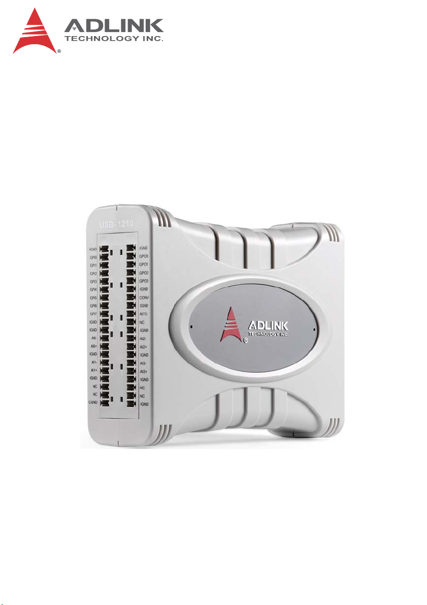
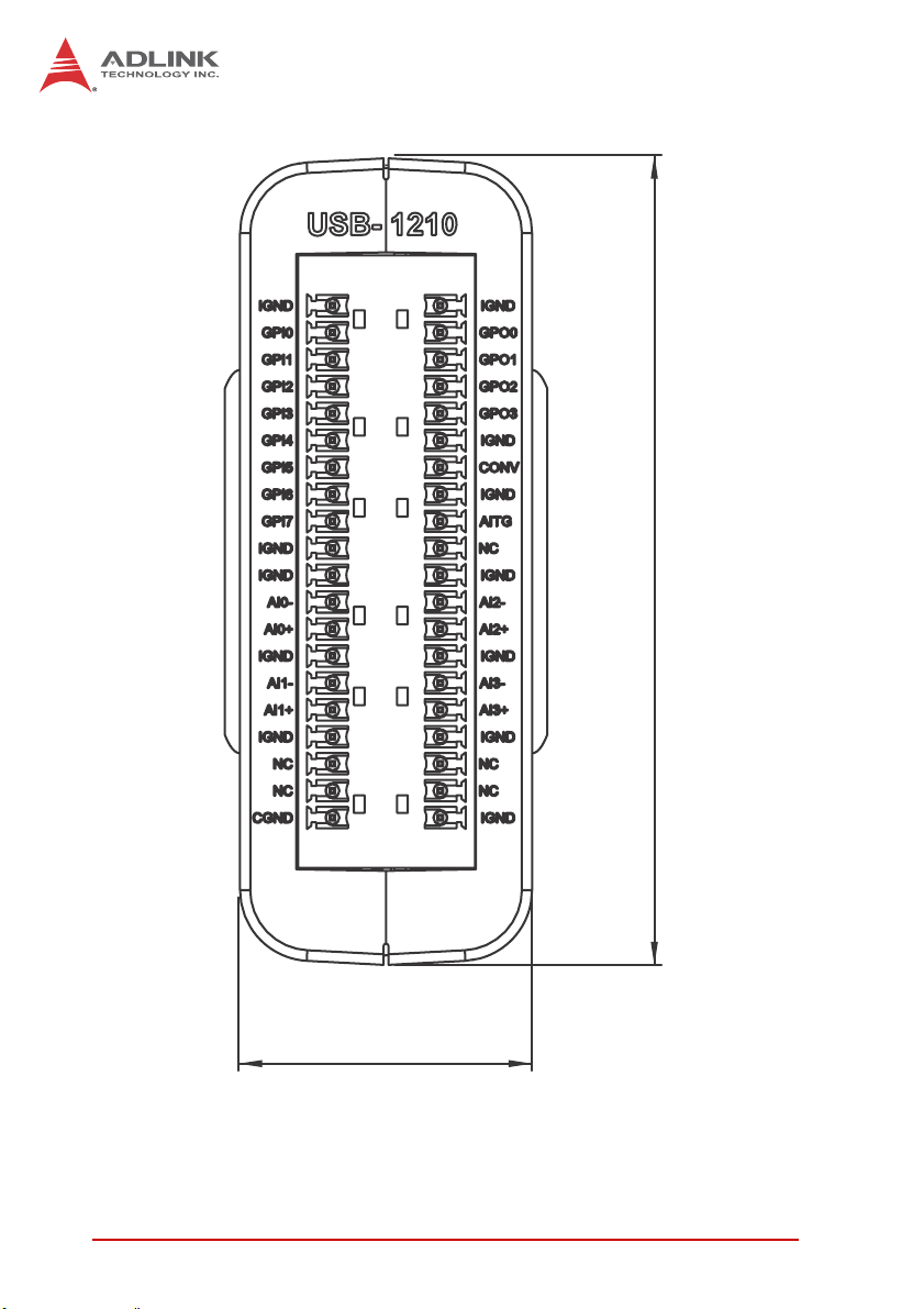
1.6 Connector Pin Assignment
The USB-1210 module is equipped with 40-pin removable
screw-down terminal connectors, with pin assignment as shown.
Pin Pin
IGND 20 40 IGND
GPI0 19 39 GPO0
GPI1 18 38 GPO1
GPI2 17 37 GPO2
GPI3 16 36 GPO3
GPI4 15 35 IGND
GPI5 14 34 CONV
GPI6 13 33 IGND
GPI7 12 32 AITG
IGND 11 31 NC
IGND 10 30 IGND
AI0- 9 29 AI2-
AI0+ 8 28 AI2+
IGND 7 27 IGND
AI1- 6 26 AI3-
AI1+ 5 25 AI3+
IGND 4 24 IGND
NC 3 23 NC
NC 2 22 NC
CGND 1 21 IGND
Table 1-1: USB-1210 Pin Assignment
1.6.1 Connector Signal Description
Signal Reference I/O Description
IGND N/A None Isolated ground for AI and DI/O
AI+[0 to 3]
AI-[0 to 3]
Introduction 11
IGND I Differential Input for channels 0 to 3
Page 22

Signal Reference I/O Description
CGND N/A None Chassis ground
Function Input <0..7>
GPI<0..7> IGND I
GPO<0..3> IGND O
CONV IGND I External A/D conversion clock
AITG IGND I Digital trigger for analog input
NC NC NC No connection
Table 1-2: CN1/CN2 I/O Signal Description
(see Section 3.1.5: Programmable
Function I/O)
Function Output <0..3>
(see Section 3.1.5: Programmable
Function I/O)
1.7 Analog Input Signal Connection
The USB-1210 provides 4 truly differential analog input channels.
These four channels are simultaneous-sampling and support up to
2MS/s per channel. The analog signal can be converted to a digital value by the A/D converter. To avoid ground loops and obtain
more accurate measurement from the A/D conversion, it is important to understand the type of signal source and how to connect
the signal in differential mode.
Signal Source Types
Floating
A floating signal source is not connected in any way to the
existing ground system. A device with an isolated output is a
floating signal source. This includes optical isolator outputs,
transformer outputs, and thermocouples.
Ground-Referenced
A ground-referenced signal is connected in some way to the
existing ground system. That is, the signal source is already
connected to a common ground point with respect to the
USB-1210, assuming that the computer is connected to the
same power system. Non-isolated outputs of instruments and
12 Introduction
Page 23

devices that plug into the existing power systems are
A
A
x
A
A
ground-referenced signal sources.
Input Configurations
Differential Input Mode
Differential input mode provides positive signal and negative
signal inputs that respond to signal voltage difference between
them, as shown. If the signal source is ground-referenced, differential mode can be used for noise rejection for improvement
over single-ended mode.
Ground
referenced
signal source
Common-mode
noise & Ground
potential
Figure 1-10: GRND-Referenced Source w/ DIFF Input
= 0, ..., 3
Vcm
Input multiplexer
IxH
IxL
IGND
Instrumentation amplifier
+
-
To A/D
converter
-
USB-1210
Connection of a floating signal source to the USB-1210 module
in differential input mode is further shown. For floating signal
sources, the negative side of the signal should be connected to
the AIGND, with less noise coupled into the signal connections
than in single-end mode.
IxH
IxL
Input Multiplexer
+
-
IGND
Instrumentation
Amplifier
To A/D
Converter
-
x = 0, ..., 3
Floating
Signal
Source
Figure 1-11: Floating Source w/ DIFF Input
Introduction 13
Page 24

1.8 Software Support
ADLINK provides comprehensive software drivers and packages
to suit various user approaches to system building. In addition to
programming libraries, such as DLLs, for most Windows-based
systems, ADLINK also provides drivers for other application environments such as LabVIEW
are included in the ADLINK All-in-One CD.
Be sure to install the driver & utility before using the USB-1210
module.
®
and MATLAB®. All software options
1.9 Driver Support for Windows
UD-DASK
UD-DASK is composed of advanced 32/64-bit kernel drivers and
SDK for customized DAQ application development. USB-DASK
enables you to perform detailed operations and achieve superior
performance and reliability from your data acquisition system.
DASK kernel drivers now support Windows 7/8 OS.
DAQPilot
DAQPilot is a driver and SDK utility providing control and configuration capabilities for ADLINK USB DAQ devices in LabVIEW®.
You can download and install DAQPilot at:
http://www.adlinktech.com/TM/DAQPilot.html.
1.10 Utilities for Windows
U-Test
U-Test is a free and ready-to-use utility which can assist instant
testing and operation of all ADLINK USB DAQ series functions
with no programming. In addition to providing data collection and
monitoring functions, U-Test also supports basic FFT analysis and
provides direct control of analog output and digital I/O with a
user-friendly interface.
You can download and install U-Test at: http://www.adlinktech.com/
14 Introduction
Page 25

2 Getting Started
2.1 Unpacking Checklist
Before unpacking, check the shipping carton for any damage. If
the shipping carton and/or contents are damaged, inform your
dealer immediately. Retain the shipping carton and packing
materials for inspection. Obtain authorization from your dealer
before returning any product to ADLINK. Ensure that the following items are included in the package.
X USB-1210 module
X Stand
X Two removable screw terminals
X USB cable (2-meter length)
X Rail mount kit
X ADLINK All-in-One CD
X User’s manual
2.2 Attaching the Module Stand
The multi-function USB-1210 stand is compatible with desk, rail, or
wall mounting. To fix the module in the stand, slide the module
body into the stand until a click is heard. To remove the module
from the stand, twist the bottom of the stand in a back-and forth
motion and separate from the module.
USB-1210
Getting Started 15
Page 26

2.3 Rail Mounting
The multi-function stand can be mounted on the DIN rail using the
rail-mount kit as shown.
Figure 2-1: Rail Mount Kit
Figure 2-2: Module Pre-Rail Mounting
16 Getting Started
Page 27

Figure 2-3: Module Rail-Mounted
2.4 Wall Mounting
USB-1210
The multi-function stand can be fixed to a wall using four flush
head screws as shown. The four screw holes should be
approximately 3.4 mm in diameter.
20.4
13.0
Figure 2-4: Wall Mount Holes
Getting Started 17
Page 28

Figure 2-5: Module with Wall Mount Apparatus
2.5 Installing the USB-1210 Module
The appropriate driver must be installed before you can connect the USB DAQ to your computer system. Refer to
WARNING:
2.5.1 Connecting the USB-1210 Module
Section 1.9: Driver Support for Windows for driver support
information.
1. Turn on your computer.
2. Connect the USB-1210 module to one USB 2.0 port on
your computer using the included USB cable.
3. The first time the USB-1210 module is connected, a New
Hardware message appears. It will take around 6 seconds to load the firmware. When loading is complete, the
LED indicator on the rear of the USB DAQ module
changes from amber to green and the New Hardware
message closes.
4. The USB-1210 module can now be located in the hardware Device Manager, listed as ADLINK USBDAQ 1210
Device as shown.
18 Getting Started
Page 29

USB-1210
Figure 2-6: USB-1210 module in Windows Device Manager
If the USB-1210 module cannot be detected, the power provided
by the USB port may be insufficient. The USB-1210 module is
exclusively powered by the USB port and requires 460 mA @ 5 V.
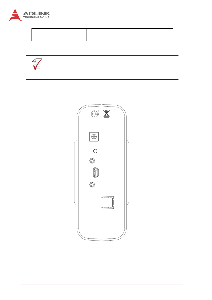
2.5.2 Device ID
A rotary control on the rear of the module (as shown) controls
device ID setting and can be set from 1 to 8. The device ID allows
dedicated control of the USB-1210 module irrespective of the connected USB port. When more than one USB module of the same
Getting Started 19
Page 30

type is connected, each must be set to a different ID to avoid conflicts and errors in operation.
Figure 2-7: Device ID Selection Control
2.5.3 Hardware Configuration
All remaining hardware configurations are software
programmable, including sampling/update rate, input/output
channel, input range, and others. Please see the UD-DASK
Function Reference manual for details.
20 Getting Started
Page 31

3 Operation & Calibration
Operation of the USB-1210 is described here to assist in
configuration and programming of the module. Functions
described include A/D conversion, programmable function I/O,
and others
3.1 Operation
3.1.1 Signal Function
The USB-1210 provides 4 truly differential and
simultaneous-sampling analog input channels of 16-bit A/D input.
Each A/D input channel is connected to one ADC (LT LTC2380 or
equivalent). The ADC controller and all timing control logics are
implemented by the FPGA. The USB-1210 utilizes calibration
circuits to provide high performance and low-temperature drift
signal acquisition. Calibration data is saved in the EEPROM.
80 MHz
DIO
CPLD SPI
BUS
ADC BUS
OSC
GPTC
Configuration
AI Calibration CTRL
8051 Core
Function
FPGA
Configuration
ADC Control
Trigger Control
Data Processing
FIFO
DDR3
EEPROM
A
D
A
D
3.3V, 1.2V
Supply
/
D
A
T
24 MHz
XTAL
Cypress
CY7C68013A
8051 Core
12/24/48MHz
3.3V Supply
Power
Circuit
Isolation Moat
DIO
Trigger
And
AI Configuration
ADC SPI
Trigger
DI
DO
DIO and Trigger
66 MHz
OSC
AI Configuration
CPLD
ADC SPI BUS
Isolated
Isolated
CPLD SPI
BUS
Isolated
ADC BUS
Isolator
Circuit
Isolator
Circuit
Isolator
Circuit
40 Pin Board to Board Conn x2
Isolated 3.3V
Supply
Isolated +13V, -13V
Supply
Isolation
Power
Circuit
USB-1210
USB Bus
PXIe_DSTARCp/n
PCIe Gen1
x4
USB BUS
+5V Supply
USB Interface
Figure 3-1: Carrier Board Functional Block Diagram
Operation & Calibration 21
Page 32

AI CH0+
AI CH0-
AI CH1+
AI CH1-
AI CH2+
AI CH2-
AI CH3+
AI CH3-
Signal
Protection
IO Connector
Signal
Protection
DC path/
Calibration Source
SW
Calibration
Mux and
Reference Src
DC path/
Calibration Source
SW
PGA
PGA
2nd-order
LPF
2nd-order
LPF
1st CH
Four channels
ADC
4th CH
SDO_CH0
BUSY_CH0
SDO_CH1
BUSY_CH1
SDO_CH2
BUSY_CH2
SDO_CH3
BUSY_CH3
SCK
40 Pin Board to Board Conn x2
DI CH[7..0]
DO CH[3..0]
AI TRIGGER
DO
Trigger
DI
Trigger
DIO
And
Figure 3-2: Daughter Board Functional Block Diagram
3.1.2 A/D Conversion
When using an A/D converter, the properties of the signal to be
measured must be considered and a channel and connection of
signals to the module selected. Please see Section 1.7: Analog
Input Signal Connection. As well, A/D signal configuration,
including channel, gain, and signal type must be defined and set.
A/D acquisition is initiated by a predefined trigger source. Data
acquisition will commence once a trigger condition is matched.
After A/D conversion, A/D data is buffered in a data FIFO for
transfer into system memory for further processing.
22 Operation & Calibration
Page 33

USB-1210
Analog Input Circuitry
AI CHx_P
Signal Input
AI CHx_N
Signal Input
2 MHz
Path_DC
Calibration SRC
Signal Protection
Path Selection
MUX
MUX
PGA
With
x1 or x4
PGA
MUX
2nd order
With level shift
REF
IC
x
2
LPF
x1/2
x1
Figure 3-3: Analog Input
Clock
Buffer
CLK
SW
Buffer
A
D
C
O
N
V
_
C
H
0
ADC
AI Data Format
The acquired 16-bit A/D data is 2’s complement coded data format. Valid input ranges and ideal transfer characteristics are
shown.
ADCONV_CHn
Description Bipolar Analog Input Range Digital Code
Full-scale range ±10 V ±2 V N/A
Least significant bit 305.2 µV 61.03 µV N/A
FSR-1LSB 9.999695V 1.999938V 7FFF
Midscale +1LSB 305.2 µV 61.03 µV 0001
Midscale 0 V 0 V 0000
Midscale –1LSB -305.2 µV -61.03 µV FFFF
-FSR -10 V -2 V 8000
Table 3-1: Bipolar Analog Input Range and Output Digital Code
Operation & Calibration 23
Page 34

Software Conversion with Polling Data Transfer Acquisition Mode (Software Polling)
Generally the most convenient way to acquire a single A/D data
sample, the A/D converter starts a conversion when the dedicated
software command is executed. The software then polls the
conversion status and reads back the A/D data when it is
available.
This method is indicated when there is a need to process A/D data
in real time or instant closed-loop control. In this mode, the timing
of the A/D conversion is fully controlled by the software.
The A/D conversion rate is determined by the software timer
and may not be precise.
WARNING:
Continuous Acquisition Mode
Continuous A/D Conversion Clock Source
When the onboard ADC receives a conversion clock signal,
A/D conversion is triggered. The USB-1210 conversion clock
may originate with the internal hardware timer or externally via
CONV (external A/D conversion clock) pin. While the conversion clock source can be chosen by setting AI source configuration, if precision acquisition is required, use of the internal
hardware timer is recommended.
Sampling Rate Control with Internal Hardware Timer
This mode is recommended if a fixed and precise A/D sampling
rate is required.The period between conversions of individual
channels can be accurately programmed. ADC sampling rate is
determined by:
Sampling Rate = 2M/ScanIntrv Where ScanIntrv is scan
interval counter, value can be 1, 2, 3, 4… 232 - 1
24 Operation & Calibration
Page 35

Trigger
TIMEBASE
ScanIntrv = 1
USB-1210
D2
D1
D4
D3
D6
D5
D8
D7
D10
D9
DATA
ScanIntrv = 2
ScanIntrv = 3
Acquisition
In Progress
D1
D1
Acquisition begins following this clock edge
D2 D3 D4 D5 D6
D2 D3 D4
Figure 3-4: Configuring Different Sampling Rates
Sampling Rate Control with External Conversion Strobe Clock
The A/D conversion clock can be provided by external strobe
clock via CONV pin. The valid frequency of external clock is from
DC to 2 MHz and the minimum pulse width is 225ns.
Analog Input Triggering
The USB-1210 supports flexible trigger sources for analog input
functionality. The trigger source can originate with software command, external analog, or external digital signal in continuous analog input mode. Users can configure the trigger source and trigger
mode by software.
3.1.3 Trigger Sources
Software Triggering
This trigger mode requires no external trigger source. The trigger
asserts immediately following execution of the specified function
calls to begin the operation.
External Analog Triggering
The analog multiplexer can select one input channel as the analog
trigger source. That is, one of 4 input channels in differential mode
can be selected as the analog trigger source. An external analog
Operation & Calibration 25
Page 36

trigger occurs when the analog trigger signal crosses above
(above high) or below (below low) the pre-defined voltage level.
The range of trigger level is the full-scale range of the selected
input channel and the resolution is 16-bit.
Below-Low Analog Triggering
In below-low analog triggering, as shown, the trigger signal is
generated when the input analog signal is less than the
Low_Threshold voltage. High_Threshold setting is not used in
this triggering situation.
Figure 3-5: Below-Low Analog Triggering
Above-High Analog Triggering
In above-high analog triggering, as shown, the trigger signal is
generated when the input analog signal exceeds the
High_Threshold voltage. Low_Threshold setting is not used in
this triggering situation
26 Operation & Calibration
Page 37

USB-1210
Figure 3-6: Above-High Analog Triggering
External Digital Triggering
An external digital trigger occurs when a rising or falling edge is
detected on the digital signal connected to the AITG (analog input
trigger) pin. Trigger polarity can be programmed using ADLINK
software drivers.
Signal level of the external digital trigger signals should be
LVTTL-compatible, with a minimum pulse of 20ns.
WARNING:
Positi ve-edge (rising)
t r i gger event occu r s
Negati ve-edge (f all ing)
t r i gger event occ ur s
Figure 3-7: Digital Triggering
3.1.4 Trigger Modes
Analog input supports post, pre, middle, delay, gate, post trigger
with retrigger, and delay trigger with retrigger modes.
Operation & Calibration 27
Page 38

Post-Trigger Acquisition Mode (no retriggering)
Post-trigger acquisition is indicated when data is to be collected
after the trigger event, as shown..
Trigger
ƔOperation
initiates
ƔTrigger event occurs
ƔAcquisition begins
N samplesData
ƔAcquisition stops
ƔData transfer to system commences
Figure 3-8: Post Trigger without Retriggering
Delayed-Trigger Acquisition Mode (no retriggering)
Delay-trigger acquisition is indicated when the data collection is to
be delayed following the trigger event, as shown. Delay duration is
specified by a 32-bit counter value, whereby maximum delay is the
period of TIMEBASE X (2
the timebase.
32
- 1), and minimum delay the period of
Time
ƔOperation initiates
Trigger
Data
ƔTrigger event occurs
Delay Time
ƔAcquisition begins
N samples
ƔAcquisition stops
ƔData transfer to system begins
Time
Figure 3-9: Delayed Trigger
Middle Trigger Mode
Middle-trigger acquisition mode is indicated when data is to be collected before and after the trigger event. The amount of stored
data before and after trigger event can be set individually (M and
N samples), as shown.
28 Operation & Calibration
Page 39

USB-1210
Trigger
Data
ƔOperation initiates
ƔAcquisition initiates
ƔTrigger event occurs
ƔAcquisition stops
ƔData transfer to system begins
N samplesM samples
Figure 3-10: Middle Trigger
Pre-Trigger Mode
Pre-trigger acquisition is indicated when data is to be collected
before the trigger event. Acquisition commences once specified
function calls are executed to begin the pre-trigger operation, and
stops when the trigger event occurs. If the trigger event occurs
after the specified amount of data has been acquired, the system
stores only data preceding the trigger event by a specified
amount, as shown.
ƔTrigger Event Occurs
ƔAcquisition stops
ƔData transfer to system begins
Trigger
Data
ƔOperation initiates
ƔAcquisition initiates
N samples
Time
Time
This data is
discarded
Only the N acquired
samples are
returned to system
Figure 3-11: Pre-Trigger
Post-Trigger or Delayed-Trigger Acquisition Mode with Retriggering
Post-trigger or Delayed-Trigger acquisition with re-trigger function
is indicated when data is to be collected after several trigger
events. An example is shown, in which N samples of data are
Operation & Calibration 29
Page 40

acquired after the first trigger signal, after which the USB-1210
awaits the next re-trigger signal (re-trigger signals occurring
before the N samples are completed will be ignored). When the
re-trigger signal occurs, another N samples are performed. The
process repeats until the specified number of re-trigger signals are
detected.
ƔOperation initiates
Trigger
Data
ƔTrigger event occurs
ƔAcquisition initiates
N samples N samples N samples
Figure 3-12: Post Trigger with Retriggering
Gated Trigger
Gated-trigger acquisition is indicated in applications where you
want to collect data when trigger events are set to level high/low,
and hold acquisition when trigger events are set to the opposite
level.
As shown, after the operation starts, the first scan of data is immediately acquired when the trigger signal is deasserted and paused
when the trigger signal is asserted.
The remaining A/D conversions are not performed until the trigger
signal is deasserted again. The process repeats until the specified
amount of data is acquired.
ƔAcquisition begins
ƔAcquisition stops
Time
ƔOperation initiates
Trigger
(Active High)
Data
ƔAcquisition begins ƔAcquisition stops
ƔAcquisition begins
Time
Figure 3-13: Gated Trigger
30 Operation & Calibration
Page 41

USB-1210
3.1.5 Programmable Function I/O
The USB-1210 supports powerful programmable I/O function provided by an FPGA chip, configurable as LVTTL DI/DO, 32-bit
timer/counters, and PWM output. These signals are single-ended
and 5 V LVTTL-compliant.
LVTTL DI/DO
Programmable function I/O can be used as static LVTTL-compliant 8-CH digital input and 4-CH digital output. You can read/write
these I/O lines by software polling, with sample and update rate
fully controlled by software timing.
Pin# Pin#
IGND 20 40 IGND
GPI0 19 39 GPO0
GPI1 18 38 GPO1
GPI2 17 37 GPO2
GPI3 16 36 GPO3
GPI4 15 35 IGND
GPI5 14 34 N/C*
GPI6 13 33 N/C*
GPI7 12 32 N/C*
IGND 11 31 N/C*
*Not used in DI/O
Table 3-2: Pin Definition of LVTTL Digital I/O
General Purpose Timer/Counter
The USB-1210 is equipped with two general purpose timer/counter sets featuring:
X Count up/down controllable by hardware or software
X Programmable counter clock source (internal clock up to 80
MHz, external clock up to 10 MHz)
Operation & Calibration 31
Page 42

X Programmable gate selection (hardware or software con-
trol)
X Programmable input and output signal polarities (high active
or low active)
X Initial Count loaded from a software application
X Current count value readable by software without affecting
circuit operation.
Pin Pin
IGND 20 40 IGND
GPTC_CLK 19 39 GPTC_OUT0
GPTC_UD0 18 38 GPTC_OUT1
GPTC_GATE0 17 37 GPTC_OUT2
GPTC_AUX0 16 36 GPTC_OUT3
GPTC_CLK2 15 35 IGND
GPTC_UD2 14 34 N/C*
GPTC_GATE2 13 33 N/C*
GPTC_AUX2 12 32 N/C*
IGND 11 31 N/C*
*Not used in GPTC
Table 3-3: Timer/Counter Pin Definition
3.1.6 Basic Timer/Counter Function
Each timer/counter has three inputs that can be controlled via
hardware or software. They are clock input (GPTC_CLK), gate
input (GPTC_GATE), and up/down control input (GPTC_UD). The
GPTC_CLK input provides a clock source input to the timer/counter. Active edges on the GPTC_CLK input increment or decrement
the counter. The GPTC_UD input directs the counter to count up
or down (high: count up; low: count down), while the GPTC_GATE
input is a control signal acting as a counter enable or counter trigger signal in different applications. The GPTC_OUT then generates a pulse signal based on the timer/counter mode set.
32 Operation & Calibration
Page 43

USB-1210
All input/output signal polarities can be programmed by software
application. For brevity, all GPTC_CLK, GPTC_GATE, and
GPTC_OUT in the following illustrations are assumed to be active
high or rising-edge triggered.
3.1.7 General Purpose Timer/Counter Modes
Ten programmable timer/counter modes are available. All modes
initialize following a software-start signal set by the software. The
GPTC software reset initializes the status of the counter and
reloads the initial value to the counter. The operation remains
halted until software start is executed again. Operations under different modes are described as follows.
Mode 1: Simple Gated-Event Counting
In this mode, the counter calculates the number of pulses on the
GPTC_CLK after a software start. Initial count can be loaded from
the software application. Current count value can be read back by
software any time with no influence on calculation. GPTC_GATE
enables/disables calculation. When GPTC_GATE is inactive, the
counter halts the current count value. Operation in which initial
count = 5, countdown mode is shown.
Software start
Gate
CLK
Count value
Figure 3-14: Mode 1-Simple Gated-Event Calculation
55 432110 ffff
Mode 2: Single Period Measurement
The counter calculates the period of the signal on GPTC_GATE in
terms of GPTC_CLK. The initial count can be loaded from the software application. After software start, the counter calculates the
number of active edges on GPTC_CLK between two active edges
Operation & Calibration 33
Page 44

of GPTC_GATE. After the completion of the period interval on
GPTC_GATE, GPTC_OUT outputs high and then current count
value can be read by the software application. Operation in which
initial count = 0, count-up mode is shown.
Software start
Gate
CLK
Count value
Figure 3-15: Mode 2-Single Period Measurement
00 1234555
Mode 3: Single Pulse-Width Measurement
The counter calculates the pulse-width of the signal on
GPTC_GATE in terms of GPTC_CLK. Initial count can be loaded
from the software application. After software start, the counter calculates the number of active edges on GPTC_CLK when
GPTC_GATE is in its active state.
After the completion of the pulse-width interval on GPTC_GATE,
GPTC_OUT outputs high and current count value can be read by
the software application. Operation in which initial count = 0,
count-up mode is shown.
Software start
Gate
CLK
Count value
34 Operation & Calibration
00 1234555
Page 45

USB-1210
Figure 3-16: Mode 3-Single Pulse-Width Measurement
Mode 4: Single-Gated Pulse Generation
This mode generates a single pulse with programmable delay and
programmable pulse-width following software start. The two programmable parameters can be specified in terms of periods of the
GPTC_CLK input by the software application. GPTC_GATE
enables/disables calculation. When GPTC_GATE is inactive, the
counter halts the current count value. Generation of a single pulse
with a pulse delay of two and a pulse-width of four is shown.
Software start
Gate
CLK
Count value
OUT
Figure 3-17: Mode 4-Single-Gated Pulse
22 1032210
Mode 5: Single-Triggered Pulse
This mode generates a single pulse with programmable delay and
programmable pulse-width following an active GPTC_GATE edge.
These programmable parameters can be specified in terms of
periods of the GPTC_CLK input. When the first GPTC_GATE
edge triggers the single pulse, GPTC_GATE has no effect until
software start is executed again. Generation of a single pulse with
a pulse delay of two and a pulse-width of four is shown.
Operation & Calibration 35
Page 46

Gate
CLK
Software start
Count value
22103210
OUT
Figure 3-18: Mode 5-Single-Triggered Pulse
Mode 6: Re-Triggered Single Pulse Generation
This mode is similar to Mode 5 except that the counter generates
a pulse following every active edge of GPTC_GATE. After software start, every active GPTC_GATE edge triggers a single pulse
with programmable delay and pulse width. Any GPTC_GATE triggers that occur when the prior pulse is not completed are ignored.
Generation of two pulses with a pulse delay of two and a pulse
width of four is shown.
S o f t w a r e s t a r t
G a t e
C L K
C o u n t v a l u e
O U T
22 1032102
Figure 3-19: Mode 6-Re-Triggered Single Pulse
I g n o r e d
210
32102
2
Mode 7: Single-Triggered Continuous Pulse Generation
This mode is similar to Mode 5 except that the counter generates
continuous periodic pulses with programmable pulse interval and
pulse-width following the first active edge of GPTC_GATE. When
the first GPTC_GATE edge triggers the counter, GPTC_GATE
has no effect until software start is executed again. Generation of
two pulses with a pulse delay of four and a pulse-width of three is
shown.
36 Operation & Calibration
Page 47

USB-1210
S o f t w a r e s t a r t
G a t e
C L K
C o u n t v a l u e
O U T
44 4321021
0321021
032
Figure 3-20: Mode 7-Single-Triggered Continuous Pulse
Mode 8: Continuous Gated Pulse Generation
This mode generates periodic pulses with programmable pulse
interval and pulse-width following software start. GPTC_GATE
enables/disables calculation. When GPTC_GATE is inactive, the
counter halts the current count value. Generation of two pulses
with a pulse delay of four and a pulse-width of three is shown.
S o f t w a r e s t a r t
G a t e
C L K
C o u n t v a l u e
O U T
44 3321021
0321021
103
Figure 3-21: Mode 8-Continuous Gated Pulse
Mode 9: Edge Separation Measurement
Measures the time differentiation between two different pulse signals. The first pulse signal is connected to GPTC_GATE and the
second signal is connected to GPTC_AUX. Clocks that pass
between the rising edge signal of two different pulses through the
80 MHz internal clock or external clock are calculated. You can
calculate the time period via the known clock frequency. The max-
Operation & Calibration 37
Page 48

imum counting width is 32-bit. Decrease of the counter value in
Edge Separation Measurement mode is shown.
S o f t w a r e s t a r t
G a t e
A U X
C L K
C o u n t v a l u e
1313 12 11 9 8 7 6
10
5432111111
Figure 3-22: Mode 9-Edge Separation Measurement
Mode 10: PWM Output
The USB-1210 timer/counter can also simulate a PWM (Pulse
Width Modulation) output. The PWM starts to generate output following a GPTC_GATE edge trigger or being activated/inactivated
by the GPTC_GATE high/low logic control. By setting a varying
amount of Pulse_initial_cnt and Pulse_length_cnt, varying pulse
frequencies (Fpwm) and duty cycles (Dutypwm) can be obtained.
PWM output is shown.
Software Start
Gate
PWMOUT
TIMEBASE
Pulse_Initial_cnt= 0x7
Pulse_Length_cnt= 0xB
Figure 3-23: Mode 10-PWM Output Following Trigger
Software Start
Gate
PWMOUT
TIMEBASE
Pulse_Initial_cnt= 0x7
Pulse_Length_cnt= 0xB
Figure 3-24: Mode 10-PWM Output Following GATE Control
Calculation of the PWM frequency and duty cycle is as follows.
38 Operation & Calibration
Page 49

USB-1210
F
F
PWM
Duty
=
PWM
=
Time base
+
cntlengthPulsecntinitialPulse
____
cntlengthPulse
__
cntlengthPulsecntinitialPulse
+
____
3.1.8 Isolation
The USB-1210 provides 500VDC isolation capability to protect
against hazardous voltage caused by erroneous signal connection
or signal levels to be measured exceeding expectation. The isolation circuit can also reduce the ground-loop noise.
DDR3
ADC
DIO
CPLD
FPGA
Isolator
Power
Isolation
Power
USB
Controller
USB BUS
+5V
Supply
USB-1210
Figure 3-25: Isolation
3.2 Calibration
3.2.1 Loading Calibration Constants
The USB-1210 is factory-calibrated before shipment. The associated calibration constants of the TrimDACs firmware are written to
the onboard EEPROM. TrimDACs firmware is the algorithm in the
Operation & Calibration 39
USB Interface
Page 50

FPGA. Loading calibration constants entails loading the values of
TrimDACs firmware stored in the onboard EEPROM.
Dedicated space for storing calibration constants is provided in the
EEPROM. In addition to the bank of factory calibration constants,
there is one user-utilization bank, allowing loading of the TrimDACs firmware values either from the original factory calibration or
a subsequently-performed calibration.
The default calibration constants are loaded from the user-utilization bank and are the same as those in the factory calibration bank
if no auto-calibration is performed.
Since measurement and output errors may vary depending on
time and temperature, it is recommended that you calibrate the
USB-1210 module in your existing testing environment, as follows.
3.2.2 Auto-Calibration
USB-1210 auto-calibration utility measures and corrects almost all
calibration errors with no external signal connections, reference
voltage, or measurement devices. The USB-1210 provides
onboard calibration reference to ensure the accuracy of auto-calibration. The reference voltage is measured in the production line
by a digital potentiometer and compensated in the software. The
calibration constant is stored after this measurement.
3.2.3 Saving Calibration Constants
Factory-calibrated constants are permanently stored in a bank of
the onboard EEPROM and cannot be modified. When the device
is recalibrated, the software stores the new constants in a
user-configurable section of the EEPROM. To restore original factory calibration settings, the software can copy the factory-calibrated constants to the user-configurable section of the EEPROM.
When auto-calibration is complete, the new calibration constants
can be saved to the user-configurable banks in the EEPROM.
The USB-1210 should be warmed up for at least 15 minutes
before initiating auto-calibration
NOTE:
NOTE:
40 Operation & Calibration
Page 51

USB-1210
Important Safety Instructions
For user safety, please read and follow all instructions,
WARNINGS, CAUTIONS, and NOTES marked in this manual
and on the associated equipment before handling/operating the
equipment.
X Read these safety instructions carefully.
X Keep this user’s manual for future reference.
X Read the specifications section of this manual for detailed
information on the operating environment of this equipment.
X When installing/mounting or uninstalling/removing
equipment:
Z Turn off power and unplug any power cords/cables.
X To avoid electrical shock and/or damage to equipment:
Z Keep equipment away from water or liquid sources;
Z Keep equipment away from high heat or high humidity;
Z Keep equipment properly ventilated (do not block or
cover ventilation openings);
Z Make sure to use recommended voltage and power
source settings;
Z Always install and operate equipment near an easily
accessible electrical socket-outlet;
Z Secure the power cord (do not place any object on/over
the power cord);
Z Only install/attach and operate equipment on stable
surfaces and/or recommended mountings; and,
Z If the equipment will not be used for long periods of time,
turn off and unplug the equipment from its power source.
Important Safety Instructions 41
Page 52

X Never attempt to fix the equipment. Equipment should only
be serviced by qualified personnel.
A Lithium-type battery may be provided for uninterrupted, backup
or emergency power.
Risk of explosion if battery is replaced with an incorrect type;
please dispose of used batteries appropriately.
WARNING:
X Equipment must be serviced by authorized technicians
when:
Z The power cord or plug is damaged;
Z Liquid has penetrated the equipment;
Z It has been exposed to high humidity/moisture;
Z It is not functioning or does not function according to the
user’s manual;
Z It has been dropped and/or damaged; and/or,
Z It has an obvious sign of breakage.
42 Important Safety Instructions
Page 53

Getting Service
Contact us should you require any service or assistance.
ADLINK Technology, Inc.
Address: 9F, No.166 Jian Yi Road, Zhonghe District
New Taipei City 235, Taiwan
ᄅקؑխࡉ৬ԫሁ 166 ᇆ 9 ᑔ
Tel: +886-2-8226-5877
Fax: +886-2-8226-5717
Email: service@adlinktech.com
Ampro ADLINK Technology, Inc.
Address: 5215 Hellyer Avenue, #110
San Jose, CA 95138, USA
Tel: +1-408-360-0200
Toll Free: +1-800-966-5200 (USA only)
Fax: +1-408-360-0222
Email: info@adlinktech.com
ADLINK Technology (China) Co., Ltd.
Address: Ϟ⍋Ꮦ⌺ϰᮄᓴ∳催⾥ᡔು㢇䏃 300 ো(201203)
300 Fang Chun Rd., Zhangjiang Hi-Tech Park
Pudong New Area, Shanghai, 201203 China
Tel: +86-21-5132-8988
Fax: +86-21-5132-3588
Email: market@adlinktech.com
USB-1210
ADLINK Technology Beijing
Address: ࣫ҀᏖ⍋⎔Ϟഄϰ䏃 1 োⲜ߯ࡼ E ᑻ 801 ᅸ(100085)
Beijing, 100085 China
Tel: +86-10-5885-8666
Fax: +86-10-5885-8626
Email: market@adlinktech.com
ADLINK Technology Shenzhen
Address: ⏅ഇᏖቅ⾥ᡔು催ᮄϗ䘧᭄ᄫᡔᴃು
Tel: +86-755-2643-4858
Fax: +86-755-2664-6353
Email: market@adlinktech.com
LiPPERT ADLINK Technology GmbH
Address: Hans-Thoma-Strasse 11, D-68163
Mannheim, Germany
Tel: +49-621-43214-0
Fax: +49-621 43214-30
Email: emea@adlinktech.com
Rm. 801, Power Creative E, No. 1 Shang Di East Rd.
A1 2 ὐ C (518057)
2F, C Block, Bldg. A1, Cyber-Tech Zone, Gao Xin Ave. Sec. 7
High-Tech Industrial Park S., Shenzhen, 518054 China
Getting Service 43
Page 54

ADLINK Technology, Inc. (French Liaison Office)
Address: 6 allée de Londres, Immeuble Ceylan
91940 Les Ulis, France
Tel: +33 (0) 1 60 12 35 66
Fax: +33 (0) 1 60 12 35 66
Email: france@adlinktech.com
ADLINK Technology Japan Corporation
Address: ͱ101-0045 ᵅҀ䛑ҷ⬄⼲⬄䤯ފ⬎ 3-7-4
Tel: +81-3-4455-3722
Fax: +81-3-5209-6013
Email: japan@adlinktech.com
ADLINK Technology, Inc. (Korean Liaison Office)
Address: 137-881 昢殾柢 昢爎割 昢爎堆嵢 326, 802 (昢爎壟, 微汾瘶捒娯)
Tel: +82-2-2057-0565
Fax: +82-2-2057-0563
Email: korea@adlinktech.com
ADLINK Technology Singapore Pte. Ltd.
Address: 84 Genting Lane #07-02A, Cityneon Design Centre
Tel: +65-6844-2261
Fax: +65-6844-2263
Email: singapore@adlinktech.com
ADLINK Technology Singapore Pte. Ltd. (Indian Liaison Office)
Address: #50-56, First Floor, Spearhead Towers
Malleswaram, Bangalore - 560 055, India
Tel: +91-80-65605817, +91-80-42246107
Fax: +91-80-23464606
Email: india@adlinktech.com
ADLINK Technology, Inc. (Israeli Liaison Office)
Address: 27 Maskit St., Corex Building
PO Box 12777
Herzliya 4673300, Israel
Tel: +972-77-208-0230
Fax: +972-77-208-0230
Email: israel@adlinktech.com
ADLINK Technology, Inc. (UK Liaison Office)
Tel: +44 774 010 59 65
Email: UK@adlinktech.com
⼲⬄ 374 ɛɳ 4F
KANDA374 Bldg. 4F, 3-7-4 Kanda Kajicho,
Chiyoda-ku, Tokyo 101-0045, Japan
802, Mointer B/D, 326 Seocho-daero, Seocho-Gu,
Seoul 137-881, Korea
Singapore 349584
Margosa Main Road (between 16th/17th Cross)
44 Getting Service
 Loading...