

Page 1
Express-IBE2
User’s Manual
Manual Revision: 2.02
Revision Date: December 3, 2014
Part Number: 50-1J045-1020
Page 2

Revision History
Revision Description Date By
2.00 Initial release 2013-08-30 JC
2.01 Correct CPU models, GBE0_MDI0- pin description; remove "Type 6", "USB 3.0", "QNX"; update
Functional Diagram
2.02 Add BIOS beep codes; remove Industrial Temp. SKU 2014-12-03 JC
2014-02-10 JC
Page 2 Express-IBE2
Page 3

Preface
Copyright 2013-14 ADLINK Technology, Inc.
This document contains proprietary information protected by copyright. All rights are reserved. No part of this manual may be reproduced by
any mechanical, electronic, or other means in any form without prior written permission of the manufacturer.
Disclaimer
The information in this document is subject to change without prior notice in order to improve reliability, design, and function and does not
represent a commitment on the part of the manufacturer. In no event will the manufacturer be liable for direct, indirect, special, incidental, or
consequential damages arising out of the use or inability to use the product or documentation, even if advised of the possibility of such
damages.
Environmental Responsibility
ADLINK is committed to fulfilling its social responsibility to global environmental preservation through compliance with the European Union's
Restriction of Hazardous Substances (RoHS) directive and Waste Electrical and Electronic Equipment (WEEE) directive. Environmental
protection is a top priority for ADLINK. We have enforced measures to ensure that our products, manufacturing processes, components, and
raw materials have as little impact on the environment as possible. When products are at their end of life, our customers are encouraged to
dispose of them in accordance with the product disposal and/or recovery programs prescribed by their nation or company.
Trademarks
Product names mentioned herein are used for identification purposes only and may be trademarks and/or registered trademarks of their
respective companies.
Express-IBE2 Page 3
Page 4

Table of Contents
Revision History ............................................................................................................ 2
Preface............................................................................................................................ 3
1. Introduction......................................................................................................... 7
2. Specifications....................................................................................................... 8
2.1. Core System..............................................................................................................................8
2.2. Expansion Busses......................................................................................................................9
2.3. Video.........................................................................................................................................9
2.4. Audio.........................................................................................................................................9
2.5. LAN ...........................................................................................................................................9
2.6. Multi I/O and Storage ...............................................................................................................9
2.7. Super I/O (on carrier using LPC -bus) .................................................................................... 10
2.8. GPIO........................................................................................................................... ............ 10
2.9. Board Controller .................................................................................................................... 10
2.10. Fan Control ............................................................................................................................ 10
2.11. Debug..................................................................................................................................... 10
2.12. Power Specifications ............................................................................................................. 11
2.13. Mechanical and Environmental............................................................................................. 11
2.14. Specification Compliance ...................................................................................................... 11
2.15. Functional Diagram................................................................................................................ 12
2.16. Mechanical Drawing .............................................................................................................. 13
3. COM Express Pinouts and Signal Descriptions ..............................................
3.1. AB / CD Pin Definitions .......................................................................................................... 14
3.2. Signal Description Terminology............................................................................................. 17
3.3. AB Signal Descriptions ........................................................................................................... 18
14
3.3.1. Audio Signals....................................................................................................................................18
3.3.2. Analog VGA ......................................................................................................................................18
3.3.3. LVDS .................................................................................................................................................19
3.3.4. Gigabit Ethernet...............................................................................................................................19
3.3.5. Serial ATA.........................................................................................................................................20
3.3.6. PCI Express.......................................................................................................................................21
3.3.7. Express Card.....................................................................................................................................21
3.3.8. LPC bus.............................................................................................................................................22
3.3.9. USB...................................................................................................................................................22
3.3.10. SPI (BIOS only).............................................................................................................................23
Page 4 Express-IBE2
Page 5

3.3.11. Miscellaneous..............................................................................................................................23
3.3.12. SMBus..........................................................................................................................................24
3.3.13. I2C Bus.........................................................................................................................................24
3.3.14. General Purpose I/O (GPIO) ........................................................................................................24
3.3.15. Power And System Management................................................................................................25
3.3.16. Power and Ground ......................................................................................................................26
3.4. CD Signal Descriptions ........................................................................................................... 27
3.4.1. PATA IDE ..........................................................................................................................................27
3.4.2. PCI ....................................................................................................................................................28
3.4.3. PCI Express Graphics x16 (PEG) or SDVO .........................................................................................30
3.4.4. Module Type Definition ...................................................................................................................32
3.4.5. Power and Ground...........................................................................................................................32
4. Module Configuration ......................................................................................
33
4.1. PCI Express Configuration Switch (SW1) ............................................................................... 33
4.2. PCIe x16-to-two-x8 Adapter Card.......................................................................................... 33
5. System Resources.............................................................................................. 34
5.1. System Memory Map ............................................................................................................ 34
5.2. Direct Memory Access Channels ........................................................................................... 34
5.3. Legacy I/O Map...................................................................................................................... 35
5.4. Interrupt Request (IRQ) Lines................................................................................................ 36
5.5. PCI Configuration Space Map ................................................................................................ 38
5.6. PCI Interrupt Routing Map .................................................................................................... 39
6. BIOS Setup .........................................................................................................40
6.1. Starting the BIOS ................................................................................................................... 40
6.1.1. Setup Menu......................................................................................................................................41
6.1.2. Navigation........................................................................................................................................42
6.2. Main Setup ............................................................................................................................ 45
6.2.1. System Management.......................................................................................................................46
6.3. Advanced Setup..................................................................................................................... 48
6.3.1. ACPI Settings....................................................................................................................................48
6.3.2. Trusted Computing ..........................................................................................................................49
6.3.3. CPU Configuration............................................................................................................................50
6.3.4. SATA Configuration..........................................................................................................................51
6.3.5. Thermal Configuration.....................................................................................................................51
6.3.6. Intel TXT(LT) Configuration ..............................................................................................................53
6.3.7. PCH-FW Configuration.....................................................................................................................53
6.3.8. Intel Anti-Theft Technology Configuration ......................................................................................54
Express-IBE2 Page 5
Page 6

6.3.9. AMT Configuration...........................................................................................................................55
6.3.10. USB Configuration .......................................................................................................................56
6.3.11. W8362DHG Super IO Configuration............................................................................................57
6.3.12. Serial Port Console Redirection...................................................................................................58
6.3.13. CPU PPM Configuration ..............................................................................................................59
6.4. Chipset Setup......................................................................................................................... 60
6.4.1. PCH-IO Configuration.......................................................................................................................60
6.4.2. System Agent (SA) Configuration.....................................................................................................64
6.5. Boot Setup ............................................................................................................................. 70
6.6. Security Setup........................................................................................................................ 71
6.7. Save & Exit Menu................................................................................................................... 72
7. BIOS Checkpoints, Beep Codes........................................................................ 73
7.1. Status Code Ranges ............................................................................................................... 74
7.2. Standard Status Codes........................................................................................................... 74
7.2.1. SEC Status Codes..............................................................................................................................74
7.2.2. SEC Beep Codes................................................................................................................................75
7.2.3. PEI Status Codes...............................................................................................................................75
7.2.4. PEI Beep Codes.................................................................................................................................77
7.2.5. DXE Status Codes .............................................................................................................................77
7.2.6. DXE Beep Codes...............................................................................................................................79
7.2.7. ACPI/ASL Checkpoint .......................................................................................................................80
7.3. OEM-Reserved Checkpoint Ranges ....................................................................................... 80
Safety Instructions ...................................................................................................... 81
Getting Service ............................................................................................................ 82
Page 6 Express-IBE2
Page 7

1. Introduction
The Module Computing Product Segment (MCPS) is pleased to introduce its latest COM Express® Type 2 Module with Intel® Core™ i7/i5/i3
Processor and QM77 Chipset, the Express-IBE2.
The Express-IBE2 is a COM Express® COM.0 R2.1 Type 2 module with a 3rd Generation Intel® Core™ i7/i5/3 processor and support
for error-correcting code (ECC) memory.
Based on the latest Mobile Intel® QM77 Express Chipset, the Express-IBE2 is specifically designed for customers who need a highly
reliable platform and/or continued support for PCI-bus and PATA IDE in a long product life solution.
The Express-IBE2 features the Intel® Core™ i7/i5/i3 processor supporting Intel® Hyper-Threading Technology (up to 4 cores, 8 threads)
and DDR3 dual-channel memory at 1066/1333/1600 MHz with error-correcting code (ECC). Integrated HD Graphics 4000 includes features
such as OpenGL 3.1, DirectX11, Intel® Clear Video HD Technology, Advanced Scheduler 2.0, 1.0, XPDM support, and DirectX Video
Acceleration (DXVA) support for full AVC/VC1/MPEG2 hardware decode. Graphics outputs include VGA, LVDS and SDVO. In addition to
the onboard integrated graphics, a multiplexed PCI Express® x16 Graphics bus is available for discrete graphics expansion or general
purpose x8 or x4 PCI Express® connectivity. The Express-IBE2 features a single onboard Gigabit Ethernet port, four USB eight USB 2.0
ports, two SATA 6 Gb/s ports, two SATA 3 Gb/s ports and one PATA IDE port. Support is provided for SMBus and I
The module is equipped with an SPI AMI EFI BIOS and supports SEMA (Smart Embedded Management Agent). SEMA functionality is
consistent over ADLINK's whole COM product line and provides the following embedded features: BIOS failsafe,
voltage/current/temperature monitoring, power sequence control and monitoring, watchdog control, board info and statistics. SEMA comes
with extensive software and library support for Windows, Linux, and VxWorks.
2
C.
Express-IBE2 Page 7
Page 8

2. Specifications
2.1. Core System
• CPU: 3rd Generation Intel® Core™ Processor, 2-core and 4-core mobile processor with Integrated Graphics, BGA 1023 type
• Intel® Core™ i7-3615QE Quad-Core at 2.3 GHz (3.3/3.1 GHz Turbo), 6MB L3 cache, 45W
• Intel® Core™ i7-3612QE Quad-Core at 2.1 GHz (3.1/2.8 GHz Turbo), 6MB L3 cache, 35W
• Intel® Core™ i7-3555LE Dual-Core at 2.5 GHz (3.2/3.1 GHz Turbo), 4MB L3 cache, 25W
• Intel® Core™ i7-3517UE Dual-Core at 1.7 GHz (2.8/2.6 GHz Turbo), 4MB L3 cache, 17W
• Intel® Core™ i5-3610ME Dual-Core at 2.7 GHz (3.3/3.1 GHz Turbo), 3MB L3 cache, 35W
• Intel® Core™ i3-3120ME Dual-Core at 2.4 GHz, 3MB L3 cache, 35W
• Intel® Core™ i3-3127UE Dual-Core at 1.6 GHz, 3MB L3 cache, 17W
• Intel® Celeron® 1020E Dual-Core at 2.20 GHz, 2MB L3 Cache, 35W
• Intel® Celeron® 1047UE Dual-Core at 1.40 GHz, 2MB L3 Cache, 17W
• Intel® Celeron® 927UE Single-Core at 1.50 GHz, 1MB L3 Cache, 17W
• Cache: 2MB to 16MB LLC cache depending on CPU type
• Memory: dual stacked SO-DIMM socket memory on top
Dual channel DDR3 Memory DDR3 data transfer rates of 1066 MT/s, 1333 MT/s and 1600 MT/s
• Chipset: Mobile Intel® QM77 Express Chipset
• BIOS: AMI EFI with CMOS backup in 16 Mbit SPI BIOS
• Hardware Monitor: Supply voltages and CPU temperature
• Fan Control: on mini connector on module
• Debug Interface: XDP SFF-26 extension for ICE debug
• Management: Intel® AMT 8.0
Page 8 Express-IBE2
Page 9

2.2. Expansion Busses
• PCI Express Gen 3.0 Graphics (PEG) Port x16 supporting up to 8GT/Sec transactions
Configurable as 1 x16 , 2 x8 or 1 x8-lane and 2 x4-lane
• AB Connenctor
PCI Express Gen 2.0 Ports 8 x1 from PCH, 5 x1 free for use
(lane 7 to GbE LAN, lane 6 to PCI bridge, lane 5 to PATA bridge)
Port 0/1/2/3/4 configurable as 5 x1 or 1 x4 and 1 x1
• LPC bus, SPI bus (BIOS only)
• SMBus (system) , I2C (user)
2.3. Video
• Integrated in Processor: Intel® HD Graphics 4000 at 650–1200 MHz (depending on processor)
• Integrated Video: DirectX 11, OpenGL *3.1, OpenCL* 1.1
• Feature Support:
Intel Clear Video HD Technology
Advanced Scheduler 2.0, 1.0, XPDM support
DirectX Video Acceleration (DXVA) support for full AVC/VC1/
MPEG2 hardware decode
Multi Display Support: 3 independent displays
• Display Types
VGA Interface support with 300 MHz DAC Analog monitor support up to QXGA (2048 x 1536)
LVDS Interface Dual channel 18/24-bit LVDS
SDVO (mulitplexed on PEG, selectable in BIOS)
2.4. Audio
• Integrated: Intel® HD Audio integrated in PCH QM77
• Audio Codec: Realtek ALC888/886 on Express-BASE
2.5. LAN
• Integrated: LAN MAC integrated in PCH QM77
• Intel PHY: 82579 Gigabit Ethernet
• Interface: 10/100/1000 GbE connection
2.6. Multi I/O and Storage
• Integrated in PCH QM77
• USB ports: 8 ports USB 2.0 (USB0~7)
• SATA ports: two ports SATA 6Gb/s (SATA0, SATA1), two ports SATA 3 Gb/s (SATA2, SATA3)
• PATA ports: through PCIe to PATA bridge Marvell 88SE6101
Express-IBE2 Page 9
Page 10

2.7. Super I/O (on carrier using LPC -bus)
• Chipset: Winbond W83627HG-AW and W83627DHG-P, without keyboard A20 line
• Parallel Port: LPT1
• Serial Ports: COM1 / COM2 (with console redirection)
2.8. GPIO
• Chipset: NXP PCA9535
• Description: 16-bit I2C-bus and SMBus, low power I/O port with interrupt
• GPO: 4 ports
• GPI: 4 ports with interrupt
2.9. Board Controller
• Type: SEMA BMC
• Functions:
• Power Features
• AT mode control
• ECO mode support (cut 5Vsb during S5) but keep power on RTC clock
• Emergency Shutdown
• Power Status Mointoring and Signalling (LED)
• Current Monitor
• Flat Panel Control
• Support for PWM control on carrier
• Backlight Enable and Vdde inhibit
• General Purpose I2C
• Dual BIOS with Failsave mode
• Watchdog Timer
• Fan Control
• TPM (Trusted Platform Module)
• Chipset: Infineon SLB9635TT1.2
• Type: TPM 1.2
2.10. Fan Control
• Control Source: Temperature Sensor
• Location
• 4-pin Mini connector on module: PWM and TACH 5V based on module
2.11. Debug
• JTAG: SFF connector for XDP to CPU
• LPC header: for mounting POST CODE assembly
Page 10 Express-IBE2
Page 11

2.12. Power Specifications
• Power Modes: AT and ATX mode (AT mode start controlled by ADMT)
• Standard Voltage Input: ATX = 12V±5% / 5Vsb or AT = 12V±5%
• Wide Voltage Input: ATX = 8.5~19V / 5Vsb or AT = 8.5 ~19V
• Power Management: ACPI 3.0 compliant, Smart battery support.
• Power States: supports C1-C6, S0, S1, S4, S3, S5 (Wake on USB S3/S4, WOL S3/S4/S5)
2.13. Mechanical and Environmental
• Standard Operating Temperature: 0 to 60°C
2.14. Specification Compliance
• PICMG COM.0: Rev 2.1 Type 2, basic size 125 x 95
Express-IBE2 Page 11
Page 12
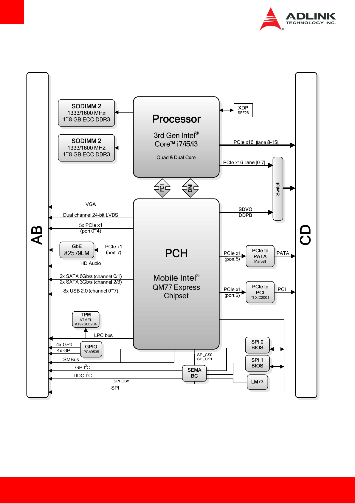
2.15. Functional Diagram
Page 12 Express-IBE2
Page 13
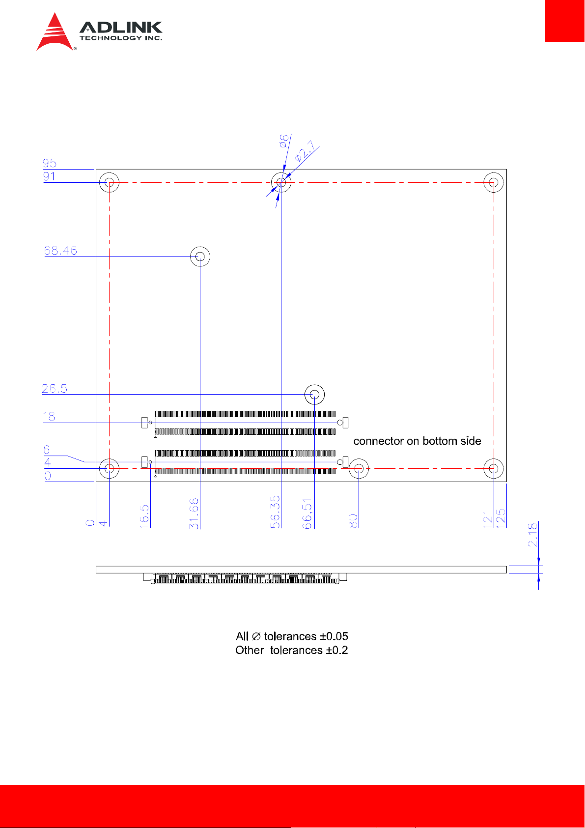
2.16. Mechanical Drawing
Express-IBE2 Page 13
Page 14
3. COM Express Pinouts and Signal Descriptions
The following information is a summary of the most important information regarding pinout and signal description in the official PICMG
COM.0 Rev 2.0 (soon 2.1)
The pinout is described here to emphazise issues that have not been followed in the past. The following description may still contain small
inacuaracies; in case of doubt, the offical design guide of PICMG should be consulted.
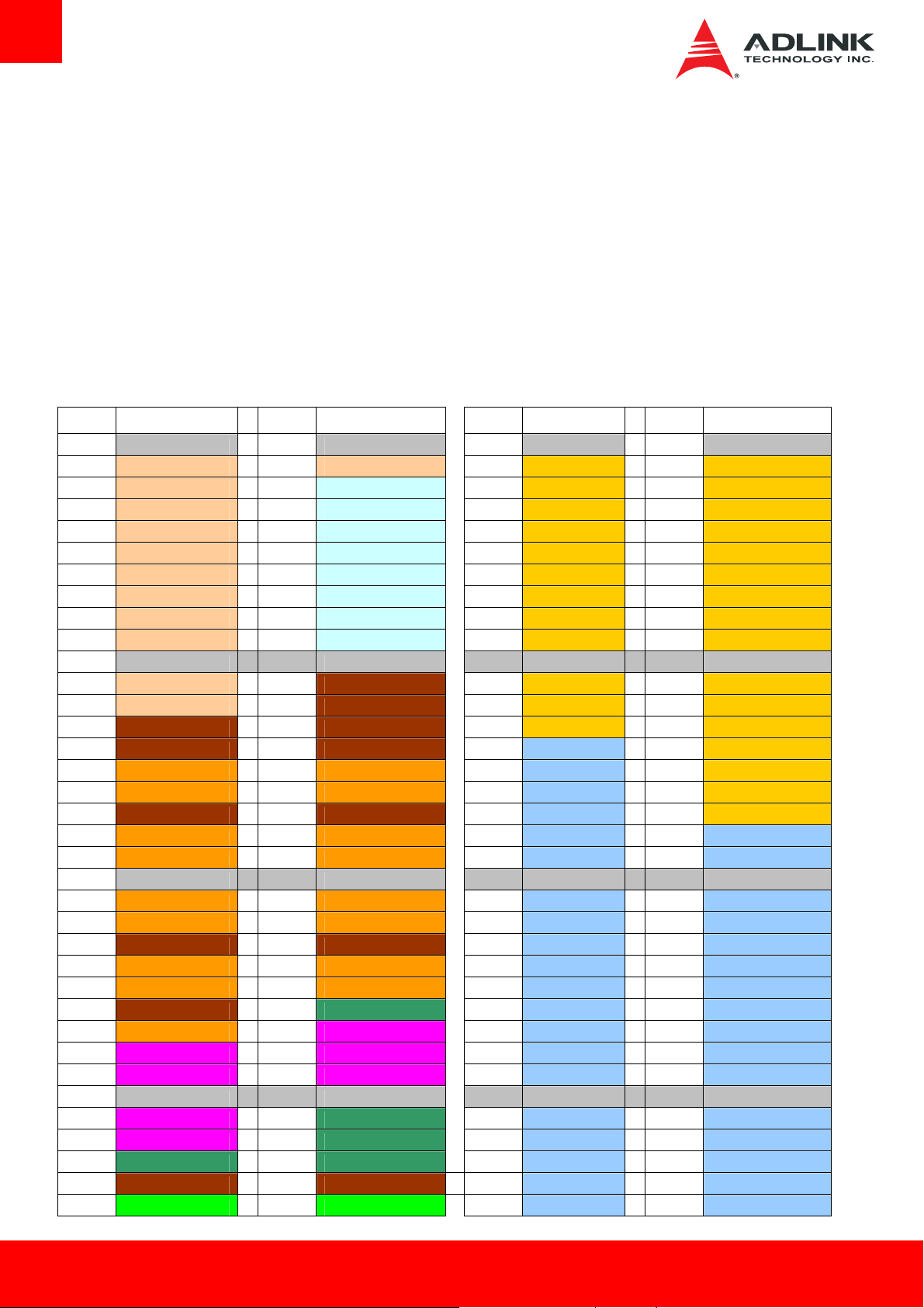
3.1. AB / CD Pin Definitions
All pins in the specification are described, including those not supported on the Express-IB. Those not supported on the Express-IBE2
module are crossed out
Row A Row B Row C Row D
Pin No. Pin Name Pin No. Pin Name Pin No. Pin Name Pin No. Pin Name
A1 GND (FIXED) B1 GND (FIXED) C1 GND FIXED) D1 GND FIXED)
A2 GBE0_MDI3- B2 GBE0_ACT# C2 IDE_D7 D2 IDE_D5
A3 GBE0_MDI3+ B3 LPC_FRAME# C3 IDE_D6 D3 IDE_D10
A4 GBE0_LINK100# B4 LPC_AD0 C4 IDE_D3 D4 IDE_D11
A5 GBE0_LINK1000# B5 LPC_AD1 C5 IDE_D15 D5 IDE_D12
A6 GBE0_MDI2- B6 LPC_AD2 C6 IDE_D8 D6 IDE_D4
A7 GBE0_MDI2+ B7 LPC_AD3 C7 IDE_D9 D7 IDE_D0
A8 GBE0_LINK# B8 LPC_DRQ0# C8 IDE_D2 D8 IDE_REQ
A9 GBE0_MDI1- B9 LPC_DRQ1# C9 IDE_D13 D9 IDE_IOW#
A10 GBE0_MDI1+ B10 LPC_CLK C10 IDE_D1 D10 IDE_ACK#
A11 GND (FIXED) B11 GND (FIXED) C11 GND (FIXED) D11 GND (FIXED)
A12 GBE0_MDI0- B12 PWRBTN# C12 IDE_D14 D12 IDE_IRQ
A13 GBE0_MDI0+ B13 SMB_CK C13 IDE_IORDY D13 IDE_A0
A14 GBE0_CTREF B14 SMB_DAT C14 IDE_IOR# D14 IDE_A1
A15 SUS_S3# B15 SMB_ALERT# C15 PCI_PME# D15 IDE_A2
A16 SATA0_TX+ B16 SATA1_TX+ C16 PCI_GNT2# D16 IDE_CS1#
A17 SATA0_TX- B17 SATA1_TX- C17 PCI_REQ2# D17 IDE_CS3#
A18 SUS_S4# B18 SUS_STAT# C18 PCI_GNT1# D18 IDE_RESET#
A19 SATA0_RX+ B19 SATA1_RX+ C19 PCI_REQ1# D19 PCI_GNT3#
A20 SATA0_RX- B20 SATA1_RX- C20 PCI_GNT0# D20 PCI_REQ3#
A21 GND (FIXED) B21 GND (FIXED) C21 GND (FIXED) D21 GND (FIXED)
A22 SATA2_TX+ B22 SATA3_TX+ C22 PCI_REQ0# D22 PCI_AD1
A23 SATA2_TX- B23 SATA3_TX- C23 PCI_RESET# D23 PCI_AD3
A24 SUS_S5# B24 PWR_OK C24 PCI_AD0 D24 PCI_AD5
A25 SATA2_RX+ B25 SATA3_RX+ C25 PCI_AD2 D25 PCI_AD7
A26 SATA2_RX- B26 SATA3_RX- C26 PCI_AD4 D26 PCI_C/BE0#
A27 BATLOW# B27 WDT C27 PCI_AD6 D27 PCI_AD9
A28 (S)ATA_ACT# B28 AC/HDA_SDIN2 C28 PCI_AD8 D28 PCI_AD11
A29 AC/HDA_SYNC B29 AC/HDA_SDIN1 C29 PCI_AD10 D29 PCI_AD13
A30 AC/HDA_RST# B30 AC/HDA_SDIN0 C30 PCI_AD12 D30 PCI_AD15
A31 GND (FIXED) B31 GND (FIXED) C31 GND (FIXED) D31 GND (FIXED)
A32 AC/HDA_BITCLK B32 SPKR C32 PCI_AD14 D32 PCI_PAR
A33 AC/HDA_SDOUT B33 I2C_CK C33 PCI_C/BE1# D33 PCI_SERR#
A34 BIOS_DIS0# B34 I2C_DAT C34 PCI_PERR# D34 PCI_STOP#
A35 THRMTRIP# B35 THRM# C35 PCI_LOCK# D35 PCI_TRDY#
A36 USB6- B36 USB7- C36 PCI_DEVSEL# D36 PCI_FRAME#
Page 14 Express-IBE2
Page 15
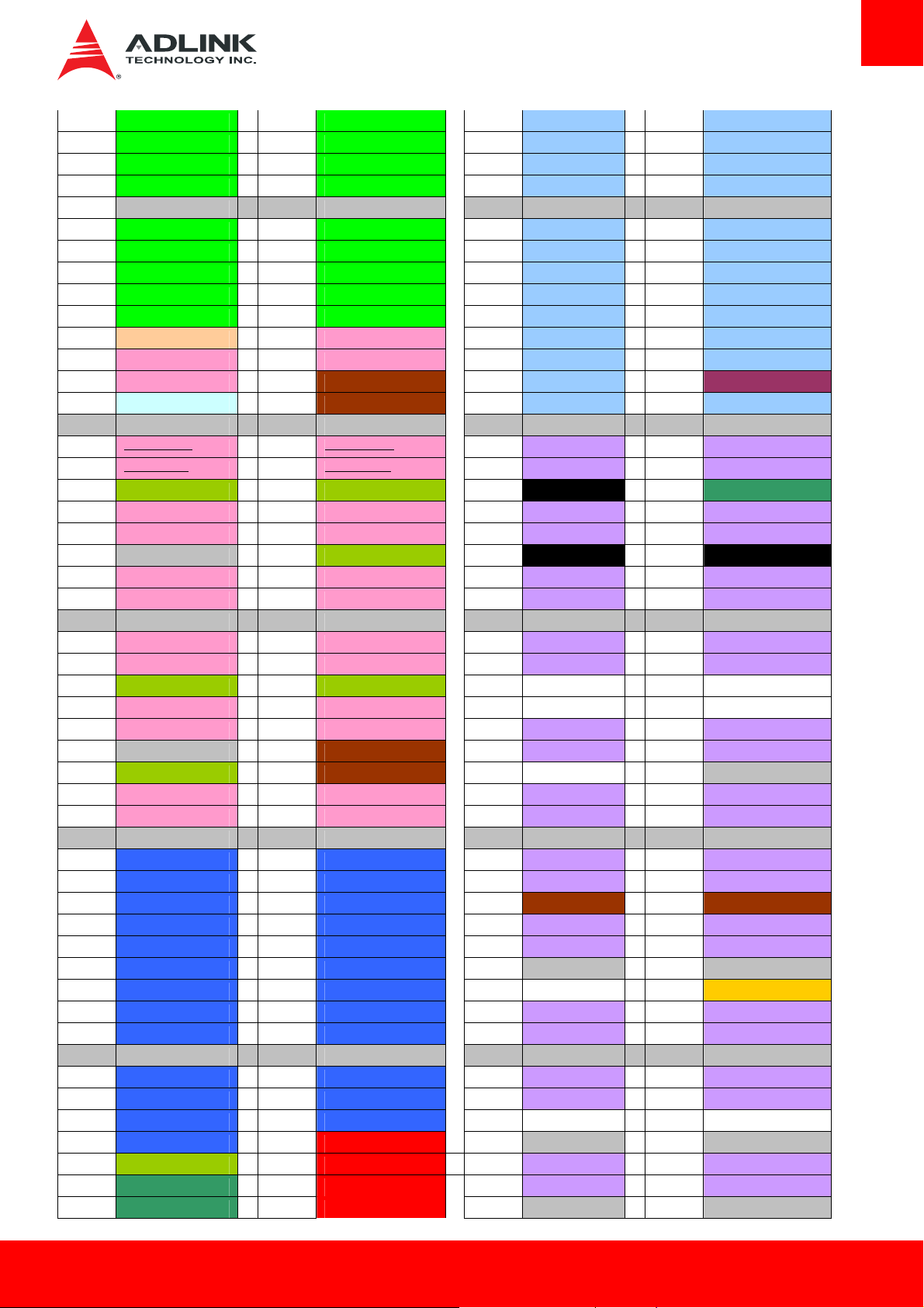
A37 USB6+ B37 USB7+ C37 PCI_IRDY# D37 PCI_AD16
A38 USB_6_7_OC# B38 USB_4_5_OC# C38 PCI_C/BE2# D38 PCI_AD18
A39 USB4- B39 USB5- C39 PCI_AD17 D39 PCI_AD20
A40 USB4+ B40 USB5+ C40 PCI_AD19 D40 PCI_AD22
A41 GND (FIXED) B41 GND (FIXED) C41 GND (FIXED) D41 GND (FIXED)
A42 USB2- B42 USB3- C42 PCI_AD21 D42 PCI_AD24
A43 USB2+ B43 USB3+ C43 PCI_AD23 D43 PCI_AD26
A44 USB_2_3_OC# B44 USB_0_1_OC# C44 PCI_C/BE3# D44 PCI_AD28
A45 USB0- B45 USB1- C45 PCI_AD25 D45 PCI_AD30
A46 USB0+ B46 USB1+ C46 PCI_AD27 D46 PCI_IRQC#
A47 VCC_RTC B47 EXCD1_PERST# C47 PCI_AD29 D47 PCI_IRQD#
A48 EXCD0_PERST# B48 EXCD1_CPPE# C48 PCI_AD31 D48 PCI_CLKRUN#
A49 EXCD0_CPPE# B49 SYS_RESET# C49 PCI_IRQA# D49 PCI_M66EN (GND)
A50 LPC_SERIRQ B50 CB_RESET# C50 PCI_IRQB# D50 PCI_CLK
A51 GND (FIXED) B51 GND (FIXED) C51 GND (FIXED) D51 GND (FIXED)
A52 PCIE_TX5+ B52 PCIE_RX5+ C52 PEG_RX0+ D52 PEG_TX0+
A53 PCIE_TX5- B53 PCIE_RX5- C53 PEG_RX0- D53 PEG_TX0A54 GPI0 B54 GPO1 C54 TYPE0# D54 PEG_LANE_RV#
A55 PCIE_TX4+ B55 PCIE_RX4+ C55 PEG_RX1+ D55 PEG_TX1+
A56 PCIE_TX4- B56 PCIE_RX4- C56 PEG_RX1- D56 PEG_TX1A57 GND B57 GPO2 C57 TYPE1# D57 TYPE2#
A58 PCIE_TX3+ B58 PCIE_RX3+ C58 PEG_RX2+ D58 PEG_TX2+
A59 PCIE_TX3- B59 PCIE_RX3- C59 PEG_RX2- D59 PEG_TX2A60 GND (FIXED) B60 GND (FIXED) C60 GND (FIXED) D60 GND (FIXED)
A61 PCIE_TX2+ B61 PCIE_RX2+ C61 PEG_RX3+ D61 PEG_TX3+
A62 PCIE_TX2- B62 PCIE_RX2- C62 PEG_RX3- D62 PEG_TX3A63 GPI1 B63 GPO3 C63 RSVD D63 RSVD
A64 PCIE_TX1+ B64 PCIE_RX1+ C64 RSVD D64 RSVD
A65 PCIE_TX1- B65 PCIE_RX1- C65 PEG_RX4+ D65 PEG_TX4+
A66 GND B66 WAKE0# C66 PEG_RX4- D66 PEG_TX4-
A67 GPI2 B67 WAKE1# C67 RSVD D67 GND
A68 PCIE_TX0+ B68 PCIE_RX0+ C68 PEG_RX5+ D68 PEG_TX5+
A69 PCIE_TX0- B69 PCIE_RX0- C69 PEG_RX5- D69 PEG_TX5A70 GND (FIXED) B70 GND (FIXED) C70 GND (FIXED) D70 GND (FIXED)
A71 LVDS_A0+ B71 LVDS_B0+ C71 PEG_RX6+ D71 PEG_TX6+
A72 LVDS_A0- B72 LVDS_B0- C72 PEG_RX6- D72 PEG_TX6A73 LVDS_A1+ B73 LVDS_B1+ C73 SDVO_DATA D73 SDVO_CLK
A74 LVDS_A1- B74 LVDS_B1- C74 PEG_RX7+ D74 PEG_TX7+
A75 LVDS_A2+ B75 LVDS_B2+ C75 PEG_RX7- D75 PEG_TX7A76 LVDS_A2- B76 LVDS_B2- C76 GND D76 GND
A77 LVDS_VDD_EN B77 LVDS_B3+ C77 RSVD D77 IDE_CBLID#
A78 LVDS_A3+ B78 LVDS_B3- C78 PEG_RX8+ D78 PEG_TX8+
A79 LVDS_A3- B79 LVDS_BKLT_EN C79 PEG_RX8- D79 PEG_TX8A80 GND (FIXED) B80 GND (FIXED) C80 GND (FIXED) D80 GND (FIXED)
A81 LVDS_A_CK+ B81 LVDS_B_CK+ C81 PEG_RX9+ D81 PEG_TX9+
A82 LVDS_A_CK- B82 LVDS_B_CK- C82 PEG_RX9- D82 PEG_TX9A83 LVDS_I2C_CK B83 LVDS_BKLT_CTRL C83 RSVD D83 RSVD
A84 LVDS_I2C_DAT B84 VCC_5V_SBY C84 GND D84 GND
A85 GPI3 B85 VCC_5V_SBY C85 PEG_RX10+ D85 PEG_TX10+
A86 KBD_RST# B86 VCC_5V_SBY C86 PEG_RX10- D86 PEG_TX10A87 KBD_A20GATE B87 VCC_5V_SBY C87 GND D87 GND
Express-IBE2 Page 15
Page 16
A88 PCIE0_CK_REF+ B88 BIOS_DIS1# C88 PEG_RX11+ D88 PEG_TX11+
A89 PCIE0_CK_REF- B89 VGA_RED C89 PEG_RX11- D89 PEG_TX11A90 GND (FIXED) B90 GND (FIXED) C90 GND (FIXED) D90 GND (FIXED)
A91 SPI_POWER B91 VGA_GRN C91 PEG_RX12+ D91 PEG_TX12+
A92 SPI_MISO B92 VGA_BLU C92 PEG_RX12- D92 PEG_TX12-
A93 GPO0 B93 VGA_HSYNC C93 GND D93 GND
A94 SPI_CLK B94 VGA_VSYNC C94 PEG_RX13+ D94 PEG_TX13+
A95 SPI_MOSI B95 VGA_I2C_CK C95 PEG_RX13- D95 PEG_TX13-
A96 GND B96 VGA_I2C_DAT C96 GND D96 GND
A97 TYPE10# B97 SPI_CS# C97 RSVD D97 PEG_ENABLE#
A98 RSVD B98 RSVD C98 PEG_RX14+ D98 PEG_TX14+
A99 RSVD B99 RSVD C99 PEG_RX14- D99 PEG_TX14A100 GND (FIXED) B100 GND (FIXED) C100 GND (FIXED) D100 GND (FIXED)
A101 RSVD B101 RSVD C101 PEG_RX15+ D101 PEG_TX15+
A102 RSVD B102 RSVD C102 PEG_RX15- D102 PEG_TX15A103 RSVD B103 RSVD C103 GND D103 GND
A104 VCC_12V B104 VCC_12V C104 VCC_12V D104 VCC_12V
A105 VCC_12V B105 VCC_12V C105 VCC_12V D105 VCC_12V
A106 VCC_12V B106 VCC_12V C106 VCC_12V D106 VCC_12V
A107 VCC_12V B107 VCC_12V C107 VCC_12V D107 VCC_12V
A108 VCC_12V B108 VCC_12V C108 VCC_12V D108 VCC_12V
A109 VCC_12V B109 VCC_12V C109 VCC_12V D109 VCC_12V
A110 GND (FIXED) B110 GND (FIXED) C110 GND (FIXED) D110 GND (FIXED)
Page 16 Express-IBE2
Page 17

3.2. Signal Description Terminology
These terms are used in the COM Express AB/CD Signal Descriptions which follow.
I Input to the Module
O Output from the Module
I/O Bi-directional input/output signal
OD Open drain output
I 3.3V Input 3.3V tolerant
I 5V Input 5V tolerant
O 3.3V Output 3.3V signal level
O 5V Output 5V signal level
I/O 3.3V Bi-directional signal 3.3V tolerant
I/O 5V Bi-directional signal 5V tolerant
I/O 3.3Vsb Input 3.3V tolerant active in standby state
P Power Input/Output
REF Reference voltage output that may be sourced from a module power plane.
PDS Pull-down strap. This is an output pin on the module that is either tied to GND, or not connected.
The signal is used to indicate the PICMG module type to the Carrier Board.
PU ADLINK implemented pull-up resistor on module
PD ADLINK implemented pull-down resistor on module
Express-IBE2 Page 17
Page 18
3.3. AB Signal Descriptions
3.3.1. Audio Signals
Signal Pin Description I/O PU/PD Comment
AC_RST# /
HDA_RST#
AC_SYNC /
HDA_SYNC
AC_BITCLK /
HDA_BITCLK
AC _SDOUT /
HDA_SDOUT
AC _SDIN[2:0]
HDA_SDIN[2:0]
A30 Reset output to CODEC, active low. O 3.3VSB
A29 Sample-synchronization signal to the CODEC(s). O 3.3V
A32 Serial data clock generated by the external
CODEC(s).
A33 Serial TDM data output to the CODEC. O 3.3V
B28
B30
Serial TDM data inputs from up to 3 CODECs. I/O 3.3VSB
I/O 3.3V
3.3.2. Analog VGA
Signal Pin Description I/O PU/PD Comment
VGA_RED B89 Red for monitor.
Analog DAC output, designed to drive a
37.5-Ohm equivalent load.
VGA_GRN B91 Green for monitor
Analog DAC output, designed to drive a
37.5-Ohm equivalent load.
O Analog If VGA is used, signal should be
pulled to GND by 150Ω on the
carrier
O Analog If VGA is used, signal should be
pulled to GND by 150Ω on the
carrier
VGA_BLU B92 Blue for monitor.
Analog DAC output, designed to drive a
37.5-Ohm equivalent load.
VGA_HSYNC B93 Horizontal sync output to VGA monitor O 3.3V
VGA_VSYNC B94 Vertical sync output to VGA monitor O 3.3V
VGA_I2C_CK B95 DDC clock line (I²C port dedicated to identify
VGA monitor capabilities)
VGA_I2C_DAT B96 DDC data line. I/O OD 3.3V PU 2k2 3.3V
O Analog If VGA is used, signal should be
I/O OD 3.3V PU 2k2 3.3V
pulled to GND by 150Ω on the
carrier
Page 18 Express-IBE2
Page 19
3.3.3. LVDS
Signal Pin Description I/O PU/PD Comment
LVDS_A0+
LVDS_A0-
LVDS_A1+
LVDS_A1-
LVDS_A2+
LVDS_A2-
LVDS_A3+
LVDS_A3-
LVDS_A_CK+
LVDS_A_CK-
LVDS_B0+
LVDS_B0-
LVDS_B1+
LVDS_B1-
LVDS_B2+
LVDS_B2-
LVDS_B3+
LVDS_B3-
LVDS_B_CK+
LVDS_B_CK-
LVDS_VDD_EN A77 LVDS panel power enable O 3.3V
LVDS_BKLT_EN B79 LVDS panel backlight enable O 3.3V
LVDS_BKLT_CTRL B83 LVDS panel backlight brightness control O 3.3V
LVDS_I2C_CK A83 DDC lines used for flat panel detection and control. O 3.3V PU 2k2 3.3V
A71
A72
A73
A74
A75
A76
A78
A79
A81
A82
B71
B72
B73
B74
B75
B76
B77
B78
B81
B82
LVDS Channel A differential pairs O LVDS
LVDS Channel A differential clock O LVDS
LVDS Channel B differential pairs O LVDS
LVDS Channel B differential clock O LVDS
LVDS_I2C_DAT A84 DDC lines used for flat panel detection and control. I/O 3.3V PU 2k2 3.3V
3.3.4. Gigabit Ethernet
Gigabit Ethernet Pin Description I/O PU/PD Comment
GBE0_MDI0+
GBE0_MDI0-
GBE0_MDI1+
GBE0_MDI1-
GBE0_MDI2+
GBE0_MDI2-
GBE0_MDI3+
GBE0_MDI3-
GBE0_ACT# B2 Gigabit Ethernet Controller 0 activity indicator, active low. OD 3.3VSB PU 1k
GBE0_LINK# A8 Gigabit Ethernet Controller 0 link indicator, active low. OD 3.3VSB
GBE0_LINK100# A4 Gigabit Ethernet Controller 0 100Mbit/sec link indicator, active low. OD 3.3VSB
GBE0_LINK1000# A5 Gigabit Ethernet Controller 0 1000Mbit/sec link indicator, active low. OD 3.3VSB
GBE0_CTREF A14 Reference voltage for Carrier Board Ethernet channel 1 and 2
A13
A12
A10
A9
A7
A6
A3
A2
Gigabit Ethernet Controller 0: Media Dependent Interface Differential
Pairs 0, 1, 2, 3. The MDI can operate in 1000, 100, and 10Mbit/sec
modes. Some pairs are unused in some modes, as described here:
1000BASE-T 100BASE-TX 10BASE-T
MDI[0]+/- B1_DA+/- TX+/- TX+/-
MDI[1]+/- B1_DB+/- RX+/- RX+/-
MDI[2]+/- B1_DC+/MDI[3]+/- B1_DD+/-
magnetics center tap. The reference voltage is determined by the
requirements of the Module PHY and may be as low as 0V and as high
as 3.3V. The reference voltage output shall be current limited on the
Module. Where the reference is shorted to ground, the current shall be
250 mA or less.
I/O Analog Twisted pair
signals for
external
transformer.
3.3V
GND min
3.3V max
Express-IBE2 Page 19
Page 20
3.3.5. Serial ATA
Signal Pin Description I/O PU/PD Comment
SATA0_TX+
SATA0_TX-
SATA0_RX+
SATA0_RX-
SATA1_TX+
SATA1_TX-
SATA1_RX+
SATA1_RX-
SATA2_TX+
SATA2_TX-
SATA2_RX+
SATA2_RX-
SATA3_TX+
SATA3_TX-
SATA3_RX+
SATA3_RX-
(S)ATA_ACT# A28 ATA (parallel and serial) or SAS activity
A16
A17
A19
A20
B16
B17
B19
B20
A22
A23
A25
A26
B22
B23
B25
B26
Serial ATA channel 0, Transmit Output
differential pair.
Serial ATA channel 0, Receive Input
differential pair.
Serial ATA channel 1, Transmit Output
differential pair.
Serial ATA channel 1, Receive Input
differential pair.
Serial ATA channel 2, Transmit Output
differential pair.
Serial ATA channel 2, Receive Input
differential pair.
Serial ATA channel 3, Transmit Output
differential pair.
Serial ATA channel 3, Receive Input
differential pair.
indicator, active low.
O SATA AC coupled on Module
I SATA AC coupled on Module
O SATA AC coupled on Module
I SATA AC coupled on Module
O SATA AC coupled on Module
I SATA AC coupled on Module
O SATA AC coupled on Module
I SATA AC coupled on Module
O 3.3V
Page 20 Express-IBE2
Page 21
3.3.6. PCI Express
Signal Pin Description I/O PU/PD Comment
PCIE_TX0+
PCIE_TX0-
PCIE_RX0+
PCIE_RX0-
PCIE_TX1+
PCIE_TX1-
PCIE_RX1+
PCIE_RX1-
PCIE_TX2+
PCIE_TX2-
PCIE_RX2+
PCIE_RX2-
PCIE_TX3+
PCIE_TX3-
PCIE_RX3+
PCIE_RX3-
PCIE_TX4+
PCIE_TX4-
PCIE_RX4+
PCIE_RX4-
A68
A69
B68
B69
A64
A65
B64
B65
A61
A62
B61
B62
A58
A59
B58
B59
A55
A56
B55
B56
PCI Express channel 0, Transmit Output differential pair. O PCIE AC coupled on Module
PCI Express channel 0, Receive Input differential pair. I PCIE AC coupled off Module
PCI Express channel 1, Transmit Output differential pair. O PCIE AC coupled on Module
PCI Express channel 1, Receive Input differential pair. I PCIE AC coupled off Module
PCI Express channel 2, Transmit Output differential pair. O PCIE AC coupled on Module
PCI Express channel 2, Receive Input differential pair. I PCIE AC coupled off Module
PCI Express channel 3, Transmit Output differential pair. O PCIE AC coupled on Module
PCI Express channel 3, Receive Input differential pair. I PCIE AC coupled off Module
PCI Express channel 4, Transmit Output differential pair. O PCIE AC coupled on Module
PCI Express channel 4, Receive Input differential pair. I PCIE AC coupled off Module
PCIE_TX5+
PCIE_TX5-
PCIE_RX5+
PCIE_RX5-
PCIE_CLK_REF+
PCIE_CLK_REF-
A52
A53
B52
B53
A88
A89
PCI Express channel 5, Transmit Output differential pair. O PCIE not supported on this module
PCI Express channel 5, Receive Input differential pair. I PCIE not supported on this module
PCI Express Reference Clock output for all PCI Express
and PCI Express Graphics Lanes.
O PCIE
3.3.7. Express Card
Signal Pin Description I/O PU/PD Comment
EXCD0_CPPE#
EXCD1_CPPE#
EXCD0_PERST#
EXCD1_PERST#
A49
B48
A48
B47
PCI ExpressCard: PCI Express capable card request I 3.3V PU 10k 3.3V
PCI ExpressCard: reset O 3.3V
Express-IBE2 Page 21
Page 22

3.3.8. LPC bus
Signal Pin Description I/O PU/PD Comment
LPC_AD[0:3] B4-B7 LPC multiplexed address, command and data bus I/O 3.3V
LPC_FRAME# B3 LPC frame indicates the start of an LPC cycle O 3.3V
LPC_DRQ0#
LPC_DRQ1#
LPC_SERIRQ A50 LPC serial interrupt I/O OD 3.3V PU 8k2 3.3V
LPC_CLK B10 LPC clock output - 33MHz nominal O 3.3V
B8
B9
LPC serial DMA request I 3.3V
3.3.9. USB
Signal Pin Description I/O PU/PD Comment
USB0+
USB0-
USB1+
USB1-
USB2+
USB2-
USB3+
USB3-
USB4+
USB4-
USB5+
USB5-
A46
USB differential data pairs for Port 0 I/O 3.3VSB USB 1.1/ 2.0 compliant
A45
B46
USB differential data pairs for Port 1 I/O 3.3VSB USB 1.1/ 2.0 compliant
B45
A43
USB differential data pairs for Port 1 I/O 3.3VSB USB 1.1/ 2.0 compliant
A42
B43
USB differential data pairs for Port 2 I/O 3.3VSB USB 1.1/ 2.0 compliant
B42
A40
USB differential data pairs for Port 3 I/O 3.3VSB USB 1.1/ 2.0 compliant
A39
B40
USB differential data pairs for Port 4 I/O 3.3VSB USB 1.1/ 2.0 compliant
B39
USB6+
USB6-
USB7+
USB7-
USB_0_1_OC# B44 USB over-current sense, USB ports 0 and 1. A pull-up
USB_2_3_OC# A44 USB over-current sense, USB ports 2 and 3. A pull-up
USB_4_5_OC# B38 USB over-current sense, USB ports 4 and 5. A pull-up
USB_6_7_OC# A38 USB over-current sense, USB ports 6 and 7. A pull-up
A37
USB differential data pairs for Port 5 I/O 3.3VSB USB 1.1/ 2.0 compliant
A36
B37
USB differential data pairs for Port 6 I/O 3.3VSB USB 1.1/ 2.0 compliant
B37
for this line shall be present on the module. An open
drain driver from a USB current monitor on the carrier
board may drive this line low.
for this line shall be present on the module. An open
drain driver from a USB current monitor on the carrier
board may drive this line low.
for this line shall be present on the module. An open
drain driver from a USB current monitor on the carrier
board may drive this line low.
for this line shall be present on the module. An open
drain driver from a USB current monitor on the carrier
board may drive this line low.
I 3.3VSB PU 10k 3.3VSB Do not pull high on carrier
I 3.3VSB PU 10k 3.3VSB Do not pull high on carrier
I 3.3VSB PU 10k 3.3VSB Do not pull high on carrier
I 3.3VSB PU 10k 3.3VSB Do not pull high on carrier
Page 22 Express-IBE2
Page 23
3.3.10. SPI (BIOS only)
Signal Pin Description I/O PU/PD Comment
SPI_CS# B97 Chip select for Carrier Board SPI BIOS Flash. O 3.3VSB
SPI_MISO A92 Data in to module from carrier board SPI BIOS flash. I 3.3VSB
SPI_MOSI A95 Data out from module to carrier board SPI BIOS flash. O 3.3VSB
SPI_CLK A94 Clock from module to carrier board SPI BIOS flash. O 3.3VSB
SPI_POWER A91 Power supply for Carrier Board SPI – sourced from Module
– nominally 3.3V. The Module shall provide a minimum of
100mA on SPI_POWER. Carriers shall use less than
100mA of SPI_POWER. SPI_POWER shall only be used
to power SPI devices on the Carrier
BIOS_DIS0# A34 Selection strap to determine the BIOS boot device. I PU 10K 3.3V Carrier shall pull to GND
BIOS_DIS1# B88 Selection strap to determine the BIOS boot device. I PU 10K 3.3V Carrier shall pull to GND
O P 3.3VSB
or leave unconnected
or leave unconnected
3.3.11. Miscellaneous
Signal Pin Description I/O PU/PD Comment
SPKR B32 Output for audio enunciator, the “speaker” in PC-AT
systems.
WDT B27 Output indicating that a watchdog time-out event has
occurred.
KBD_RST# A86 Input to module from (optional) external keyboard
controller which can force a reset. Pulled high on the
module. This is a legacy artifact of the PC-AT.
KBD_A20GATE A87 Input to module from (optional) external keyboard
controller which can be used to control the CPU A20 gate
line. The A20GATE restricts the memory access to the
bottom megabyte and is a legacy artifact of the PC-AT.
Pulled low on the module.
THRM# B35 Input from off-module temp sensor indicating an over-temp
situation.
O 3.3V
O 3.3V
I 3.3V PU 10K 3.3V
I 3.3V PU 10K 3.3V
I 3.3V
THERMTRIP# A35 Active low output indicating the CPU has entered thermal
shutdown.
TPM_PP11 C83 Trusted Platform Module (TPM) Physical Presence pin.
Active high. TPM chip has an internal pull down. This
signal is used to indicate Physical Presence to the TPM.
O 3.3V
I 3.3V PD 3.3V If TPM not installed on
module, remove PD
3.3V
Express-IBE2 Page 23
Page 24
3.3.12. SMBus
Signal Pin Description I/O PU/PD Comment
SMB_CK B13 System Management Bus bidirectional clock line. Power
sourced through 5V standby rail and main power rails.
SMB_DAT# B14 System Management Bus bidirectional data line. Power
sourced through 5V standby rail and main power rails.
SMB_ALERT# B15 System Management Bus Alert – active low input can
be used to generate an SMI# (System Management
Interrupt) or to wake the system. Power sourced
through 5V standby rail and main power rails.
I/O OD 3.3VSB PU 2k2 3.3VSB
I/O OD 3.3VSB PU 2k2 3.3VSB
I 3.3VSB PU 10k 3.3VSB
3.3.13. I2C Bus
Signal Pin Description I/O PU/PD Comment
I2C_CK B33 General purpose I²C port clock output/input I/O OD 3.3VSB PU 2k2 3.3VSB
I2C_DAT B34 General purpose I²C port data I/O line I/O OD 3.3VSB PU 2k2 3.3VSB
3.3.14. General Purpose I/O (GPIO)
Signal Pin Description I/O PU/PD Comment
GPO[0] A93 General purpose output pins. O 3.3V
GPO[1] B54 General purpose output pins. O 3.3V
GPO[2] B57 General purpose output pins. O 3.3V
GPO[3] B63 General purpose output pins. O 3.3V
GPI[0] A54 General purpose input pins. Pulled high internally on the module. I 3.3V PU 10K 3.3V
GPI[1] A63 General purpose input pins. Pulled high internally on the module. I 3.3V PU 10K 3.3V
GPI[2] A67 General purpose input pins. Pulled high internally on the module. I 3.3V PU 10K 3.3V
GPI[3] A85 General purpose input pins. Pulled high internally on the module. I 3.3V PU 10K 3.3V
Page 24 Express-IBE2
Page 25
3.3.15. Power And System Management
Signal Pin Description I/O PU/PD Comment
PWRBTN# B12 Power button to bring system out of S5 (soft off), active on falling edge. I 3.3VSB PU 10k 3.3VSB
SYS_RESET# B49 Reset button input. Active low request for module to reset and reboot. May
be falling edge sensitive. For situations when SYS_RESET# is unable to
reestablish control of the system, PWR_OK or a power cycle may be used.
CB_RESET# B50 Reset output from module to Carrier Board. Active low. Issued by module
chipset and may result from a low SYS_RESET# input, a low PWR_OK
input, a VCC_12V power input that falls below the minimum specification, a
watchdog timeout, or may be initiated by the module software.
PWR_OK B24 Power OK from main power supply. A high value indicates that the power is
good. This signal can be used to hold off Module startup, to allow carrier
based FPGAs or other configurable devices time to be programmed.
SUS_STAT# B18 Indicates imminent suspend operation; used to notify LPC devices. O 3.3VSB
SUS_S3# A15 Indicates system is in Suspend to RAM state. Active-low output. An inverted
copy of SUS_S3# on the carrier board (also known as “PS_ON”) may be
used to enable the non-standby power on a typical ATX power supply.
SUS_S4# A18 Indicates system is in Suspend to Disk state. Active low output. O 3.3VSB
SUS_S5# A24 Indicates system is in Soft Off state. O 3.3VSB
WAKE0# B66 PCI Express wake up signal. I 3.3VSB PU 10k 3.3VSB
WAKE1# B67 General purpose wake up signal. May be used to implement wake-up on
PS/2 keyboard or mouse activity.
BATLOW# A27 Battery low input. This signal may be driven low by external circuitry to signal
that the system battery is low, or may be used to signal some other e xternal
power-management event.
I 3.3VSB PU 10k 3.3VSB
O 3.3VSB
I 3.3V PU 10k 3.3V
O 3.3VSB
I 3.3VSB PU 10k 3.3VSB
I 3.3VSB PU 10k 3.3VSB
PU 10k 3.3VSB
Express-IBE2 Page 25
Page 26

3.3.16. Power and Ground
Signal Pin Description I/O PU/PD Comment
VCC_12V A104-A109
B104-B109
VCC_5V_SBY B84-B87 Standby power input: +5.0V nominal. See section 7 “Electrical
VCC_RTC A47 Real-time clock circuit-power input. Nominally +3.0V. P
GND A1, A11, A21, A31,
A41, A51, A57, A66,
A80, A90, A96,
A100, A110, B1,
B11, B21 ,B31, B41,
B51, B60, B70, B80,
B90, B100, B110
Primary power input: +12V nominal (5 ~ 19V). See section 7
“Electrical Specifications“ for allowable input range. All available
VCC_12V pins on the connector(s) shall be used.
Specifications“ for allowable input range. If VCC5_SBY is used,
all available VCC_5V_SBY pins on the connector(s) shall be used.
Only used for standby and suspend functions. May be left
unconnected if these functions are not used in the system design.
Ground - DC power and signal and AC signal return path. P
P 8.5~20 V
P 5Vsb ±5%
Page 26 Express-IBE2
Page 27

3.4. CD Signal Descriptions
3.4.1. PATA IDE
Signal Pin Description I/O PU/PD Comment
IDE_D0
IDE_D1
IDE_D2
IDE_D3
IDE_D4
IDE_D5
IDE_D6
IDE_D7
IDE_D8
IDE_D9
IDE_D10
IDE_D11
IDE_D12
IDE_D13
IDE_D14
IDE_D15
IDE_A0 D13 Address lines to IDE device. O 3.3V
IDE_A1 D14 Address lines to IDE device. O 3.3V
IDE_A2 D15 Address lines to IDE device. O 3.3V
IDE_IOW# D9 I/O write line to IDE device. Data latched on trailing (rising) edge. O 3.3V
IDE_IOR# C14 I/O read line to IDE device. O 3.3V
IDE_REQ D8 IDE Device DMA Request. It is asserted by the IDE device to request a data transfer. I 3.3V
IDE_ACK# D10 IDE Device DMA Acknowledge. O 3.3V
D7
Bidirectional data to / from IDE device. I/O
C10
C8
C4
D6
D2
C3
C2
C6
C7
D3
D4
D5
C9
C12
C5
3.3V
IDE_CS1# D16 IDE Device Chip Select for 1F0h to 1FFh range. O 3.3V
IDE_CS3# D17 IDE Device Chip Select for 3F0h to 3FFh range. O 3.3V
IDE_IORDY C13 IDE device I/O ready input. Pulled low by the IDE device to extend the cycle. I 3.3V PU 4k7 3.3V
IDE_RESET# D18 Reset output to IDE device, active low. O 3.3V
IDE_IRQ D12 Interrupt request from IDE device. I 3.3V PD 10k shall
IDE_CBLID# D77 Input from off-module hardware indicating the type of IDE cable being used. High
indicates a 40-pin cable used for legacy IDE modes. Low indicates that an 80-pin
cable with interleaved grounds is used. Such a cable is required for Ultra-DMA 66,
100 and 133 modes.
I 3.3V
Express-IBE2 Page 27
Page 28

3.4.2. PCI
Signal Pin Description I/O PU/PD Comment
PCI_AD0
PCI_AD1
PCI_AD2
PCI_AD3
PCI_AD4
PCI_AD5
PCI_AD6
PCI_AD7
PCI_AD8
PCI_AD9
PCI_AD10
PCI_AD11
PCI_AD12
PCI_AD13
PCI_AD14
PCI_AD15
PCI_AD16
PCI_AD17
PCI_AD18
PCI_AD19
PCI_AD20
PCI_AD21
PCI_AD22
PCI_AD23
PCI_AD24
PCI_AD25
PCI_AD26
PCI_AD27
PCI_AD28
PCI_AD29
PCI_AD30
PCI_AD31
C24
PCI bus multiplexed address and data lines I/O 3.3V
D22
C25
D23
C26
D24
C27
D25
C28
D27
C29
D28
C30
D29
C32
D30
D37
C39
D38
C40
D39
C42
D40
C43
D42
C45
D43
C46
D44
C47
D45
C48
PCI_C/BE0#
PCI_C/BE1#
PCI_C/BE2#
PCI_C/BE3#
PCI_DEVSEL# C36 PCI bus Device Select, active low. I/O 3.3V PU 8k2 3.3V
PCI_FRAME# D36 PCI bus Frame control line, active low. I/O 3.3V PU 8k2 3.3V
PCI_IRDY# C37 PCI bus Initiator Ready control line, active low. I/O 3.3V PU 8k2 3.3V
PCI_TRDY# D35 PCI bus Target Ready control line, active low. I/O 3.3V PU 8k2 3.3V
PCI_STOP# D34 PCI bus STOP control line, active low, driven by cycle initiator. I/O 3.3V PU 8k2 3.3V
PCI_PAR D32 PCI bus parity I/O 3.3V
PCI_PERR# C34 Parity Error: an external PCI device drives PERR# when it
PCI_REQ0#
PCI_REQ1#
PCI_REQ2#
PCI_REQ3#
PCI_GNT0#
PCI_GNT1#
PCI_GNT2#
PCI_GNT3#
PCI_RESET# C23 PCI Reset output, active low. O 3.3V
D26
PCI bus byte enable lines, active low. I/O 3.3V
C33
C38
C44
I/O 3.3V PU 8k2 3.3V
receives data containing a parity error.
C22
PCI bus master request input lines, active low. I 3.3V PU 8k2 3.3V
C19
C17
D20
C20
PCI bus master grant output lines, active low. O 3.3V
C18
C16
D19
Page 28 Express-IBE2
Page 29

Signal Pin Description I/O PU/PD Comment
PCI_LOCK# C35 PCI Lock control line, active low. I/O 3.3V PU 8k2 3.3V
PCI_SERR# D33 System Error: SERR# may be pulsed active by any PCI device
that detects a system error condition.
PCI_PME# C15 PCI Power Management Event: PCI peripherals drive PME# to
wake system from low-power states S1–S5.
PCI_CLKRUN# D48 Bidirectional pin used to support PCI clock run protocol for
mobile systems.
PCI_IRQA# PCI_IRQB#
PCI_IRQC# PCI_IRQD#
PCI_CLK D50 PCI 33MHz clock output O 3.3V
PCI_M66EN D49 Module input signal indicates whether an off-Module PCI device
C49
PCI interrupt request lines I 3.3V PU 8k2 3.3V
C50
D46
D47
is capable of 66MHz operation. Pulled to GND by Carrier Board
device or by Slot Card if the devices are NOT capable of 66
MHz operation.
If the Module is not capable of supporting 66 MHz PCI
operation, this input may be a no-connect on the Module.
If the Module is capable of supporting 66 MHz PCI operation,
and if this input is held low by the Carrier Board, the Module PCI
interface shall operate at 33 MHz.
I/O 3.3V PU 8k2 3.3V
I 3.3VSB
I/O 3.3V PU 10k 3.3V
Express-IBE2 Page 29
Page 30

3.4.3. PCI Express Graphics x16 (PEG) or SDVO
PEG x16 mode
Signal Pin Description I/O PU/PD Comment
PEG_RX0+
PEG_RX0PEG_RX1+
PEG_RX1PEG_RX2+
PEG_RX2PEG_RX3+
PEG_RX3PEG_RX4+
PEG_RX4PEG_RX5+
PEG_RX5PEG_RX6+
PEG_RX6PEG_RX7+
PEG_RX7PEG_RX8+
PEG_RX8PEG_RX9+
PEG_RX9PEG_RX10+
PEG_RX10PEG_RX11+
PEG_RX11PEG_RX12+
PEG_RX12PEG_RX13+
PEG_RX13PEG_RX14+
PEG_RX14PEG_RX15+
PEG_RX15
C52
PCI Express Graphics transmit differential pairs. I PCIE
C53
C55
C56
C58
C59
C61
C62
C65
C66
C68
C69
C71
C72
C74
C75
C78
C79
C81
C82
C85
C86
C88
C89
C91
C92
C94
C95
C98
C99
C101
C102
PEG_TX0+
PEG_TX0PEG_TX1+
PEG_TX1PEG_TX2+
PEG_TX2PEG_TX3+
PEG_TX3PEG_TX4+
PEG_TX4PEG_TX5+
PEG_TX5PEG_TX6+
PEG_TX6PEG_TX7+
PEG_TX7PEG_TX8+
PEG_TX8PEG_TX9+
PEG_TX9PEG_TX10+
PEG_TX10PEG_TX11+
PEG_TX11PEG_TX12+
PEG_TX12PEG_TX13+
PEG_TX13PEG_TX14+
D52
PCI Express Graphics receive differential pairs. O PCIE
D53
D55
D56
D58
D57
D61
D62
D65
D66
D68
D69
D71
D72
D74
D75
D78
D79
D81
D82
D85
D86
D88
D89
D91
D92
D94
D95
D98
Page 30 Express-IBE2
Page 31

Signal Pin Description I/O PU/PD Comment
PEG_TX14PEG_TX15+
PEG_TX15-
D99
D101
D102
PEG_LANE_RV# D54 PCI Express Graphics lane reversal input strap.
Pull low on the Carrier board to reverse lane order.
PEG_ENABLE# D97 Strap to enable PCI Express x16 external graphics
interface. Pull low to enable the x16 interface.
I 1.05V
I 3.3V PU 10k 3.3V Connect to switch
SDVO / PEG
SDVO mode
Signal Pin Description I/O PU/PD Comment
SDVOB_RED+
SDVOB_RED-
SDVOB_GRN+
SDVOB_GRN-
SDVOB_BLU+
SDVOB_BLU-
SDVOB_CK+
SDVOB_CK-
SDVOB_INT+
SDVOB_INT-
SDVOC_RED+
SDVOC_RED-
SDVOC_GRN+
SDVOC_GRN-
SDVOC_BLU+
SDVOC_BLU-
SDVOC_CK+
SDVOC_CK-
D52
Serial Digital Video B red output differential pair.
D53
Multiplexed with PEG_TX[0]+ and PEG_TX[0]- pair.
D55
Serial Digital Video B green output differential pair.
D56
Multiplexed with PEG_TX[1]+ and PEG_TX[1]-.
D58
Serial Digital Video B blue output diff erential pair.
D59
Multiplexed with PEG_TX[2]+ and PEG_TX[2]-.
D61
Serial Digital Video B clock output differential pair.
D62
Multiplexed with PEG_TX[3]+ and PEG_TX[3]-.
C55
Serial Digital Video B interrupt input differential pair.
C56
Multiplexed with PEG_RX[1]+ and PEG_RX[1]-.
D65
Serial Digital Video C red output differential pair.
D66
Multiplexed with PEG_TX[4]+ and PEG_TX[4]-.
D68
Serial Digital Video C green output differential pair.
D69
Multiplexed with PEG_TX[5]+ and PEG_TX[5]-.
D71
Serial Digital Video C blue output differential pair.
D72
Multiplexed with PEG_TX[6]+ and PEG_TX[6]-.
D74
Serial Digital Video C clock output differential pair.
D75
Multiplexed with PEG_TX[7]+ and PEG_TX[7]-.
O PCIE AC coupled on Module
O PCIE AC coupled on Module
O PCIE AC coupled on Module
O PCIE AC coupled on Module
I PCIE AC coupled on Module
O PCIE
O PCIE
O PCIE
O PCIE
Not supported
Not supported
Not supported
Not supported
SDVOC_INT+
SDVOC_INT-
SDVO_TVCLKIN+
SDVO_TVCLKIN-
SDVO_FLDSTALL+
SDVO_FLDSTALL-
SDVO_I2C_CK D73 SDVO I²C clock line to set up SDVO peripherals. I/O OD 2.5V
SDVO_I2C_DAT C73 SDVO I²C data line to set up SDVO peripherals. I/O OD 2.5V
C68
Serial Digital Video C interrupt input differential pair.
C69
Multiplexed with PEG_RX[5]+ and PEG_RX[5]-.
C52
Serial Digital Video TVOUT synchronization clock input
C53
differential pair. Multiplexed with PEG_RX[0]+ and PEG_RX[0]C58
Serial Digital Video Field Stall input differential pair.
C59
Multiplexed with PEG_RX[2]+ and PEG_RX[2]-.
I PCIE Not supported
I PCIE
I PCIE
Express-IBE2 Page 31
Page 32

3.4.4. Module Type Definition
Signal Pin Description I/O Comment
TYPE0#
TYPE1#
TYPE2#
C54
C57
D57
The TYPE pins indicate to the Carrier Board the Pin-out Type which is implemented
on the module. The pins are tied on the module to either ground (GND) or are noconnects (NC). For Pinout Type 1, these pins are undefined (X).
TYPE2# TYPE1# TYPE0#
X X X Pinout Type 1
NC NC NC Pinout Type 2
NC NC GND Pinout Type 3 (no IDE)
NC GND NC Pinout Type 4 (no PCI)
NC GND GND Pinout Type 5 (no IDE, no PCI)
GND NC NC Pinout Type 6 (no IDE, no PCI)
The Carrier Board should implement combinatorial logic that monitors the module
TYPE pins and keeps power off (e.g deactivates the ATX_ON signal for an ATX power
supply) if an incompatible module pin-out type is detected. The Carrier Board logic
may also implement a fault indicator such as an LED.
3.4.5. Power and Ground
Signal Pin Description I/O PU/PD Comment
VCC_12V C104-C109
D104-D109
GND C1, C11, C21, C31, C41,
C51, C60, C70, C76, C80,
C84, C87, C90, C93, C96,
C100, C103, C110, D1,
D11, D21, D31, D41, D51,
D60, D67, D70, D76, D80,
D84, D87, D90, D93, D96,
D100, D103, D110
Primary power input: +12V nominal. All available VCC_12V pins on
the connector(s) shall be used.
Ground - DC power and signal and AC signal return path.
All available GND connector pins shall be used and tied to carrier
board GND plane.
P 8.5 ~ 20V
P
Page 32 Express-IBE2
Page 33

4. Module Configuration
4.1. PCI Express Configuration Switch (SW1)
Switch SW1 allows you to configure the PCI Express x16 lanes from the CPU as 1 PCIe x16, 2 PCIe x8, or 1 PCIe x8 + 2 PCIe x4.
Mode Pin 1 Pin 2
1 PCIe x8 + 2 PCIe x4 On On
Reserved On Off
2 x8 PCI Express Off On
1 x16 PCI Express (Default) Off Off
4.2. PCIe x16-to-two-x8 Adapter Card
The Express-IB can be used with the PCIe x16-to-two-x8 Adapter Card on the Express-BASE6 Reference Carrier to support bifurbication of
the CPU's PEG interface (PCIe x16). The card reroutes the PCIe x16 to two x8 and allows testing of two independent PCIe add-on cards
with x8/x4/x2/x1 width. To use the card, set SW1 to "2 x8 PCI Express" as above.
PCIex16-to-two-x8 Adapter Card
(Model: P16TO28, Part No.: 91-79301-0010)
Express-IBE2 Page 33
Page 34

5. System Resources
5.1. System Memory Map
Address Range (decimal) Address Range (hex) Size Description
(4GB-2MB) FFE00000 – FFFFFFFF 2 MB High BIOS Area
(4GB-18MB) – (4GB-17MB-1) FEE00000 – FEEFFFFF 1 MB MSI Interrupts
(4GB-20MB) – (4GB-19MB-1) FEC00000 – FECFFFFF 1 MB APIC Configuration Space
960 K – 1024 K F0000 – FFFFF 64 KB System BIOS Area
896 K – 960 K E0000 – EFFFF 64 KB Extended System BIOS Area
768 K – 896 K C0000 – DFFFF 128 KB Onboard VGA BIOS
Intel 82579LM PXE option ROM when onboard
LAN boot ROM is enabled.
Marvell 88SE6101 option ROM.
640 K – 768 K A0000 – BFFFF 128 KB Legacy Video Buffer Area
0 K – 639 K 00000 – 9FFFF 640 KB DOS Area
5.2. Direct Memory Access Channels
Channel Number Data Width System Resource
0 8-bits
1 8-bits
2 8-bits
3 8-bits
4
5 16-bits
6 16-bits
7 16-bits
Notes:
Parallel port(1)
Parallel port(1)
Diskette drive(1)
Parallel port(1)
Reserved - cascade channel
Generic
Generic
Generic
(1) DMA channel 0/1/3 can be selected when using parallel port.
The floppy drive and parallel port cannot be used simultaneously.
Page 34 Express-IBE2
Page 35

5.3. Legacy I/O Map
Hex Range Device
000-01F, 081-091
093-09F, 0C0-0DF
020-021,024-025, 028-029,02C-02D,
030-031,034-035, 038-039,03C-03D,
0A0-0A1,0A4-0A5, 0A8-0A9, 0AC-0AD, 0B00B1,0B4-0B5, 0B8-0B9,0BC-0BD, 4D0-4D1
02E-02F, 04E-04F LPC SIO configuration index/data registers
040-043, 050-053 Timer, 8254-2 equivalent
060, 062, 064, 066 8742 equivalent (keyboard)
061 NMI control and status
070-07F Real Time Clock Controller
092 Reset Generator
0B2 and 0B3 Power Management
0F0 FERR# / Interrupt Controller
2F8-2FF Serial Port 2
378-37F Parallel Port 1
3B0-3BB,3C0-3DF Intel®HD Graphics
DMA controller 1, 8237A-5 equivalent
Interrupt controller 1, 8259 equivalent
3F0-3F5,3F7 Floppy disk controller
3F8-3FF Serial port 1
400-47F Power Management I/O
500-56B General Purpose I/O
CF8-CFB PCI configuration address register (32 bit I/O only)
CF9 Reset Generator
CFC-CFF PCI configuration data register
F040 Smbus base address for SB.
9000-900F,9010-9013,9020-9027,
9030-9033,9040-9047
F040 SMBus base address for SB
F040-F057 SMBus I/O
F080-F0A3,F0B0-F0B7,
F0C0-F0C3,F0D0-F0D7,
F0E0-F103,F110-F117,
F120-F123,F130-F137
IDE Controller
SATA Controller
Express-IBE2 Page 35
Page 36

5.4. Interrupt Request (IRQ) Lines
PIC Mode
IRQ# Typical Intterupt Resource Connected to Pin Available
0 Counter 0 N/A No
1 Keyboard controller IRQ1 vis SEIRQ No
2 Cascade interrupt from slave PIC N/A No
3 Serial Port 2 (COM2) / PCI IRQ3 via SERIRQ / PIRQ Note (1)
4 Serial Port 1 (COM1) / PCI IRQ4 via SERIRQ / PIRQ Note (1)
5 Generic IRQ5 via SERIRQ / PIRQ Note (1)
6 Floppy Drive Controller IRQ6 via SERIRQ / PIRQ No
7 Generic IRQ7 via SERIRQ / PIRQ Note (1)
8 Real-time clock N/A No
9 Generic IRQ9 via SERIRQ / PIRQ Note (1)
10 Generic IRQ10 via SERIRQ / PIRQ Note (1)
11 Generic IRQ11 via SERIRQ / PIRQ Note (1)
12 PS/2 Mouse IRQ12 via SERIRQ / PIRQ Note (1)
13 Math Processor N/A No
14 Generic IRQ14 via SERIRQ / PIRQ Note (1)
15 Generic IRQ15 via SERIRQ / PIRQ Note (1)
Notes:
(1) These IRQs can be used for PCI devices when the onboard device is disabled.
Page 36 Express-IBE2
Page 37

APIC Mode
IRQ# Typical Intterupt Resource Connected to Pin Available
0 Counter 0 N/A No
1 Keyboard controller N/A No
2 Cascade interrupt from slave PIC N/A No
3 Serial Port 2 (COM2) / PCI IRQ3 via SERIRQ / PIRQ Note (1)
4 Serial Port 1 (COM1) / PCI IRQ4 via SERIRQ / PIRQ Note (1)
5 Generic IRQ5 via SERIRQ / PIRQ Note (1)
6 Floppy Drive Controller IRQ6 via SERIRQ / PIRQ No
7 Generic IRQ7 via SERIRQ / PIRQ Note (1)
8 Real-time clock N/A No
9 Generic IRQ9 via SERIRQ / PIRQ Note (1)
10 SM Bus controller IRQ10 via SERIRQ / PIRQ Note (1)
11 Ethernet Controller IRQ11 via SERIRQ / PIRQ Note (1)
12 PS/2 Mouse IRQ12 via SERIRQ / PIRQ Note (1)
13 Math Processor N/A No
14 Generic IRQ14 via SERIRQ / PIRQ Note (1)
15 Generic IRQ15 via SERIRQ / PIRQ Note (1)
16 N/A PCI Slot 1/2/3/4, PCIE Port 0/1/2/3/4/5/6 UHCI Controller,
xHCI Controller, P.E.G Root Port, I.G.D
17 N/A PCI Slot 1/2/3/4, PCIE Port 0/1/2/3/4/5/6, P.E.G Root Port, Note (1)
18 N/A PCI Slot 1/2/3/4, PCIE Port 0/1/2/3/4/5/6 UHCI Controller,
P.E.G Root Port, SATA Host controller, SMBus Controller,
Thermal Controller, EHCI Controller
19 N/A PCI Slot 1/2/3/4, PCIE Port 0/1/2/3/4/5/6 UHCI Controller,
P.E.G Root Port, SATA Host controller
20 N/A N/A Note (1)
21 N/A N/A Note (1)
22 N/A PCH HDA Note (1)
23 N/A UHCI Controller , EHCI Controller Note (1)
Note (1)
Note (1)
Note (1)
Notes:
(1) These IRQs can be used for PCI devices when the onboard device is disabled.
Express-IBE2 Page 37
Page 38

5.5. PCI Configuration Space Map
Bus Number Device Number Function Number Routing Description
00h 1Fh 00h Internal LPC Interface Bridge
00h 1Fh 02h Internal SATA Controller #0
00h 1Fh 05h Internal SATA Controller #1
00h 1Fh 03h Internal SMBus Controller
00h 14h 00h Internal xHCI Controller
00h 1Dh 00h Internal EHCI Controller #0
00h 1Ah 00h Internal EHCI Controller #1
00h 1Bh 00h Internal Integrated Intel® High Definition Audio
Controller
00h 19h 00h Internal Gigabit Ethernet Controller
00h 16h 00h Internal Intel® Management Engine Subsystem
00h 1Ch 00h Internal PCI Express Root Ports #0
00h 1Ch 01h Internal PCI Express Root Ports #1
00h 1Ch 02h Internal PCI Express Root Ports #2
00h 1Ch 03h Internal PCI Express Root Ports #3
00h 1Ch 04h Internal PCI Express Root Ports #4
00h 1Ch 05h Internal PCI Express Root Ports #5
00h 1Ch 06h Internal PCI Express Root Ports #6
00h 00h 00h N/A Host Bridge
00h 02h 00h Internal I.G.F.X
Page 38 Express-IBE2
Page 39

5.6. PCI Interrupt Routing Map
INT
Line
Int0 INTF:21 INTA:16 INTH:23 INTA:16 INTG:22 INTE:20
Int1 INTD:19 INTD:19 INTD:19
Int2 INTC:18 INTC:18
Int3 INTA:16
LPC
Interface
Bridge
SATA
Controller
#0
SATA
Controller
#1
SMBUS
Controller
XHCI
Controller
EHCI
Controller
#0
EHCI
Controller
#1
HD
Audio
GbE
Controller
INT
Line
Int0 INTA:16 INTA:16 INTB:17 INTC:18 INTD:19 INTA:16 INTA:17 INTA:18 INTA:16
Int1 INTD:19 INTB:17 INTC:18 INTD:19 INTA:16 INTB:17 INTB:18 INTB:19
Int2 INTC:18 INTC:18 INTD:19 INTA:16 INTB:17 INTC:18 INTC:19 INTC:16
Int3 INTB:17 INTD:19 INTA:16 INTB:17 INTC:18 INTD:19 INTD:16 INTD:17
Managem
ent
Engine
PCIE Root
Port#0
PCIE Root
Port#1
PCIE Root
Port#2
PCIE Root
Port#3
PCIE Root
Port#4
Marvell
IDE
controller
TI PCI to
PCI brdige
I.G.F.X
Express-IBE2 Page 39
Page 40

6. BIOS Setup
The following chapter describes basic navigation for the AMIBIOS®EFI BIOS setup utility.
6.1. Starting the BIOS
To enter the setup screen, follow these steps:
1. Power on the motherboard
2. Press the < Delete > key on your keyboard when you see the following text prompt: < Press DEL to run Setup >
3. After you press the < Delete > key, the main BIOS setup menu displays. You can access the other setup screens from the main
BIOS setup menu, such as Chipset and Power menus.
In most cases, the < Delete > key is used to invoke the setup screen. There are several cases in which other keys are used,
such as < F1 >, < F2 >, etc.
Page 40 Express-IBE2
Page 41

6.1.1. Setup Menu
The main BIOS setup menu is the first screen that you can navigate. Each main BIOS setup menu option is described in this user’s guide.
The Main BIOS setup menu screen has two main frames. The left frame displays all the options that can be configured. “Grayed” options
cannot be configured, “Blue” options can be.
The right frame displays the key legend. Above the key legend is an area reserved for a text message. When an option is selected in the left
frame, it is highlighted in white. Often a text message will accompany it.
Express-IBE2 Page 41
Page 42

6.1.2. Navigation
The BIOS setup/utility uses a key-based navigation system called hot keys. Most of the BIOS setup utility hot keys can be used at any time
during the setup navigation process. These keys include < F1 >, < F10 >, < Enter >, < ESC >, < Arrow > keys, and so on.
There is a hot key legend located in the right frame on most setup screens.
→← Left/Right. The Left and Right < Arrow > keys allow you to select a setup screen.
For example: Main screen, Advanced screen, Chipset screen, and so on.
↑↓ Up/Down The Up and Down < Arrow > keys allow you to select a setup item or sub-screen.
+- Plus/Minus The Plus and Minus < Arrow > keys allow you to change the field value of a particular setup item.
For example: Date and Time.
Tab The < Tab > key allows you to select setup fields.
Page 42 Express-IBE2
Page 43

Hot Key Description
Enter The < Enter > key allows you to display or change the setup option listed for a particular setup item. The < Enter
> key can also allow you to display the setup sub-screens.
F1 The < F1 > key allows you to display the General Help screen.
Press the < F1 > key to open the General Help screen.
F2 The < F2 > key on your keyboard is the previous values key. It is not displayed on the key legend by default. To set
the previous values settings of the BIOS, press the < F2 > key on your keyboard. It is located on the upper row of a
standard 101 keyboard. The previous values settings allow the motherboard to boot up with the least amount of
options set. This can lessen the probability of conflicting settings.
Press the < Enter > key to load previous values. You can also use the < Arrow > key to select Cancel and then
press the < Enter > key to abort this function and return to the previous screen.
F3 The < F3 > key on your keyboard is the optimized defaults key. To set the optimized defaults settings of the BIOS,
press the < F3 > key on your keyboard. It is located on the upper row of a standard 101 keyboard. The optimized
defaults settings allow the motherboard to boot up with the optimized defaults of options set. This can lessen the
probability of conflicting settings.
Press the < Enter > key to load optimized defaults. You can also use the < Arrow > key to select Cancel and then
press the < Enter > key to abort this function and return to the previous screen.
Express-IBE2 Page 43
Page 44

F4 The < F4 > key allows you to save any changes you have made and exit Setup. Press the < F4 > key to save your
changes. The following screen will appear:
Press the < Enter > key to save the configuration and exit. You can also use the < Arrow > key to select Cancel
and then press the < Enter > key to abort this function and return to the previous screen.
ESC The < Esc > key allows you to discard any changes you have made and exit the Setup. Press the < Esc > key to
exit the setup without saving your changes. The following screen will appear:
Press the < Enter > key to discard changes and exit. You can also use the < Arrow > key to select Cancel and then
press the < Enter > key to abort this function and return to the previous screen.
Page 44 Express-IBE2
Page 45

6.2. Main Setup
Express-IBE2 Page 45
Page 46

6.2.1. System Management
Power-Up Mode
Turn On:The machine starts automatically when the power supply is turned on.
Remain Off: To start the machine the power button has to be pressed.
Last State:The machine will return to the last state on power up.
ECO Mode
Reduces the power consumption of the system.
Page 46 Express-IBE2
Page 47

Power-Up Watchdog
The Power-Up Watchdog resets the system after a certain amount of time after power-up.
System & Board Info
The Main BIOS setup screen reports board information.
¾ Project Version
Displays the current BIOS version.
¾ Build Data
Displays the BIOS build data.
System Date/System Time
Use this option to change the system time and date. Highlight System Time or System Date using the < Arrow > keys. Enter new values
using the keyboard. Press the < Tab > key or the < Arrow > keys to move between fields. The date must be entered in MM/DD/YY format.
The time is entered in HH:MM:SS format.
The time is in 24-hour format. For example, 5:30 A.M. appears as 05:30:00, and 5:30 P.M. as 17:30:00.
Express-IBE2 Page 47
Page 48

6.3. Advanced Setup
LVDS Backlight Mode
Configure LVDS Backlight to GTT or BMC Mode.
6.3.1. ACPI Settings
ACPI Sleep State
Select the highest ACPI sleep state the system will enter, when the SUSPEND button is pressed
Page 48 Express-IBE2
Page 49

Emulation AT/ATX
Select Emulation AT or ATX function.If this option set to [Emulation AT], BIOS will report no suspend functions to ACPI OS. In Windows XP,
it will make the OS show a shutdown message during system shutdown.
6.3.2. Trusted Computing
Security Device Support
Enables or Disables BIOS support for security device. OS will not show Security Device.TCG EFI protocol and INT1A interface will not be
available.
Express-IBE2 Page 49
Page 50

6.3.3. CPU Configuration
Hyper-threading
Enabled for Windows XP and Linux (OS optimized for Hyper-Threading Technology) and Disabled for other OS (OS not optimized for HyperThreading Technology). When disabled, only one thread per enabled core is enabled.
Limit CPUID Maximum
Disabled for Windows XP.
Execute Disable Bit
XD can prevent certain classes of malicious buffer overflow attacks when combined with a supporting OS (Windows Server 2003 SP1,
Windows XP SP2, SuSE Linux 9.2, Red Hat Enterprise 3 Update 3.)
Intel Virtualization
When enabled, a VMM can utilize the additional hardware capabilities provided by Vanderpool Technology.
Hardware Prefetcher
To turn on/off the Mid Level Cache (L2) streamer prefetcher.
Adjacent Cache Line Prefetch
To turn on/off prefetching of adjacent cache lines. Enable or Disable Enhanced C3 state. Set this value to Enabled/Disabled.
Page 50 Express-IBE2
Page 51

6.3.4. SATA Configuration
SATA Controller(s)
Enables or disable SATA Device.
SATA Mode Selection
Determines how SATA controller(s) operate.
6.3.5. Thermal Configuration
Express-IBE2 Page 51
Page 52

Platform Thermal Configuration
Critical Trip Point
This value controls the temperature of the ACPI Critical Trip Point - the point at which the OS will shut the system off. NOTE:
100°C is the Plan of Record (POR) for all Intel mobile processors.
Active Cooling Trip Point
Default Active Cooling Trip Point 15 C.
Passive Trip Point
This value controls the temperature of the ACPI Passive Trip Point - the point in which the OS will begin throttling the processor.
Watchdog ACPI Event Shutdown
Watchdog ACPI Event Shutdown Enable/Disable.
Page 52 Express-IBE2
Page 53

6.3.6. Intel TXT(LT) Configuration
6.3.7. PCH-FW Configuration
MDES BIOS Status Code
Enable/Disable MDES BIOS Status Code.
Firmware Update Configuration
Configure Management Engine Technology Parameters.
Express-IBE2 Page 53
Page 54

6.3.8. Intel Anti-Theft Technology Configuration
Intel(R) Anti-Theft Technology
Enable/Disable Intel(R) AT in BIOS for testing only.
Intel(R) Anti-Theft Technology Rec 3
Set the number of times Recovery attemped will be allowed.
Page 54 Express-IBE2
Page 55

6.3.9. AMT Configuration
Intel AMT
Enable/Disable Intel Active Management Technology BIOS Extension. Note: iAMT H/W is always enabled. This option just controls the
BIOS extension execution. If enabled, this requires additional firmware in the SPI device
BIOS Hotkey Pressed
OEMFlag Bit 1: Enable/Disable BIOS hotkey press.
MEBx Selection Screen
OEMFlag Bit 2: Enable/Disable MEBX selection screen.
Hiden Un-Configure ME Confirmation
OEMFlag Bit 6: Hide Un-Configure ME without password Confirmation Prompt
MEBX Debug Message Output
OEMFlag Bit 14: Enable MEBX debug message output.
Un-Configure ME
OEMFlag Bit 15: Un-Configure ME without password.
AMT Wait Timer
Set timer to wait before sending ASF_GET_BOOT_OPTIONS.
Disable ME
Set ME to Soft Temporary Disabled.
ASF
Enable/Disable Alert Specification Format.
Activate Remote Assistance Process
Trigger CIRA boot.
USB Configure
Enable/Disable USB Configure function.
Express-IBE2 Page 55
Page 56

PET Progress
User can Enable/Disable PET Events progress to receive PET event or not.
WatchDog
Enable/Disable WatchDog Timer.
6.3.10. USB Configuration
Legacy USB Support
Enables Legacy USB support. AUTO option, disables legacy support if no USB devices are connected. DISABLE option will keep USB
devices available only for EFI applications.
EHCI Hand-off
This is a workaround for OSes without EHCI hand-off support. The EHCI ownership change should be claimed by EHCI driver.
USB transfer time-out
The time-out value for Control, Bulk, and Interrupt transfers.
Device reset time-out
USB mass storage device Start Unit command time-out.
Device power-up delay
Maximum time the device will take before it properly reports itself to the Host Controller. 'Auto' uses default value: for a Root port it is 100 ms,
for a Hub port the delay is taken from Hub descriptor.
Page 56 Express-IBE2
Page 57

6.3.11. W8362DHG Super IO Configuration
Floppy Disk Controller Configuration
Set Parameters of Floppy Disk Controller (FDC)
Serial Port 1 Configuration
Set Parameters of Serial Port 0 (COMA)
Serial Port 2 Configuration
Set Parameters of Serial Port 0 (COMA)
Parallel Port Configuration
Set Parameters of Parallel Port (LPT/LPTE)
Express-IBE2 Page 57
Page 58

6.3.12. Serial Port Console Redirection
Console Redirection
Console Redirection Enable or Disable.
Console Redirection Setttings
The settings specify how the host computer and the remote computer (which the user is using) will exchange data. Both computers should
have the same or compatible settings.
Page 58 Express-IBE2
Page 59

6.3.13. CPU PPM Configuration
EIST
Enable/Disable Intel SpeedStep
Turbo Mode
Turbo Mode.
Express-IBE2 Page 59
Page 60

6.4. Chipset Setup
6.4.1. PCH-IO Configuration
Page 60 Express-IBE2
Page 61

PCI Express Configuration
PCI Express Clock Gat
Enable or disable PCI Express Clock Gating for each root port.
DMI Link ASPM Control
The control of Active State Power Management on both NB side and SB side of the DMI Link.
DMI Link Etended Syn
The control of Extended Synch on SB side of the DMI Link.
PCIe-USB Glitch W/A
PCIe-USB Glitch W/A for bad USB device(s) connected behind PCIE/PEG Port.
Subtractive Decode
Enable or disable PCI Express Subtractive Decode
PCIE Ports 0-3 Config
To configure PCIe Port 0-3 of the PCH as four x1 slots or one x4 slot.
Procedure: 1. Change the option and press F4 or F10 to leave. 2. Wait for the system to auto issue 2 times global reset, then
functioning port is ready.
PCI Express Root Port 1/2/3/4/5/6/7
PCE Express Root Port 1/2/3/4/5/6/7 Settings.
Express-IBE2 Page 61
Page 62

USB Configuration
EHCI1/2
Control the USB EHCI (USB 2.0) functions. One EHCI controller must always be enabled.
USB Ports Per-Port Disable
Control each of the USB ports (0~13) disabling.
PCH Azalia Configuration
Azalia
Control Detection of the Azalia device. Disabled = Azalia will be unconditionally disabled. Enabled = Azalia will be unconditionally
Enabled. Auto = Azalia will be enabled if present, disabled otherwise.
Page 62 Express-IBE2
Page 63

Azalia Docking Support
Enable or disable Azalia Docking Support of Audio Controller.
Azalia PME
Enable or disable Power Management capability of Audio Controller.
Azalia Internal HDMI Codec
Enable or disable internal HDMI codec for Azalia.
BIOS Security Configuration
SMI Lock
Enable or disable SMI lockdown.
BIOS Lock
Enable or disable BIOS lock enable (BLE) bit.
GPIO Lock
Enable or disable GPIO lockdown.
BIOS Interface Lock
Enable or disable BIOS Interface lockdown.
RTC RAM Lock
Enable or disable bytes 38h-3Fh in the upper and lower 128-byte bank of RTC RAM lockdown.
Express-IBE2 Page 63
Page 64

6.4.2. System Agent (SA) Configuration
Graphics Configuration
Graphics Turbo IMON Current
Graphics turbo IMON current values supported (14-31)
Primary Display
Select which of IGFX/PEG/PCI Graphics device should be Primary Display, or select SG for Switchable Gfx.
Internal Graphics
Keep IGD enabled based on the setup options.
Page 64 Express-IBE2
Page 65

GTT Size
Select the GTT Size
Aperture Size
Select the Aperture Size
DVMT Pre-Allocated
Select DVMT 5.0 Pre-Allocated (Fixed) Graphics Memory size used by the Internal Graphics Device.
DVMT Total Gfx Mem
Select DVMT5.0 Total Graphic Memory size used by the Internal Graphics Device.
Gfx Low Power Mode
This option is applicable for SFF only.
Graphics Performance
Enable or disable Intel Graphics Performance Analyzers Counters.
LCD Control
Primary IGFX Boot Display
Select the Video Device which will be activated during POST. This has no effect if external graphics is present. Secondary boot
display selection will appear based on your selection. VGA modes will be supported only on primary display
Secondary IGFX Boot Display
Select Secondary Display Device
LCD Panel Type
Select LCD panel used by Internal Graphics Device by selecting the appropriate setup item.
SDVO-LFP Panel Type
Select SDVO panel used by Internal Graphics Device by selecting the appropriate setup item.
Panel Scaling
Select the LCD panel scaling option used by the Internal Graphics Device.
Express-IBE2 Page 65
Page 66

Backlight Control
Back Light Control Setting
GTT LVDS Backlight Control
GTT LVDS Backlight Control. Note: This setting will be reset by the Graphics Driver.
DDI function choose
DDI function set to Display Port or HDMI.
BIA
Auto: GMCH use VBT default. Level n: Enabled with selected aggressiveness level.
Spread Spectrum clock
Hardware: Spread is controlled by chip. Software: Spread is controlled by BIOS.
ALS Support
Valid only for ACPI. Legacy = ALS Support through the IGD INT10 function. ACPI = ALS support through an ACPI ALS driver.
Active LFP
Select the Active LFP Configuration. No LVDS: VBIOS does not enable LVDS. Int-LVDS: VBIOS enables LVDS driver by
Integrated encoder. SDVO LVDS: VBIOS enables LVDS driver by SDVO encoder. eDP Port-A: LFP Driven by Int-DisplayPort
encoder from Port-A. eDP Port-D: LFP Driven by Int-DisplayPort encoder from Port-D (through PCH).
Panel Color Depth
Select the LFP Panel Color Depth
NB PCIe Configuration
PEG0 – Gen X
Configure PEG0 B0:D1:F0 Gen1-Gen3
PEG0 ASPM
Control ASPM support for the PEG: Device1 Function 0.This has no effect if PEG is not the currently active device.
Page 66 Express-IBE2
Page 67

Enable PEG
Enable or disable the PEG.
PEG Link Disabled
Enable or disable PCIe link disable mechanism for additional power saving.
Fast PEG Init
Enable or disable Fast PEG Init, Some optimization if no PEG devices present in cold boot.
RxCEM Loop back
Enable or disable RxCEM Loop back.
PCIe Gen3 RxCTLEp Set
The range of the setting is (0~15) This setting has to be specified based on platform design and following the guideline.
Express-IBE2 Page 67
Page 68

Memory Configuration
DIMM profile
Select DIMM timing profile that should be used.
Memory Frequency Limiter
Maximum Memory Frequency Selections in MHz.
ECC Support
Enable or disable DDR ECC Support.
Max TOLUD
Maximum Value of TOLUD. Dynamic assignment would adjust TOLUD automatically based on largest MMIO length of installed
graphic controller.
NMode Support
NMode support option.
Memory Scrambler
Enable or disable Memory Scrambler support.
MRC Fast Boot
Enable or disable MRC fast boot.
Force Cold Reset
Force cold reset or choose MRC cold reset mode, when cold boot is required during MRC execution. Note: If ME 5.0MB is present,
force cold reset is required!
Page 68 Express-IBE2
Page 69

DIMM Exit Mode
DIMM Exit Mode control
Power Down Mode
Power Down Mode control.
Scrambler Seed Generation off
Control Memory Scrambler Seed Generation. Enable - do not generate scrambler seed. Disable - Generate scrambler seed always.
Memory Remap
Enable or disable memory remap above 4G.
Memory Alias Check
Enable or disable memory Alias Check.
Channel A DIMM Control
Enable or disable DIMMs on Channel A.
Channel B DIMM Control
Enable or disable DIMMs on Channel B.
Express-IBE2 Page 69
Page 70

6.5. Boot Setup
Setup Prompt Timeout
Number of seconds to wait for setup activation key. 65535 (0xFFFF) means indefinite waiting.
Bootup Numlock State
Select the keyboard NumLock state
Quiet Boot
Enable or disables Quiet Boot option
Fast Boot
Enables or disables boot with initialization of a minimal set of devices required to launch active boot option. Has no effect for BBS boot
options.
GateA20 Active
Upon Request - GA20 can be disabled using BIOS services. Always - do not allow disabling of GA20; this option is useful when any RT code
is executed above 1MB.
Option ROM Messages
Set display mode for Option ROM
INT19 Trap Response
BIOS reaction on INT19 trapping by Option ROM: Immediate - execute the trap right away; Postponed - execute the trap during legacy boot.
CSM parameters
OpROM execution, boot options filter, etc.
Page 70 Express-IBE2
Page 71

6.6. Security Setup
Administrator Password
Set Administrator Password
User Password
Set User Password
HDD0:
Set HDD Password
Express-IBE2 Page 71
Page 72

6.7. Save & Exit Menu
Save Changes and Exit
Exit system setup after saving the changes.
Discard Changes and Exit
Exit system setup without saving any changes.
Save changes and Reset
Reset the system after saving the changes.
Discard changes and Reset
Reset system setup without saving any changes.
Save changes
Save Changes done so far to any of the setup options.
Discard Changes
Discard Changes done so far to any of the setup options.
Restore Defaults
Restore/Load Default values for all the setup options.
Save as User Defaults
Save the changes done so far as User Defaults.
Restore User Defaults
Restore the User Defaults to all the setup options.
Launch EFI Shell from filesystem device
Attempts to Launch EFI Shell application (Shellx64.efi) from one of the available filesystem devices.
Page 72 Express-IBE2
Page 73

7. BIOS Checkpoints, Beep Codes
This section of this document lists checkpoints and beep codes generated by AMI Aptio BIOS. The checkpoints defined in this document are
inherent to the AMIBIOS generic core, and do not include any chipset or board specific checkpoint definitions.
Checkpoints and Beep Codes Definition
A checkpoint is either a byte or word value output to I/O port 80h. The BIOS outputs checkpoints throughout bootblock and Power-On Self
Test (POST) to indicate the task the system is currently executing. Checkpoints are very useful for debugging problems that occur during the
preboot process.
Beep codes are used by the BIOS to indicate a serious or fatal error. They are used when an error occurs before the system video has been
initialized, and generated by the system board speaker.
Aptio Boot Flow
While performing the functions of the traditional BIOS, Aptio 5.x core follows the firmware model described by the Intel Platform Innovation
Framework for EFI (“the Framework”). The Framework refers the following “boot phases”, which may apply to various status code &
checkpoint descriptions:
• Security (SEC) – initial low-level initialization
1
• Pre-EFI Initialization (PEI) – memory initialization
• Driver Execution Environment (DXE) – main hardware initialization
2
• Boot Device Selection (BDS) – system setup, pre-OS user interface & selecting a bootable device (CD/DVD, HDD, USB, Network,
Shell, …)
Viewing BIOS Checkpoints
Viewing all checkpoints generated by the BIOS requires a checkpoint card, also referred to as a OST Card or POST Diagnostic Card. These
are PCI add-in cards that show the value of I/O port 80h on a LED display.
Some computers display checkpoints in the bottom right corner of the screen during POST. This display method is limited, since it only
displays checkpoints that occur after the video card has been activated.
Keep in mind that not all computers using AMI Aptio BIOS enable this feature. In most cases, a checkpoint card is the best tool for viewing
AMI Aptio BIOS checkpoints.
1
Analogous to “bootblock” functionality of legacy BIOS
2
Analogous to “POST” functionality in legacy BIOS
Express-IBE2 Page 73
Page 74

7.1. Status Code Ranges
Status Code
Range
0x01 – 0x0F SEC Status Codes & Errors
0x10 – 0x2F PEI execution up to and including memory detection
0x30 – 0x4F PEI execution after memory detection
0x50 – 0x5F PEI errors
0x60 – 0xCF DXE execution up to BDS
0xD0 – 0xDF DXE errors
0xE0 – 0xE8 S3 Resume (PEI)
0xE9 – 0xEF S3 Resume errors (PEI)
0xF0 – 0xF8 Recovery (PEI)
0xF9 – 0xFF Recovery errors (PEI)
Description
7.2. Standard Status Codes
7.2.1. SEC Status Codes
Status Code Description
0x0 Not used
Progress Codes
0x1 Power on. Reset type detection (soft/hard).
0x2 AP initialization before microcode loading
0x3 North Bridge initialization before microcode loading
0x4 South Bridge initialization before microcode loading
0x5 OEM initialization before microcode loading
0x6 Microcode loading
0x7 AP initialization after microcode loading
0x8 North Bridge initialization after microcode loading
0x9 South Bridge initialization after microcode loading
0xA OEM initialization after microcode loading
0xB Cache initialization
SEC Error Codes
0xC – 0xD Reserved for future AMI SEC error codes
0xE Microcode not found
0xF Microcode not loaded
Page 74 Express-IBE2
Page 75

7.2.2. SEC Beep Codes
None
7.2.3. PEI Status Codes
Status Code Description
Progress Codes
0x10 PEI Core is started
0x11 Pre-memory CPU initialization is started
0x12 Pre-memory CPU initialization (CPU module specific)
0x13 Pre-memory CPU initialization (CPU module specific)
0x14 Pre-memory CPU initialization (CPU module specific)
0x15 Pre-memory North Bridge initialization is started
0x16 Pre-Memory North Bridge initialization (North Bridge module specific)
0x17 Pre-Memory North Bridge initialization (North Bridge module specific)
0x18 Pre-Memory North Bridge initialization (North Bridge module specific)
0x19 Pre-memory South Bridge initialization is started
0x1A Pre-memory South Bridge initialization (South Bridge module specific)
0x1B Pre-memory South Bridge initialization (South Bridge module specific)
0x1C Pre-memory South Bridge initialization (South Bridge module specific)
0x1D – 0x2A OEM pre-memory initialization codes
0x2B Memory initialization. Serial Presence Detect (SPD) data reading
0x2C Memory initialization. Memory presence detection
0x2D Memory initialization. Programming memory timing information
0x2E Memory initialization. Configuring memory
0x2F Memory initialization (other).
0x30 Reserved for ASL (see ASL Status Codes section below)
0x31 Memory Installed
0x32 CPU post-memory initialization is started
0x33 CPU post-memory initialization. Cache initialization
0x34 CPU post-memory initialization. Application Processor(s) (AP) initialization
0x35 CPU post-memory initialization. Boot Strap Processor (BSP) selection
0x36 CPU post-memory initialization. System Management Mode (SMM) initialization
0x37 Post-Memory North Bridge initialization is started
0x38 Post-Memory North Bridge initialization (North Bridge module specific)
0x39 Post-Memory North Bridge initialization (North Bridge module specific)
0x3A Post-Memory North Bridge initialization (North Bridge module specific)
0x3B Post-Memory South Bridge initialization is started
0x3C Post-Memory South Bridge initialization (South Bridge module specific)
0x3D Post-Memory South Bridge initialization (South Bridge module specific)
0x3E Post-Memory South Bridge initialization (South Bridge module specific)
0x3F-0x4E OEM post memory initialization codes
Express-IBE2 Page 75
Page 76

Status Code Description
0x4F DXE IPL is started
PEI Error Codes
0x50 Memory initialization error. Invalid memory type or incompatible memory speed
0x51 Memory initialization error. SPD reading has failed
0x52 Memory initialization error. Invalid memory size or memory modules do not match.
0x53 Memory initialization error. No usable memory detected
0x54 Unspecified memory initialization error.
0x55 Memory not installed
0x56 Invalid CPU type or Speed
0x57 CPU mismatch
0x58 CPU self test failed or possible CPU cache error
0x59 CPU micro-code is not found or micro-code update is failed
0x5A Internal CPU error
0x5B reset PPI is not available
0x5C-0x5F Reserved for future AMI error codes
S3 Resume Progress Codes
0xE0 S3 Resume is stared (S3 Resume PPI is called by the DXE IPL)
0xE1 S3 Boot Script execution
0xE2 Video repost
0xE3 OS S3 wake vector call
0xE4-0xE7 Reserved for future AMI progress codes
0xE0 S3 Resume is stared (S3 Resume PPI is called by the DXE IPL)
S3 Resume Error Codes
0xE8 S3 Resume Failed in PEI
0xE9 S3 Resume PPI not Found
0xEA S3 Resume Boot Script Error
0xEB S3 OS Wake Error
0xEC-0xEF Reserved for future AMI error codes
Recovery Progress Codes
0xF0 Recovery condition triggered by firmware (Auto recovery)
0xF1 Recovery condition triggered by user (Forced recovery)
0xF2 Recovery process started
0xF3 Recovery firmware image is found
0xF4 Recovery firmware image is loaded
0xF5-0xF7 Reserved for future AMI progress codes
Recovery Error Codes
0xF8 Recovery PPI is not available
0xF9 Recovery capsule is not found
0xFA Invalid recovery capsule
0xFB – 0xFF Reserved for future AMI error codes
Page 76 Express-IBE2
Page 77

7.2.4. PEI Beep Codes
# of Beeps Description
1 Memory not Installed
1 Memory was installed twice (InstallPeiMemory routine in PEI Core called twice)
2 Recovery started
3 DXEIPL was not found
3 DXE Core Firmware Volume was not found
7 Reset PPI is not available
4 Recovery failed
4 S3 Resume failed
7.2.5. DXE Status Codes
Status Code Description
0x60 DXE Core is started
0x61 NVRAM initialization
0x62 Installation of the South Bridge Runtime Services
0x63 CPU DXE initialization is started
0x64 CPU DXE initialization (CPU module specific)
0x65 CPU DXE initialization (CPU module specific)
0x66 CPU DXE initialization (CPU module specific)
0x67 CPU DXE initialization (CPU module specific)
0x68 PCI host bridge initialization
0x69 North Bridge DXE initialization is started
0x6A North Bridge DXE SMM initialization is started
0x6B North Bridge DXE initialization (North Bridge module specific)
0x6C North Bridge DXE initialization (North Bridge module specific)
0x6D North Bridge DXE initialization (North Bridge module specific)
0x6E North Bridge DXE initialization (North Bridge module specific)
0x6F North Bridge DXE initialization (North Bridge module specific)
0x70 South Bridge DXE initialization is started
0x71 South Bridge DXE SMM initialization is started
0x72 South Bridge devices initialization
0x73 South Bridge DXE Initialization (South Bridge module specific)
0x74 South Bridge DXE Initialization (South Bridge module specific)
0x75 South Bridge DXE Initialization (South Bridge module specific)
0x76 South Bridge DXE Initialization (South Bridge module specific)
Express-IBE2 Page 77
Page 78

Status Code Description
0x77 South Bridge DXE Initialization (South Bridge module specific)
0x78 ACPI module initialization
0x79 CSM initialization
0x7A – 0x7F Reserved for future AMI DXE codes
0x80 – 0x8F OEM DXE initialization codes
0x90 Boot Device Selection (BDS) phase is started
0x91 Driver connecting is started
0x92 PCI Bus initialization is started
0x93 PCI Bus Hot Plug Controller Initialization
0x94 PCI Bus Enumeration
0x95 PCI Bus Request Resources
0x96 PCI Bus Assign Resources
0x97 Console Output devices connect
0x98 Console input devices connect
0x99 Super IO Initialization
0x9A USB initialization is started
0x9B USB Reset
0x9C USB Detect
0x9D USB Enable
0x9E – 0x9F Reserved for future AMI codes
0xA0 IDE initialization is started
0xA1 IDE Reset
0xA2 IDE Detect
0xA3 IDE Enable
0xA4 SCSI initialization is started
0xA5 SCSI Reset
0xA6 SCSI Detect
0xA7 SCSI Enable
0xA8 Setup Verifying Password
0xA9 Start of Setup
0xAA Reserved for ASL (see ASL Status Codes section below)
0xAB Setup Input Wait
0xAC Reserved for ASL (see ASL Status Codes section below)
0xAD Ready To Boot event
0xAE Legacy Boot event
Page 78 Express-IBE2
Page 79

Status Code Description
0xAF Exit Boot Services event
0xB0 Runtime Set Virtual Address MAP Begin
0xB1 Runtime Set Virtual Address MAP End
0xB2 Legacy Option ROM Initialization
0xB3 System Reset
0xB4 USB hot plug
0xB5 PCI bus hot plug
0xB6 Clean-up of NVRAM
0xB7 Configuration Reset (reset of NVRAM settings)
0xB8 – 0xBF Reserved for future AMI codes
0xC0 – 0xCF OEM BDS initialization codes
DXE Error Codes
0xD0 CPU initialization error
0xD1 North Bridge initialization error
0xD2 South Bridge initialization error
0xD3 Some of the Architectural Protocols are not available
0xD4 PCI resource allocation error. Out of Resources
0xD5 No Space for Legacy Option ROM
0xD6 No Console Output Devices are found
0xD7 No Console Input Devices are found
0xD8 Invalid password
0xD9 Error loading Boot Option (LoadImage returned error)
0xDA Boot Option is failed (StartImage returned error)
0xDB Flash update is failed
0xDC Reset protocol is not available
7.2.6. DXE Beep Codes
# of Beeps Description
4 Some of the Architectural Protocols are not available
5 No Console Output Devices are found
5 No Console Input Devices are found
1 Invalid password
6 Flash update is failed
7 Reset protocol is not available
8 Platform PCI resource requirements cannot be met
Express-IBE2 Page 79
Page 80

7.2.7. ACPI/ASL Checkpoint
Status Code Description
0x01 System is entering S1 sleep state
0x02 System is entering S2 sleep state
0x03 System is entering S3 sleep state
0x04 System is entering S4 sleep state
0x05 System is entering S5 sleep state
0x10 System is waking up from the S1 sleep state
0x20 System is waking up from the S2 sleep state
0x30 System is waking up from the S3 sleep state
0x40 System is waking up from the S4 sleep state
0xAC System has transitioned into ACPI mode. Interrupt controller is in PIC mode.
0xAA System has transitioned into ACPI mode. Interrupt controller is in APIC mode.
7.3. OEM-Reserved Checkpoint Ranges
Status Code Description
0x05 OEM SEC initialization before microcode loading
0x0A OEM SEC initialization after microcode loading
0x1D – 0x2A OEM pre-memory initialization codes
0x3F – 0x4E OEM PEI post memory initialization codes
0x80 – 0x8F OEM DXE initialization codes
0xC0 – 0xCF OEM BDS initialization codes
Page 80 Express-IBE2
Page 81

Safety Instructions
Read and follow all instructions marked on the product and in the documentation before you operate your system. Retain all safety and
operating instructions for future use.
• Please read these safety instructions carefully.
• Please keep this User‘s Manual for later reference.
• Read the specifications section of this manual for detailed information on the operating environment of this equipment.
• When installing/mounting or uninstalling/removing equipment, turn off the power and unplug any power cords/cables.
• To avoid electrical shock and/or damage to equipment:
Keep equipment away from water or liquid sources.
Keep equipment away from high heat or high humidity.
Keep equipment properly ventilated (do not block or cover ventilation openings).
Make sure to use recommended voltage and power source settings.
Always install and operate equipment near an easily accessible electrical socket-outlet.
Secure the power cord (do not place any object on/over the power cord).
Only install/attach and operate equipment on stable surfaces and/or recommended mountings.
If the equipment will not be used for long periods of time, turn off and unplug the equipment from its power source.
• Never attempt to fix the equipment. Equipment should only be serviced by qualified personnel.
Express-IBE2 Page 81
Page 82

Getting Service
ADLINK Technology, Inc.
Address: 9F, No.166 Jian Yi Road, Zhonghe District
New Taipei City 235, Taiwan
Tel: +886-2-8226-5877
Fax: +886-2-8226-5717
Email: service@adlinktech.com
Ampro ADLINK Technology, Inc.
Address: 5215 Hellyer Avenue, #110, San Jose, CA 95138, USA
Tel: +1-408-360-0200
Toll Free: +1-800-966-5200 (USA only)
Fax: +1-408-360-0222
Email: info@adlinktech.com
ADLINK Technology (China) Co., Ltd.
Address: 300 Fang Chun Rd., Zhangjiang Hi-Tech Park,Pudong New Area
Shanghai, 201203 China
Tel: +86-21-5132-8988
Fax: +86-21-5132-3588
Email: market@adlinktech.com
ADLINK Technology Beijing
Address: Rm. 801, Power Creative E, No. 1, B/D, Shang Di East Rd.
Beijing, 100085 China
Tel: +86-10-5885-8666
Fax: +86-10-5885-8625
Email: market@adlinktech.com
ADLINK Technology Shenzhen
Address: 2F, C Block, Bldg. A1, Cyber-Tech Zone, Gao Xin Ave. Sec. 7, High-Tech Industrial Park S.
Shenzhen, 518054 China
Tel: +86-755-2643-4858
Fax: +86-755-2664-6353
Email: market@adlinktech.com
LiPPERT ADLINK Technology GmbH
Address: Hans-Thoma-Strasse 11, D-68163, Mannheim, Germany
Tel: +49-621-43214-0
Fax: +49-621 43214-30
Email: emea@adlinktech.com
Page 82 Express-IBE2
Page 83

ADLINK Technology, Inc. (French Liaison Office)
Address: 6 allée de Londres, Immeuble Ceylan
91940 Les Ulis, France
Tel: +33 (0) 1 60 12 35 66
Fax: +33 (0) 1 60 12 35 66
Email: france@adlinktech.com
ADLINK Technology Japan Corporation
Address: KANDA374 Bldg. 4F, 3-7-4 Kanda Kajicho, Chiyoda-ku
Tokyo 101-0045, Japan
Tel: +81-3-4455-3722
Fax: +81-3-5209-6013
Email: japan@adlinktech.com
ADLINK Technology, Inc. (Korean Liaison Office)
Address: 802, Mointer B/D, 326 Seocho-daero, Seocho-Gu,
Seoul 137-881, Korea
Tel: +82-2-2057-0565
Fax: +82-2-2057-0563
Email: korea@adlinktech.com
ADLINK Technology Singapore Pte. Ltd.
Address: 84 Genting Lane #07-02A, Cityneon Design Centre
Singapore 349584
Tel: +65-6844-2261
Fax: +65-6844-2263
Email: singapore@adlinktech.com
ADLINK Technology Singapore Pte. Ltd. (Indian Liaison Office)
Address: #50-56, First Floor, Spearhead Towers
Margosa Main Road (between 16th/17th Cross), Malleswaram
Bangalore - 560 055, India
Tel: +91-80-65605817, +91-80-42246107
Fax: +91-80-23464606
Email: india@adlinktech.com
ADLINK Technology, Inc. (Israeli Liaison Office)
Address: 27 Maskit St., Corex Building
PO Box 12777
Herzliya 4673300, Israel
Tel: +972-54-632-5251
Fax: +972-77-208-0230
Email: israel@adlinktech.com
ADLINK Technology, Inc. (UK Liaison Office)
Tel: +44 774 010 59 65
Email: UK@adlinktech.com
Express-IBE2 Page 83
 Loading...