

Page 1
Express-HR
User’s Manual
Manual Revision: 2.03
Revision Date: September 11, 2013
Part Number: 50-1J036-1030
Page 2

Revision History
Release Date Change
2.00 June 11, 2012 Initial release
2.01 Sept. 26, 2012 Update mechanical drawing with SODIMM clearance
2.02 July 8, 2013 Correct pin B49 SYS_RESET# description
2.03 Sept. 11, 2013 Correct Block Diagram (SATA)
Express-HR User’s ManualPage 2
Page 3

Table of Contents
Preface ............................................................................................................................5
1 Introduction...............................................................................................................7
1.1 Description ...........................................................................................................................7
2 Specifications............................................................................................................8
2.1 General.................................................................................................................................8
2.2 Expansion Busses ...............................................................................................................8
2.3 Video ....................................................................................................................................9
2.4 Audio ....................................................................................................................................9
2.5 LAN.......................................................................................................................................9
2. 6 Multi I/O ..............................................................................................................................10
2. 7 Super I/O ............................................................................................................................10
2.8 TPM (Trusted Platform Module)........................................................................................10
2.9 Power Specifications .........................................................................................................10
2.10 Power Consumption ..........................................................................................................11
2.11 Operating Systems ............................................................................................................12
2.12 Mechanical and Environmental .........................................................................................12
3 Function Diagram ...................................................................................................13
4 Mechanical Dimensions.......................................................................................... 14
5 Pinout and Signal Descriptions..............................................................................15
5. 1 COM Express® Type 6 compatible pinout ........................................................................15
5. 2 Carrier Board Design Guide ..............................................................................................15
5.3 Pin Definitions ....................................................................................................................16
5.4 Signal Descriptions............................................................................................................18
5.5 Onboard Fan Connector ....................................................................................................26
6 Module Configuration .............................................................................................27
6. 1 Digital Display Interface (DDI) ...........................................................................................27
6. 2 PCI Express x16 Configuration..........................................................................................27
Page 3Express-HR User’s Manual
Page 3Express-IA533 User’s Manual Page 3Express-IA533 User’s ManualExpress-HR User’s Manual Page 3
Page 4

7 Embedded Functions..............................................................................................28
7.1 Watchdog Timer.................................................................................................................28
7.2 GPIO ...................................................................................................................................29
7.3 Hardware Monitoring.........................................................................................................30
8 System Resources..................................................................................................31
8.1 System Memory Map.........................................................................................................31
8.2 Direct Memory Access Channels ......................................................................................32
8. 3 Legacy I/O Map..................................................................................................................32
8. 4 Interrupt Request (IRQ) Lines ...........................................................................................33
8. 5 PCI Configuration Space Map...........................................................................................35
8. 6 PCI Interrupt Routing Map .................................................................................................36
9 BIOS Setup Utility....................................................................................................37
9. 1 Starting the BIOS................................................................................................................37
9. 2 UEFI BIOS Setup Utility......................................................................................................38
9.3 Main Setup .........................................................................................................................39
9.4 Advanced Setup.................................................................................................................40
9.5 Chipset Configuration........................................................................................................54
9.6 Boot Setup ..........................................................................................................................60
9.7 Security Setup....................................................................................................................62
9. 8 Save & Exit .........................................................................................................................63
10 BIOS Checkpoints, Beep Codes.............................................................................65
10.1 Status Code Ranges .......................................................................................................... 6 6
10.2 Standard Status Codes .....................................................................................................66
10.3 OEM-Reserved Status Code Ranges ...............................................................................72
Important Safety Instructions......................................................................................73
Getting Service .............................................................................................................74
Express-HR User’s ManualPage 4
Page 5

Preface
Copyright 2012 ADLINK Technology, Inc.
This document contains proprietary information protected by copyright. All rights are
reserved. No part of this manual may be reproduced by any mechanical, electronic, or other
means in any form without prior written permission of the manufacturer.
Disclaimer
The information in this document is subject to change without prior notice in order to improve
reliability, design, and function and does not represent a commitment on the part of the
manufacturer.
In no event will the manufacturer be liable for direct, indirect, special, incidental, or consequential
damages arising out of the use or inability to use the product or documentation, even if advised
of the possibility of such damages.
Environmental Responsibility
ADLINK is committed to fulfill its social responsibility to global environmental preservation
through compliance with the European Union's Restriction of Hazardous Substances (RoHS)
directive and Waste Electrical and Electronic Equipment (WEEE) directive. Environmental
protection is a top priority for ADLINK. We have enforced measures to ensure that our products,
manufacturing processes, components, and raw materials have as little impact on the
environment as possible. When products are at their end of life, our customers are encouraged to
dispose of them in accordance with the product disposal and/or recovery programs prescribed by
their nation or company.
Trademarks
AMIBIOS®8 is a registered trademark of American Megatrends, Inc. COM Express®, and
PICMG® are registered trademarks of the PCI Industrial Computer Manufacturers Group.
Product names mentioned herein are used for identification purposes only and may be
trademarks and/or registered trademarks of their respective companies.
Page 5Express-HR User’s Manual
Page 5Express-IA533 User’s Manual Page 5Express-IA533 User’s ManualExpress-HR User’s Manual Page 5
Page 6

Conventions
Take note of the following conventions used throughout this manual to make sure that users
perform certain tasks and instructions properly.
Additional information, aids, and tips that help users perform tasks.
Information to prevent minor physical injury, component damage, data loss,
and/or program corruption when trying to complete a task.
Information to prevent serious physical injury, component damage, data
loss, and/or program corruption when trying to complete a specific task.
Express-HR User’s ManualPage 6
Page 7

1 Introduction
1.1 Description
The Express-HR is a COM Express® COM.0 R2.0 Type 6 module supporting the 64-bit Intel®
Core™ i7/i5 processor with CPU, memory controller, and graphics processor on the same
chip. Based on the latest Mobile Intel® QM67 Express chipset, the Express-HR is specifically
designed for customers who need high-level processing and graphics performance in a long
product life solution.
The Express-HR features the Intel® Core™ i7/i5 processor supporting Intel® Hyper-threading
Technology (4 cores, 8 threads) and up to 16GB of DDR3 dual-channel memory at
1066/1333 MHz to provide excellent overall performance. Intel® Flexible Display Interface
and Direct Media Interface provide high speed connectivity to the Intel® QM67 Express
chipset.
Integrated HD Graphics 3000 includes features such as OpenGL 3.0, DirectX10.1, Intel®
Clear Video HD Technology, Advanced Scheduler 2.0, 1.0, XPDM support, and DirectX Video
Acceleration (DXVA) support for full AVC/VC1/MPEG2 hardware decode. Graphics outputs
include VGA, LVDS and three DDI ports supporting HDMI / DVT / DisplayPort or SDVO. The
Express-HR is specifically designed for customers with high-performance processing
graphics requirements who want to outsource the custom core logic of their systems for
reduced development time.
The Express-HR has dual stacked SODIMM sockets for up to 16 GB DDR3 memory. The
Intel® Mobile QM67 Express chipset integrates VGA and dual-channel 18/24-bit LVDS
display output. In addition to the onboard integrated graphics, a multiplexed PCI Express®
x16 Graphics bus is available for discrete graphics expansion or general purpose x8 or x4
PCI Express® connectivity.
The Express-HR features a single onboard Gigabit Ethernet port, up to eight USB 2.0 ports,
two SATA 6 Gb/s ports and two SATA 3 Gb/s ports with optional support for RAID 0/1/5/10.
Support is provided for SMBus and I2C. The module is equipped with SPI AMI EFI BIOS with
CMOS backup, supporting embedded features such as remote console, CMOS backup,
hardware monitor, and watchdog timer.
The Express-HR is a RoHS compliant and lead-free product.
Page 7Express-HR User’s Manual
Page 7Express-IA533 User’s Manual Page 7Express-IA533 User’s ManualExpress-HR User’s Manual Page 7
Page 8

2 Specifications
2.1 General
f CPU: Sandy Bridge 32 nm process, BGA type
Intel® Core™ i7-2715QE 2.1 GHz (3.0 GHz Turbo), 6MB L3 cache, 45W
Intel® Core™ i7-2655LE 2.2 GHz (2.9 GHz Turbo), 4MB L3 cache, 25W
Intel® Core™ i7-2610UE 1.5 GHz (2.4 GHz Turbo), 4MB L3 cache, 17W
Intel® Core™ i5-2515E 2.5 GHz (3.2 GHz Turbo), 3MB L3 cache, 35W
f Memory: Dual channel non-ECC 1066/1333 MHz DDR3 memory up to 16 GB in
dual SODIMM socket
f Chipset: Mobile Intel® QM67 Express
f L3 Cache: 6MB (i7-2715QE), 4MB (i7-2655LE and i7-2610UE), 3MB (i5-2515E)
f BIOS: AMI EFI with CMOS backup in 16 Mbit SPI BIOS
f Debug Interface: XDP SFF-26 extension for ICE debug
f Hardware Monitor: Supply voltages and CPU temperature
f Watchdog Timer: Programmable timer ranges to generate RESET
2.2 Expansion Busses
f On Processor:
- PCI Express x16 Graphics (Gen2) bus for discrete graphics solution or General
Purpose PCI Express (2 x8 or 1 x8 with 2 x4) - see 6.2 PCI Express x16
Configuration
f On Chipset:
- 8 PCI Express x1: 0/1/2/3/4/5/6 are free, 7 is occupied by GbE LAN
- LPC bus for optional connections to SIO, UART, etc.
f LPC bus, SMBus (system), I2C (user)
Express-HR User’s ManualPage 8
Page 9

2.3 Video
f Core: HD Graphics 3000 at 650–1300 MHz
f Integrated Graphics Features:
- DirectX 10.1 and OpenGL 3.0
- Intel Clear Video HD Technology
- Advanced Scheduler 2.0, 1.0, XPDM support
- DirectX Video Acceleration (DXVA) support for full AVC/VC1/MPEG2 hardware decode
f VGA Interface: Analog VGA support up to QXGA, 300MHz DAC
f LVDS Interface: Dual channel 18/24-bit
f Digital Display Interface (DDI): Three DDI ports supporting HDMI / DVI / DisplayPort or
SDVO (see Note below regarding DisplayPort). A maximum of two simultaneous display
outputs are supported. SDVO is available on DDI1 only. See 6.1 Digital Display Interface
for information on configuring the DDI output.
DisplayPort
DisplayPort is a VESA interface standard for digital display. It defines a new licensefree, royalty-free, state-of-the-art digital audio/video interconnect, intended to be
used primarily between a computer and its display monitor, or a computer and a
home theater system. It features 1.62 Gb/s and 2.7 Gb/s transfer rates over 1, 2 or 4
data lanes, 8b 10b coding, Hot-Plug detect support and HDCP support. Embedded
DisplayPort (eDP) does not offer all features of standard DisplayPort because
embedded applications do not require features such as link training, hot plug
detection or logo testing. The eDP standard supports one data pair supporting XGA
(1024x768) over two wires. Optionally 4 wires can be used for two data pairs to
support 1280x1024.
2.4 Audio
f Chipset: Integrated in Intel® PCH QM67
f Audio Codec: on Express-BASE6 (ALC888)
2.5 LAN
f Chipset: Intel® Gigabit LAN PHY WG82579LM
f Interface: 10/100/1000 Mbps Ethernet
Page 9Express-HR User’s Manual
Page 9Express-IA533 User’s Manual Page 9Express-IA533 User’s ManualExpress-HR User’s Manual Page 9
Page 10

2.6 Multi I/O
f SATA: Supports two SATA ports at 6 Gb/s and two ports at 3 Gb/s with support for
RAID 0,1,5,10
f USB: Supports up to eight ports USB 2.0
f SSD: Optional SATA based Solid State Disk, 8/16/32 GB
2.7 Super I/O
f Connected to LPC bus on carrier if needed
2.8 TPM (T rusted Platform Module)
f Chipset: Infineon SLB9635TT1.2
f Type: TPM 1.2
2.9 Power Specifications
f Input Power: AT mode (12 V +/- 5%) and ATX mode (12 V and 5 Vsb +/- 5%)
f Power States: supporting S0, S1, S3, S4, S5
f Smart Battery Support: yes
Express-HR User’s ManualPage 10
Page 11
2.10 Power Consumption
The 12V measurement is power to the module only (excluding carrier board
power draw). The 5Vsb measurement (in S3/S5 mode) includes both module
power consumption plus active 5Vsb powered peripherals (such as PS/2 and
USB) on the carrier that are needed for wakeup. Although all voltages were
measured, only 12 V and 5 VSB are relevant because they are the only ones
used by the Express module. The Idle power level was measured under
Windows XP with no applications running (login screen). Max Load was
measured under Windows XP running BurnIn software. Measurements were
made with two 4GB 1066 MHz DDR3 SODIMM memory modules installed.
Intel® Core™ i7-2715QE 2.1 GHz
Power State +12V +5V
Idle (Windows XP login) 0.88 V N.S. 10.56 W
Max. Load (Windows XP - BurnIn) 6.56 V N.S. 78.72 W
S1 (standby powered on) 0.81 V N.S. 9.72 W
S3 (suspend to RAM) - 0.49 V 2.45 W
S5 (soft off) - 0.37 V 1.85 W
SB
Power Consumption
Intel® Core i7-2655LE 2.2 GHz
Power State +12V +5V
Idle (Windows XP login) 0.77 V N.S. 9.24 W
Max. Load (Windows XP - BurnIn) 4.06 V N.S. 48.72 W
S1 (standby powered on) 0.73 V N.S. 8.76 W
S3 (suspend to RAM) - 0.48 V 2.4 W
S5 (soft off) - 0.37 V 1.85 W
SB
Power Consumption
Intel® Core™ i7-2610UE 1.5 GHz
Power State +12V +5V
Idle (Windows XP login) 0.77A N.S. 9.24W
Max. Load (Windows XP - BurnIn) 2.86 A N.S. 34.32 W
S1 (standby powered on) 0.73 A N.S. 8.76 W
S3 (suspend to RAM) - 0.48 A 2.4 W
S5 (soft off) - 0.37 A 1.85W
SB
Power Consumption
Page 11Express-HR User’s Manual
Page 11Express-IA533 User’s Manual Page 11Express-IA533 User’s ManualExpress-HR User’s Manual Page 11
Page 12
Power Consumption (cont’d)
Intel® Core™ i5-2515E 2.5 GHz
Power State +12V +5V
Idle (Windows XP login) 0.83 V N.S. 9.96 W
Max. Load (Windows XP - BurnIn) 4.55 V N.S. 54.6 W
S1 (standby powered on) 0.77 V N.S. 9.24 W
S3 (suspend to RAM) - 0.49 V 2.45 W
S5 (soft off) - 0.37 V 1.85 W
CMOS Battery Power Consumption
Current (+3V) Power
1.3 µA 0.00000429 W
2.11 Operating Systems
f Standard Support
- Windows XP 32/64-bit
- Windows Vista 32/64-bit
- Windows Server 2003/2008
SB
Power Consumption
f Extended Support (BSP)
- Embedded XP WES2009 BSP
- Embedded Win7
- Vxworks 6.x
- Linux 2.6.xx
- AIDI Library for Windows XP(e), Windows 7 32/64-bit and Linux
2.12 Mechanical and Environmental
f Form Factor : PICMG COM.0 R2, COM Express™ Basic form factor
f Type : PICMG COM.0 R2, COM Express™ Type 6 pinout
f Dimensions: 95 x 125 mm
f Standard Operating Temperature: 0°C to 60°C
f Relative Humidity: up to 90% at 60°C
Express-HR User’s ManualPage 12
Page 13
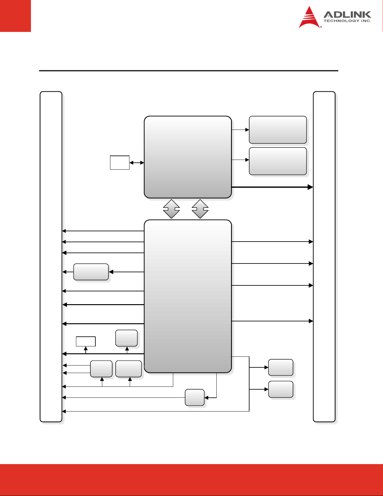
3 Function Diagram
Processor
SODIMM 2
1066/1333 MHz
1~8 GB DDR3
VGA
Dual channel 24-bit LVDS
6x PCIe x1
(port 0~5)
AB
GbE
82579
HD Audio
2x SATA 6 Gb/s (channel 0/1)
2x SATA 3 Gb/s (channel 2/3)
8x USB 2.0 (channel 0/7)
Debug
Header
LPC bus
XDP
SFF26
PCIe x1
(port 7)
TPM
SLB9635
i7 / i5 / i3
Quad & Dual Core
FDI
DMI
PCH
QM67
SODIMM 2
1066/1333 MHz
1~8 GB DDR3
PCI Express x16 (Gen2)
2 x8 or 1x8 + 2x4
DDI 1
DP / HDMI / DVI / SDVO
DDI 2
DP / HDMI / DVI
DDI 3
DP / HDMI / DVI / eDP
PCIe x1
(port 6)
CD
4x GPI
4x GP0
SMBus
GPIO
PCA9535
I2C
SPI
Monitor
ADT7490
BC
SPI 1
BIOS
SPI 2
BIOS
Page 13Express-HR User’s Manual
Page 13Express-IA533 User’s Manual Page 13Express-IA533 User’s ManualExpress-HR User’s Manual Page 13
Page 14
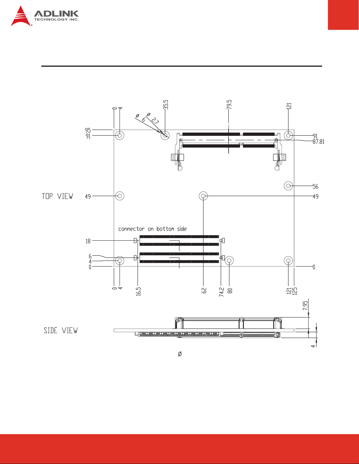
4 Mechanical Dimensions
All tolerances ± 0.05 mm
Other tolerances ± 0.2 mm
Express-HR User’s ManualPage 14
Page 15
5 Pinout and Signal Descriptions
5.1 COM Express® Type 6 compatible pinout
All signals on AB and CD connectors of the Express-HR comply with pinouts and conventions
used in the original “PICMG® COM.0 R2.0: COM Express® Module Base Specification”.
AB Connector
1 Gigabit Ethernet port
LPC and SPI bus
4 Serial A T A channels
High Definition Audio
8 USB 2.0 ports
6 PCI Express Lanes x1
Dual 24-bit LVDS channels
Analog VGA
8 GPIO pins
SMBus and I2C bus
Fan Control Signals
+12V primary power input
+5V standby and 3V RTC
95mm.
125mm.
CD Connector
USB3.0
addtional signals to upgrade
4 USB ports on AB to USB230
2 PCI Express Lanes x1
3 DDI Channels
Displayport/HDMI/DVI and SDVO
PCI Express x16 for Graphics
or General purpose PCIe
CD
AB
The above function mappings are a generic description of COM
Express pinouts, and not necessarily supported on the module
described in this manual.
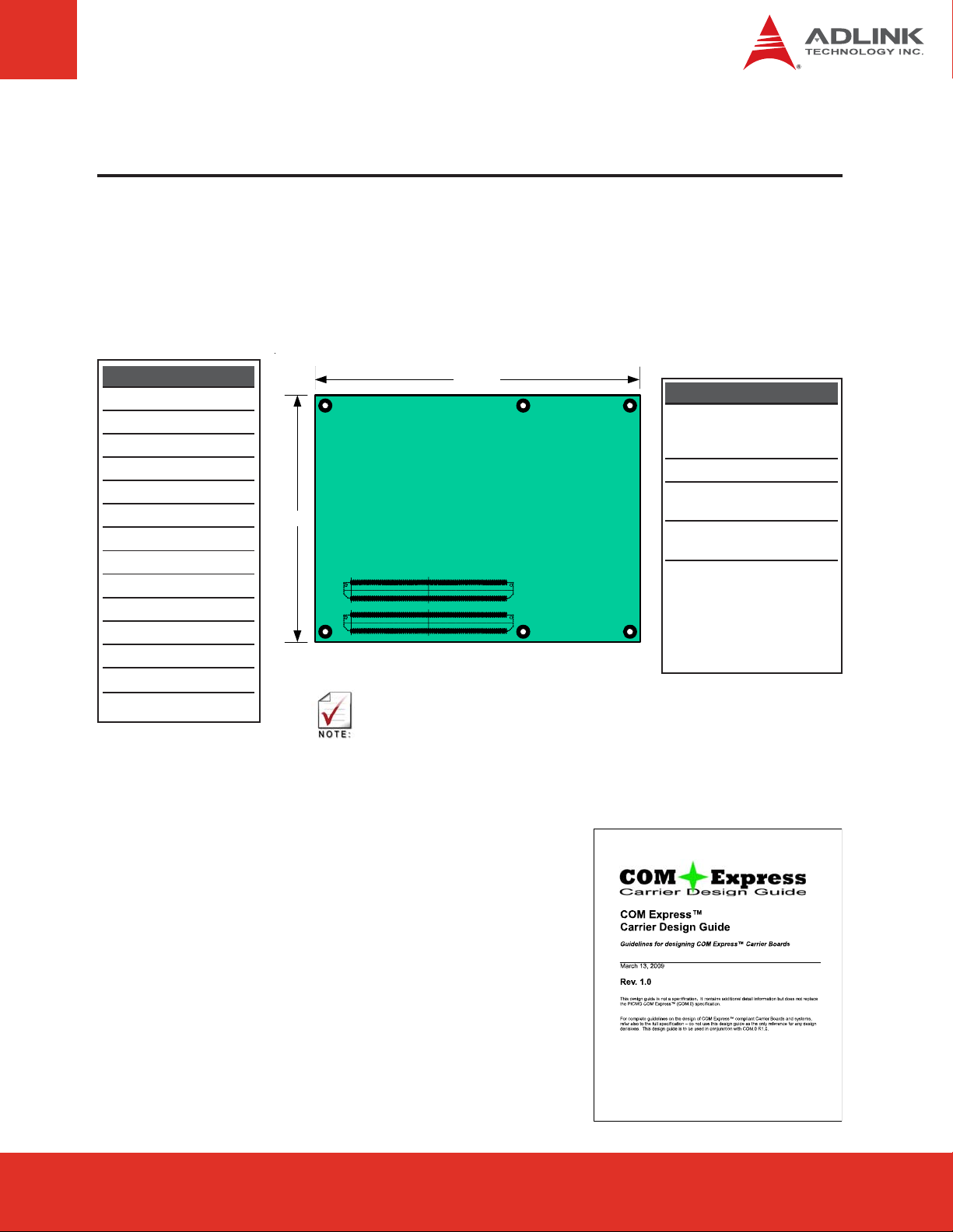
5.2 Carrier Board Design Guide
The PICMG COM Express Carrier Design Guide is a
160-page document that provides information on
designing a custom carrier board for COM Express
modules. The design guide includes reference
schematics for the external circuitry required to
implement the various COM Express peripheral
functions, explains how to extend the supported buses,
and how to add additional peripherals and expansion
slots to a COM Express-based system. You can
download the document Carrier Design Guide at:
http://www.adlinktech.com/ccps/picmg_comdg_100.pdf
Page 15Express-HR User’s Manual
Page 15Express-IA533 User’s Manual Page 15Express-IA533 User’s ManualExpress-HR User’s Manual Page 15
Page 16
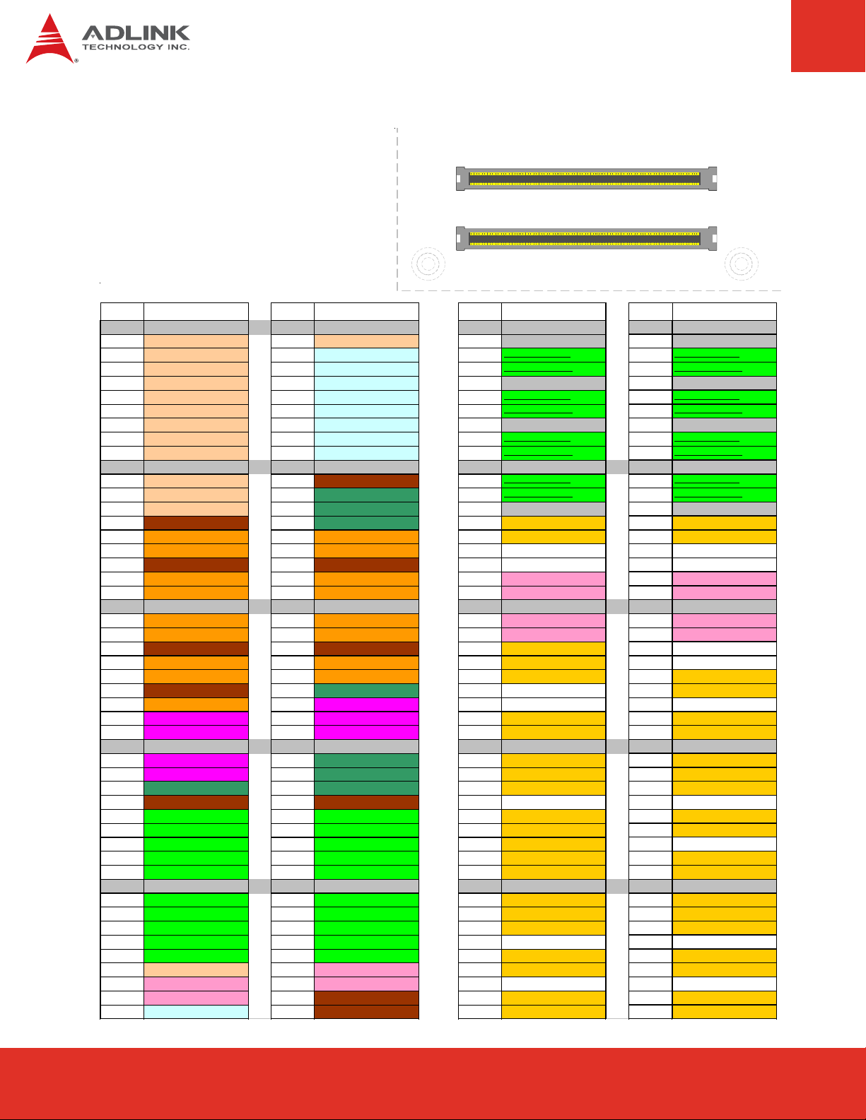
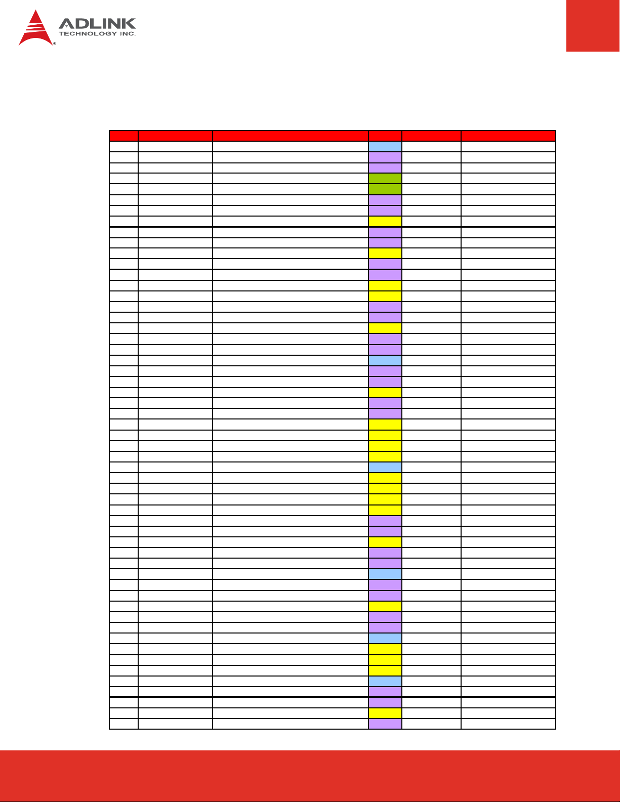
5.3 Pin Definitions
Pinouts for:
D1
D110
C D
C1
C110
B1
COM.0 R2.0 Type 6
A1
B110
A110
A B
Row ARow B Row CRow D
Pi n No. Pi n Nam e Pi n No. Pi n Nam e Pi n No. Pi n Name P i n No . Pin Na me
A1 GND (FIXED) B1 GND (FIXED) C1 GND FIXED) D1 GND FIXED)
A2 GBE0_MDI3- B2 GBE0_ACT#
A3 GBE0_MDI3+ B3 LPC _FRAME#
A4 GBE0_LINK100# B4 LPC_AD0
A5 GBE0_LINK1000# B5 LPC_AD1
A6 GBE0_MDI2- B6 LPC_AD2
A7 GBE0_MDI2+ B7 LPC _AD 3
A8 GBE0_LINK# B8 LPC_DRQ0#
A9 GBE0_MDI1- B9 LPC_DRQ1#
A10 GBE0_MDI1+ B10 LPC_CLK
C2
C3
C4
C5
C6
C7
C8
C9
C10
A11 GND (FIXED) B11 GND (FIXED) C11 GND (FIXED) D11 GND (FIXED)
A12 GBE0_MDI0- B12 PWRBTN#
A13 GBE0_MDI0+ B13 SMB_CK
A14 GBE0_CTREF B14 SMB_DAT
A15 SUS_S3# B15 SMB_ALERT#
A16 SATA0_TX+ B16 SATA1_TX+
A17 SATA0_TX- B17 SATA1_TXA18 SUS_S4# B18 SUS_STAT#
A19 SATA0_RX+ B19 SATA1_RX+
A20 SATA0_RX- B20 SATA1_RX-
C12
C13
C14
C15
C16
C17
C18
C19
C20
A21 GND (FIXED) B21 GND (FIXED) C21 GND (FIXED) D21 GND (FIXED)
A22 SATA2_TX+ B22 SATA3_TX+
A23 SATA2_TX- B23 SATA3_TXA24 SUS_S5# B24 PWR_OK
A25 SATA2_RX+ B25 SATA3_RX+
A26 SATA2_RX- B26 SATA3_RXA27 BATLOW# B27 WDT
A28
A29
A30
(S)ATA_ACT#
AC/HDA_SYNC
AC/HDA_RST#
B28
B29
B30
AC/HDA_SDIN2
AC/HDA_SDIN1
AC/HDA_SDIN0
C22
C23
C24
C25
C26
C27
C28
C29
C30
A31 GND (FIXED) B31 GND (FIXED) C31 GND (FIXED) D31 GND (FIXED)
A32
A33
A34
A35 THRMTRIP# B35 THRM#
A36 USB6- B36 USB7A37 USB6+ B37 USB7+
A38 USB_6_7_OC# B38 USB_4_5_OC#
A39 USB4- B39 USB5A40 USB4+ B40 USB5+
AC/HDA_BITCLK B32 SPKR
AC/HDA_SDOUT B33 I2C_CK
BIOS_DIS0# B34 I2C_DAT
C32
C33
C34
C35
C36
C37
C38
C39
C40
A41 GND (FIXED) B41 GND (FIXED) C41 GND (FIXED) D41 GND (FIXED)
A42 USB2- B42 USB3A43 USB2+ B43 USB3+
A44 USB_2_3_OC# B44 USB_0_1_OC#
A45 USB0- B45 USB1A46 USB0+ B46 USB1+
A47 VCC_RTC B47 EXCD1_PERST#
A48 EXCD0_PERST# B48 EXCD1_CPPE#
A49 EXCD0_CPPE# B49 SYS_RESET#
A50 LPC_SERIRQ B50 CB_RESET#
C42
C43
C44
C45
C46
C47
C48
C49
C50
GND
USB_SSRX0USB_SSRX0+
GND
USB_SSRX1USB_SSRX1+
GND
USB_SSRX2USB_SSRX2+
USB_SSRX3USB_SSRX3+
GND
DDI1_PAI R6+
DDI1_PAI R6RSVD
RSVD
PCIE_RX6+
PCIE_RX6-
PCIE_RX7+
PCIE_RX7DDI1_HPD
DDI1_PAI R4+
DDI1_PAI R4RSVD
RSVD
DDI1_PAI R5+
DDI1_PAI R5-
DDI2_CTRLCLK_AUX+
DDI2_CTRL DATA_AUXDDI2_DDC_AUX_SEL
RSVD
DDI3_CTRLCLK_AUX+
DDI3_CTRL DATA_AUXDDI3_DDC_AUX_SEL
DDI3_PAI R0+
DDI3_PAI R0-
D2
D3
D4
D5
D6
D7
D8
D9
D10
D12
D13
D14
D15
D16
D17
D18
D19
D20
D22
D23
D24
D25
D26
D27
D28
D29
D30
D32
D33
D34
D35
D36
D37
D38
D39
D40
GND
USB_SSTX0USB_SSTX0+
GND
USB_SSTX1USB_SSTX1+
GND
USB_SSTX2USB_SSTX2+
USB_SSTX3USB_SSTX3+
GND
DDI1_CTRLCLK_AUX+
DDI1_CTRL DATA_AUX-
RSVD
RSVD
PCIE_TX6+
PCIE_TX6-
PCIE_TX7+
PCIE_TX7RSVD
RSVD
DDI1_PAIR0+
DDI1_PAIR0RSVD
DDI1_PAIR1+
DDI1_PAIR1-
DDI1_PAIR2+
DDI1_PAIR2-
DDI1_DDC_AUX_SEL
RSVD
DDI1_PAIR3+
DDI1_PAIR3RSVD
DDI2_PAIR0+
DDI2_PAIR0-
DDI3_PAI R1+ D42 DDI2_PAIR1+
DDI3_PAI R1- D43 DDI2_PAIR1DDI3_HPD D44 DDI2_HPD
RSVD D45 RSVD
DDI3_PAI R2+ D46 DDI2_PAIR2+
DDI3_PAI R2- D47 DDI2_PAIR2RSVD D48 RSVD
DDI3_PAI R3+ D49 DDI2_PAIR3+
DDI3_PAI R3- D50 DDI2_PAIR3-
Express-HR User’s ManualPage 16
Page 17
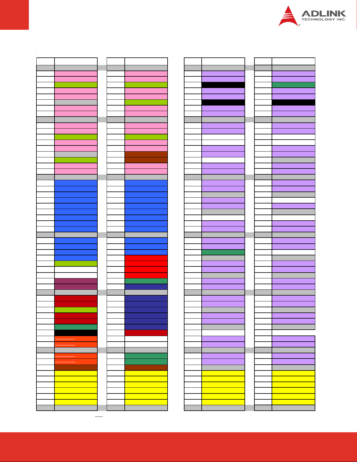
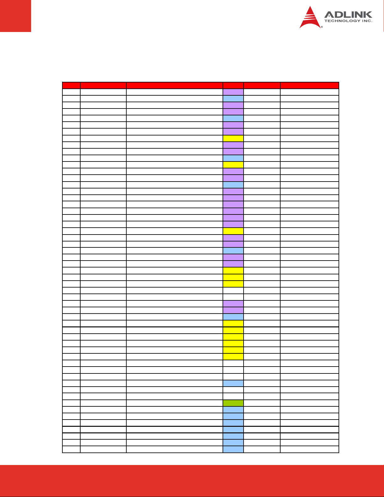
Row DRow A Row B Row C
Pin No. Pin Name Pin No. Pin Na me Pin N o. Pin Name Pin No. Pin Name
A5 1 GND (FIXE D) B 51 GND (FIXED) C51 GND (FIX ED) D51 GND (FIXED )
A52 PCIE_TX5+ B5 2 PCIE_RX5+ C52 PEG_RX0+ D52 PEG_TX0+
A53 PCIE_TX5- B53 PCIE_RX5- C53 PEG_RX0- D53 PEG_TX0A54 GPI0 B54 GPO1 C54 TYPE0# D54 PEG_LANE_RV#
A55 PCIE_TX4+ B55 PCIE_RX4+ C55 PEG_RX1+ D55 PEG_TX1+
A56 PCIE_TX4- B56 PCIE_RX4- C56 PEG_RX1- D56 PEG_TX1A57 GND B57 GPO2 C57 TYPE1# D57 TYPE2#
A58 PCIE_TX3+ B58 PCIE_RX3+ C58 PEG_RX2+ D58 PEG_TX2+
A59 PCIE_TX3- B59 PCIE_RX3- C59 PEG_RX2- D59 PEG_TX2A6 0 GND (FIXE D) B 60 GND (FIXED) C60 GND (FIX ED) D60 GND (FIXED )
A61 PCIE_TX2+ B61 PCIE_RX2+ C61 PEG_RX3+ D61 PEG_TX3+
A62 PCIE_TX2- B62 PCIE_RX2- C62 PEG_RX3- D62 PEG_TX3A63GPI1 B63GPO3 C63RSVD D63RSVD
A64 PCIE_TX1+ B64 PCIE_RX1+ C64 RSV D D64 RSV D
A65 PCIE_TX1- B65 PCIE_RX1- C65 PEG_RX4+ D65 PEG_TX4+
A66 GND B66 WAKE0# C66 PEG_RX4- D66 PEG_TX4A67 GPI2 B67 WAKE1# C67 RSV D D67 GND
A68 PCIE_TX0+ B68 PCIE_RX0+ C68 PEG_RX5+ D68 PEG_TX5+
A69 PCIE_TX0- B69 PCIE_RX0- C69 PEG_RX5- D69 PEG_TX5A7 0 GND (FIXE D) B 70 GND (FIXED) C70 GND (FIX ED) D70 GND (FIXED )
A71 LVDS_A0+ B71 LVDS_B0+ C71 PEG_RX6 + D71 PE G_TX6+
A72 LVDS_A0- B72 LVDS_B0- C72 PEG_RX6- D72 PE G_TX6A73 LVDS_A1+ B73 LVDS_B1+
A74 LVDS_A1- B74 LVDS_B1- C74 PEG_RX7+ D74 PEG_TX7+
A75 LVDS_A2+ B75 LVDS_B2+ C75 PEG_RX7 - D75 PEG_TX7A76 LVDS_A2- B76 LVDS_B2- C76 GND D76 GND
A77 LV DS_VDD_EN B77 LVDS_B3+ C77 RSVD
A78 LVDS_A3+ B78 LVDS_B3- C78 PEG_RX8+ D78 PEG_TX8+
A79 LVDS_A3- B79 LVDS_BKLT_EN C79 PEG_RX8- D79 PEG_TX8A8 0 GND (FIXE D) B 80 GND (FIXED) C80 GND (FIX ED) D80 GND (FIXED )
A81 LVDS_A_CK+ B81 LVD S_B_CK+ C81 PEG_RX9+ D81 PEG_TX9+
A82 LVDS_A_CK- B82 LVDS_B_CK- C8 2 PEG_RX9- D82 PEG_TX9A83 LV DS_I2C_CK B83 LVDS_BKLT_CTRL
A84 LVDS_I2C_DAT B84 VCC_5V_SBY C84 GND D84 GND
A85 GPI3 B85 VCC_5V_SBY C85 PEG_RX10+ D85 PEG_TX10+
A86
A87
A88 PCIE0_CK_REF+
A89 PCIE0_CK_REF- B89 VGA_RED C89 PEG_RX11- D89 PEG_TX11-
A9 0 GND (FIXE D) B 90 GND (FIXED) C90 GND (FIX ED) D90 GND (FIXED )
A91
A92
A93 GPO0 B93 VGA _ HSYNC C93 GND D93 GND
A94
A95
A96
A97
A98
A99
A1 00 G ND (FIXED) B100 GND (FIXE D) C1 00 GND (FI XED ) D100 GND (FIXED )
A101
A102
A103
A104 VCC_12V B10 4 VCC_12V C104 VCC_12V D104 VCC_12V
A105 VCC_12V B10 5 VCC_12V C105 VCC_12V D105 VCC_12V
A106 VCC_12V B10 6 VCC_12V C106 VCC_12V D106 VCC_12V
A107 VCC_12V B10 7 VCC_12V C107 VCC_12V D107 VCC_12V
A108 VCC_12V B10 8 VCC_12V C108 VCC_12V D108 VCC_12V
A109 VCC_12V B10 9 VCC_12V C109 VCC_12V D109 VCC_12V
A1 10 G ND (FIXED) B110 GND (FIXE D) C1 10 GND (FI XED ) D110 GND (FIXED )
RSVD B86 VCC_5V_SBY C86 PEG_RX10- D86 PEG_TX10RSVD B87 VCC_5V_SBY C87 GND D87 GND
SPI_POWER B91 VGA_GRN C91 PEG_RX12+ D91 PEG_TX12+
SPI_MISO B92 VGA_BLU C92 PEG_RX1 2- D92 PEG_TX12-
SPI_CLK B94 VGA_VSYNC C94 PEG_RX1 3+ D94 PEG_TX13+
SPI_MOSI B95 VGA_I2C_CK C95 PEG_RX13- D95 PEG_TX13-
TPM_PP B96 VGA_I2C_DAT C96 GND D96 GND
TYPE10#
SER0_TX
SER0_RX
SER1_TX
SER1_RX
LID#
B88
B97
B98
B99
B101
B102
B103
BIOS_DIS 1 # C8 8 PEG_RX1 1+ D88 PEG_TX11+
SPI_CS# C97 RSV D
RSVD C98 PEG_RX14+ D98 PEG_TX14+
RSVD C99 PEG_RX14- D99 PEG_TX14-
FAN_PWMOUT C101 PEG_RX15+ D101 PEG_TX15+
FAN_TA CHIN C102 PEG_RX15- D102 PEG_TX15-
SLEEP# C103 GND D103 GND
XXX Strikethrough pin names indicates that the signal is not supported on this module.
C73
C83
GND
TPM_PP D83 RSVD
D73
D77
D97
GND
RSVD
RSVD
Page 17Express-HR User’s Manual
Page 17Express-IA533 User’s Manual Page 17Express-IA533 User’s ManualExpress-HR User’s Manual Page 17
Page 18
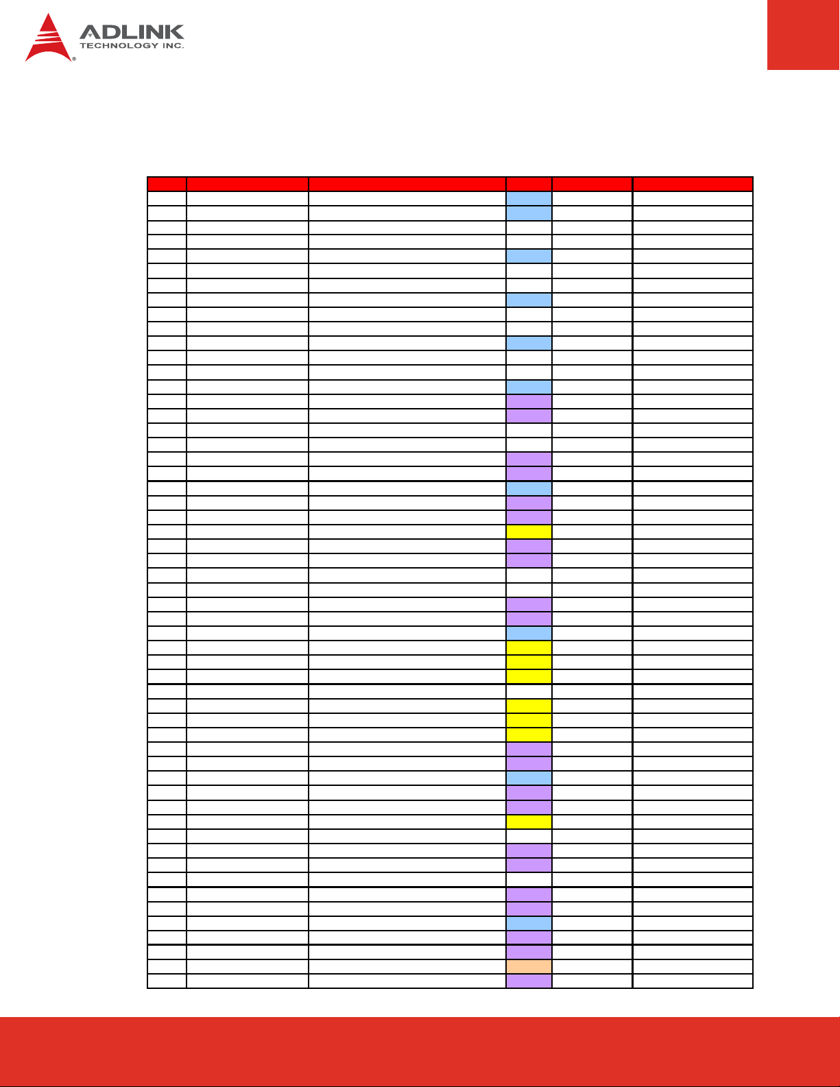
5.4 Signal Descriptions
Pin Signal Description Type PU/PD Comment
A1 GND Ground PWR - A2 GBE0_MDI3- Ethernet Media Dependent Interface - I/O - DP - A3 GBE0_MDI3+ Ethernet Media Dependent Interface + I/O - DP - A4 GBE0_LIN K100# Ethe rnet Speed LED (100Mb) OD - On at 100Mb/s
A5 GBE0_LINK1000 # Ethernet Speed LED (1000Mb) OD - On at 1000Mb/s
A6 GBE0_MDI2- Ethernet Media Dependent Interface - I/O - DP - A7 GBE0_MDI2+ Ethernet Media Dependent Interface + I/O - DP - A8 GBE0_LI NK# LAN Link LED O-3.3 -
A9 GBE0_MDI1- Ethernet Media Dependent Interface - I/O - DP - A10 GBE0_MDI1+ Ethernet Media Dependent Interface + I/O - DP - A11 GND Ground PWR - A12 GBE0_MDI0- Et hernet Media Dependent Interface - I/O - DP - A13 GBE0_MDI0+ Ethernet Media Dependent Interface + I/O - DP - A14 GBE0_CTREF ETHCTREF O-1,8 - A15 SUS_S3# PM_SLP _S#3 O-3.3 - A16
A17
A18
A19
A20
A21
A22
A23
A24
A25
A26
A27
A28
A29
A30
A31
A32
A33
A34
A35
A36
A37
A38
A39
A40
A41
A42
A43
A44
A45
A46
A47
A48
A49
A50
A51
A52
A53
A54
A55
SATA0_TX+
SATA0_TX-
SUS_S4#
SATA0_RX+
SATA0_RX-
GND
SATA2_TX+
SATA2_TX-
SUS_S5#
SATA2_RX+
SATA2_RX-
BATLOW#
ATA_ACT#
AC_SYNC
AC_RST#
GND
AC_BITCLK
AC_SDOUT
BIOS_DISABLE#
THRMTR IP#
USB6-
USB6+
USB_6_7_OC#
USB4-
USB4+
GND
USB2-
USB2+
USB_2_3_OC#
USB0-
USB0+
VCC_RTC
EXCD0_PER ST#
EXCD0_CPPE#
LPC_SERIRQ
GND
PCIE5_TX+
PCIE5_TX-
GPI0
PCIE4_TX+
SATA0_TX+ | SATA 0 Transmi t Data + O - DP - SATA0_TX- | SATA 0 Transmit Data - O - DP - PM_SLP_S#4 O-3.3 - SATA0_RX+ | SATA 0 Receive Data + I - DP - SATA0_RX - | SATA 0 Receive Data - I - DP - Ground PWR - SATA2_TX+ | SATA 2 Transmi t Data + O - DP - SATA2_TX- | SATA 2 Transmit Data - O - DP - PM_SLP_S#5 O-3.3 - SATA2_RX+ | SATA 2 Receive Data + I - DP - SATA2_RX- | SATA 2 Recei ve Data - I - DP - PM_BATLOW# | Battery Low I-3.3 PU 8k2 3.3Vsb ATA_LED# | SATA LED O-3.3 PU 10k 3.3V
AC_SYNC | AC'97 Sync O-3 .3 - int. PD 20k in QM57
AC_RST# | AC'97 Reset O-3.3 - int. PD 20k in QM5 7
Ground PWR AC_BITCLK | AC'97 Clock O-3.3 - int. PD 20k in QM57
AC_S D A TA O UT | AC '9 7 Da ta O-3 .3 - int . PD 20k in QM 57
BIOS_DISABLE# I-3.3 PU 10k 3.3Vsb PM_THRMTRIP#_CON O-3 .3 PU 33 0 3.3V USB_PN6 | USB Data – Port6 I/O - DP - int. PD 20k in QM57
USB_PP6 | USB Data + Por t6 I / O - DP - int. PD 20k in QM57
USB_OC#_6_7 | USB OverCurrent Port 6/ 7 I-3.3 PU 10k 3.3Vsb USB_PN4 | USB Data - Port4 I/O - DP - int. PD 20k in QM57
USB_PP4 | USB Data + Por t4 I / O - DP - int. PD 20k in QM57
Ground PWR - USB_PN2 | USB Data - Port2 I/O - DP - int. PD 20k in QM57
USB_PP2 | USB Data + Por t2 I / O - DP - int. PD 20k in QM57
USB_OC#_2_3 | USB OverCurrent Port 2/ 3 I-3.3 PU 10k 3.3Vsb
USB_PN0 | USB Data - Port0 I/O - DP - int. PD 20k in QM57
USB_PP0 | USB Data + Por t0 I / O - DP - int. PD 20k in QM57
V_BAT PWR - Express Card Suppo rt [0 ]|card reset O- 3.3 PU 10k 3.3 Vsb Express Card Support [0]| capable request I-3.3 PU 10k 3.3V INT_S ER IRQ | Serial In terrupt Requ est IO-3. 3 PU 10k 3. 3V Ground PWR - PCI Express 5 Transmit + O - DP - PCI Express 5 Transmit - O - DP - General Purpose Input 0 I-3.3 PU 10k 3.3Vsb PCI Express 4 Transmit + O - DP - -
Row A
Express-HR User’s ManualPage 18
Page 19
Signal Descriptions (cont’d)
Row A
Pin Signal Description Type PU/PD Comment
A56
A57
A58
A59
A60
A61
A62
A63
A64
A65
A66
A67
A68
A69
A70
A71
A72
A73
A74
A75
A76
A77
A78
A79
A80
A81
A82
A83
A84
A85
A86
A87
A88
A89
A90
A91
A92
A93
A94
A95
A96
A97
A98
A99
A100
A101
A102
A103
A104
A105
A106
A107
A108
A109
A110
PCIE4_TX-
GND
PCIE3_TX+
PCIE3_TX-
GND
PCIE2_TX+
PCIE2_TX-
GPI1
PCIE1_TX+
PCIE1_TX-
GND
GPI2
PCIE0_TX+
PCIE0_TX-
GND
LVDS_A0+
LVDS_A0-
LVDS_A1+
LVDS_A1-
LVDS_A2+
LVDS_A2-
LVDS_VDD_EN
LVDS_A3+
LVDS_A3-
GND
LVDS_A_CK+
LVDS_A_CK-
LVDS_I2C_CK
LVDS_I2C_DAT
GPI3
RSVD
RSVD
PCIE_CK_REF+
PCIE_CK_REF-
GND
SPI_POWER
SPI_MISO
GPO0
SPI_CLK
SPI_MOSI
TPM_PP
TYPE10#
SER0_T X
SER0_RX
GND
SER1_T X
SER1_RX
LID#
VCC_12V
VCC_12V
VCC_12V
VCC_12V
VCC_12V
VCC_12V
GND
PCI Express 4 Transmit - O - DP - Ground PWR - PCI Express 3 Transmit + O - DP - PCI Express 3 Transmit - O - DP - Ground PWR - PCI Express 2 Transmit + O - DP - PCI Express 2 Transmit - O - DP - General Purpose Input 1 I-3.3 PU 10k 3.3Vsb PCI Express 1 Transmit + O - DP - PCI Express 1 Transmit - O - DP - Ground PWR - General Purpose Input 2 I-3.3 PU 10k 3.3Vsb PCI Express 0 + O - DP - PCI Express 0 - O - DP - Ground PWR - LVDS_AP0 | LVDS Chann el A O - DP - LVDS_AN0 | LVDS Channel A O - DP - LVDS_AP1 | LVDS Chann el A O - DP - LVDS_AN1 | LVDS Channel A O - DP - LVDS_AP2 | LVDS Chann el A O - DP - LVDS_AN2 | LVDS Channel A O - DP - LVDS_VDDEN | LVDS Panel Power O-2,5 PD 10k LVDS_AP3 | LVDS Chann el A O - DP - LVDS_AN3 | LVDS Channel A O - DP - Ground PWR - LVDS_CLKAP | LVDS Channel A O - DP - LVDS_CLKAN | LVDS Channel A O - DP - LVDS_DDCPCLK | JILI I2C Clock IO-3.3 PU 2k 2 3. 3V LVDS_DDCPDATA | JILI I2C Data IO-3.3 PU 2k2 3. 3V General Purpose Input 3 I-3.3 PU 10k 3.3Vsb NC NC NC NC CLK_PCI E_REF P O - DP - CLK_PCI E_REF N O - DP - Ground PWR - Power supply for Carr i er Board SPI O-3.3 - -
IO - General Purpose Output 0 O-3.3 PU 10k 3.3Vsb Clock from Module to Carrier SPI IO - Data out from Module to Carrier SPI IO - Trus te d P l atform Module IO-3.3 - Module type ID pin 10 NC - serial port transmitter NC - seri a l port re ceiver NC - Ground PWR - serial port transmitter NC - seri a l port re ceiver NC - LID button.
Power 12V PWR - Power 12V PWR - Power 12V PWR - Power 12V PWR - Power 12V PWR - Power 12V PWR - Ground PWR - -
OD
--
Page 19Express-HR User’s Manual
Page 19Express-IA533 User’s Manual Page 19Express-IA533 User’s ManualExpress-HR User’s Manual Page 19
Page 20
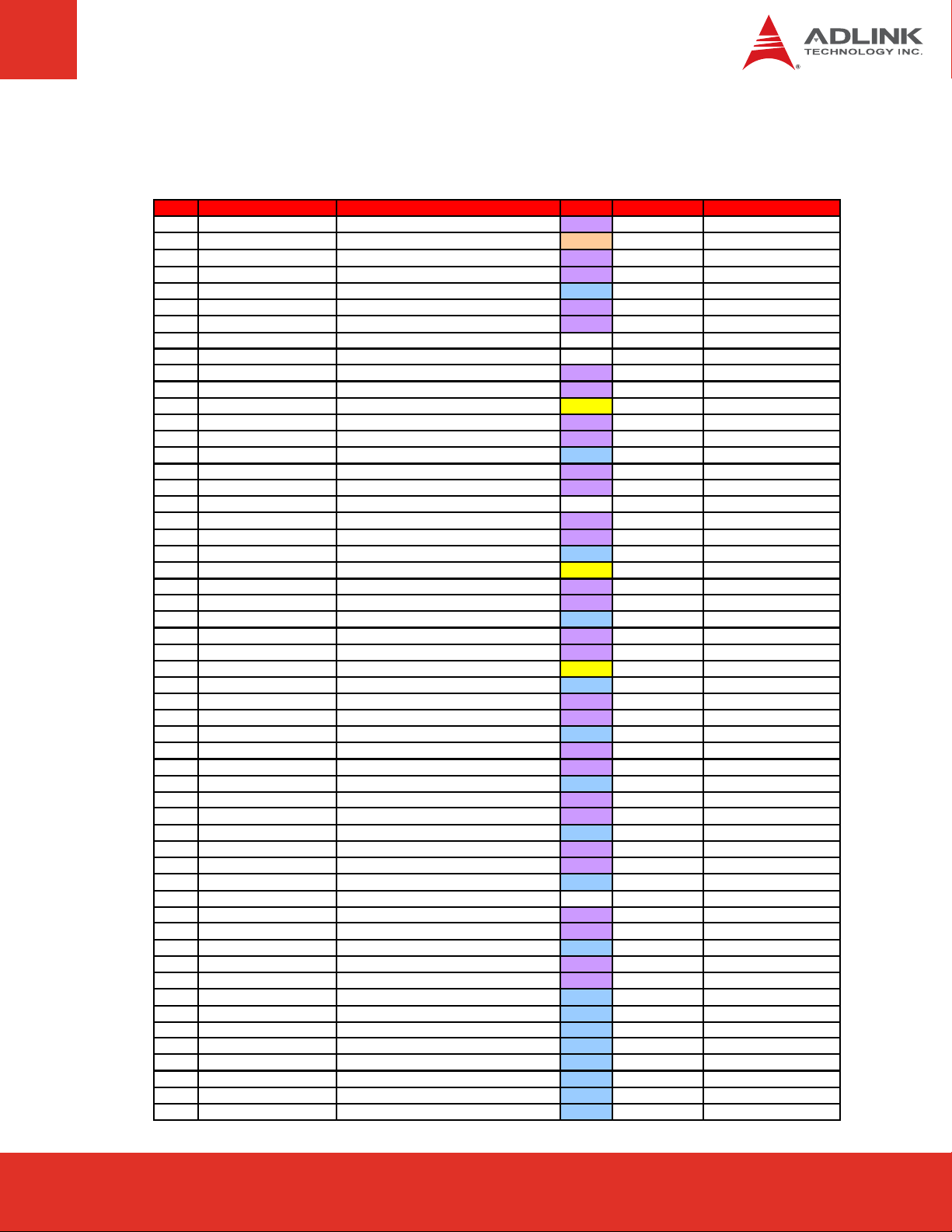
Signal Descriptions (cont’d)
Row B
Pin Signal Description Type PU/PD Comment
B1 GND Ground PWR - B2 GBE0_ACT# LAN_ACTLE D# | Et hernet Acti vi ty LED OD PU 1k 3. 3V B3 LPC_FRAME# LPC_FRAME# | LPC Frame Ind icator O-3.3 - B4 LPC_AD0 LPC_AD0 | LPC Adr ess & DATA Bus I O-3.3 B5 LPC_AD1 LPC_AD1 | LPC Adr ess & DATA Bus I O-3.3 B6 LPC_AD2 LPC_AD2 | LPC Adr ess & DATA Bus I O-3.3 B7 LPC_AD3 LPC_AD3 | LPC Adr ess & DATA Bus I O-3.3 B8 L PC_DRQ0# SIO_DR Q#0 | LPC Se ri al DMA Request 0 I -3.3 - int. PU 20k in QM57
B9 L PC_DRQ1# SIO_DR Q#1 | LPC Se ri al DMA Request 1 I -3.3 - int. PU 20k in QM57
B10 LPC_CLK CLK_SIOEXTPCI O-3.3 - B11 GND Ground I-3.3 - B12 PWR BTN# Power Button I-5 PU 10k 3.3Vsb B13 SMB_CK SMBUS Clo ck O-3 .3 PU 2k 2 3.3 V sb B14 SMB_DAT SMBUS Data IO-3. 3 PU 2k2 3.3Vsb B15 SM B _A L ER T # SMB _A LER T # I-3.3 PU 10 k 3.3V sb B16
B17
B18
B19
B20
B21
B22
B23
B24
B25
B26
B27
B28
B29
B30
B31
B32
B33
B34
B35
B36
B37
B38
B39
B40
B41
B42
B43
B44
B45
B46
B47
B48
B49
B50
B51
B52
B53
B54
B55
SATA1_TX+
SATA1_T XSUS_STAT#
SATA1_RX+
SATA1_RX-
GND
SATA3_TX+
SATA3_T X-
PWR_OK
SATA3_RX+
SATA3_RX-
WDT
AC_SDIN2
AC_SDIN1
AC_SDIN0
GND
SPKR
I2C_CK
I2C_DAT
THRM#
USB7-
USB7+
USB_4_5_OC#
USB5-
USB5+
GND
USB3-
USB3+
USB_0_1_OC#
USB1-
USB1+
EXCD1_PER ST#
EXCD1_CPPE#
SYS_RESE T#
CB_RESET#
GND
PCIE5_RX+
PCIE5_RX-
GPO1
PCIE4_RX+
SATA1_TX+ | SATA 1 Transmi t Data + O - DP - SATA1_TX- | SATA 1 Transmit Data - O - DP - PM_S U S _ ST A T# O-3 .3 - SATA1_RX+ | SATA 1 Receive Data + I - DP - SATA1_RX - | SATA 1 Receive Data - I - DP - Ground PWR - SATA3_TX+ | SATA 3 Transmi t Data + O - DP - SATA3_TX- | SATA 3 Transmit Data - O - DP - Po w er OK I,3.3 PU 10k 3.3Vsb SATA3_RX+ | SATA 3 Receive Data + I - DP - SATA3_RX - | SATA 3 Receive Data - I - DP - Watch Dog Timer O-3.3 AC_SDATAIN2 I-3.3 - int. PD 20k in QM57
AC_SDATAIN1 I-3.3 - int. PD 20k in QM57
AC_SDATAIN0 I-3.3 - int. PD 20k in QM57
Ground PWR AC_SPK R O-3.3 - i nt . PD 20k in QM57
I2C L K O-3 .3 PU 10k 3.3V I2 D A T IO-3.3 PU 10 k 3 .3V PM THRM # CO N | Over Tempera t ure I -3.3 USB_PN7 | USB Data – Port7 I/O - DP - int. PD 20k in QM57
USB_PP 7 | USB Data + Port7 I/O - DP - int. PD 20k in QM57
USB_OC#_4_5 | USB OverCurrent Port I-3.3 PU 10k 3.3Vsb
USB_PN5 | USB Data- Port5 I/O - DP - int. PD 20k in QM57
USB_PP 5 | USB Data+ Port5 I/O - DP - int . PD 20k in QM57
Ground I-3.3 - USB_PN3 | USB Data- Port3 I/O - DP - int. PD 20k in QM57
USB_PP 3 | USB Data+ Port3 I/O - DP - int . PD 20k in QM57
USB_OC#_0_1 | USB OverCurrent Port I-3.3 PU 10k 3.3Vsb USB_PN1 | USB Data- Port1 I/O - DP - int. PD 20k in QM57
USB_PP 1 | USB Data+ Port1 I/O - DP - int . PD 20k in QM57
Express Card Support [1]|card reset O-3.3 P U 10k 3.3Vsb Express Card Support [1]| capable c. I-3.3 PU 10k 3.3V ETX_SYS_RESET# | Reset Input I-3. 3 Pull up +3.3V internally
PCI_ RS T # | PCI B us Reset O-3 .3 - Ground PWR - PCI Ex press 5 Reciev e + I - DP - PCI Ex press 5 Receiv e - I - DP - Gene r a l Pu rp os e O ut pu t 1 O-3 .3 PU 10 k 3.3 V sb PCI Ex press 4 Reciev e + I - DP - -
Express-HR User’s ManualPage 20
Page 21
Signal Descriptions (cont’d)
Row B
Pin Signal Description Type PU/PD Comment
B56
B57
B58
B59
B60
B61
B62
B63
B64
B65
B66
B67
B68
B69
B70
B71
B72
B73
B74
B75
B76
B77
B78
B79
B80
B81
B82
B83
LVDS_BKLT_CTRL
B84
B85
B86
B87
B88
B89
B90
B91
B92
B93
B94
B95
B96
B97
B98
B99
B100
B101
B102
B103
B104
B105
B106
B107
B108
B109
B110
PCIE4_RX-
GPO2
PCIE3_RX+
PCIE3_RX-
GND
PCIE2_RX+
PCIE2_RX-
GPO3
PCIE1_RX+
PCIE1_RX-
WAKE0#
WAKE1#
PCIE0_RX+
PCIE0_RX-
GND
LVDS_B0+
LVDS_B0-
LVDS_B1+
LVDS_B1-
LVDS_B2+
LVDS_B2-
LVDS_B3+
LVDS_B3-
LVDS_BKLT_EN
GND
LVDS_B_CK+
LVDS_B_CK-
VCC_5V_ SBY
VCC_5V_ SBY
VCC_5V_ SBY
VCC_5V_ SBY
BIOS_DS1#
VGA_RED
GND
VGA_GRN
VGA_BLU
VGA_HSYNC
VGA_VSYNC
VGA_I2C_CK
VGA_I2C_DAT
SPI_CS#
RSVD
RSVD
GND
FAN_PWMOUT
FAN_TACHIN
SLEEP#
VCC_12 V
VCC_12 V
VCC_12 V
VCC_12 V
VCC_12 V
VCC_12 V
GND
PCI Ex press 4 Receiv e - I - DP - Gene r a l Pu rp os e O ut pu t 2 O-3 .3 PU 10 k 3.3 V sb PCI Ex press 3 Reciev e + I - DP - PCI Ex press 3 Receiv e - I - DP - Ground PWR - PCI Ex press 2 Receiv e + I - DP - PCI Ex press 2 Receiv e - I - DP - Gene r a l Pu rp os e O ut pu t 3 O-3 .3 PU 10 k 3.3 V sb PCI Ex press 1 Receiv e + I - DP - PCI Ex press 1 Receiv e - I - DP - PCIE_WAKEI# I-3.3 PU 1k 3.3Vsb WAKE1# I-3.3 PU 10k 3.3Vsb PCI Ex press 0 Receiv e + I - DP - PCI Ex press 0 Receiv e - I - DP - Ground PWR - LVDS_BP0 | LVDS Chann el B Data0+ O - DP - LVDS_BN0 | LVDS Channel B Data0- O - DP - LVDS_BP1 | LVDS Chann el B Data1+ O - DP - LVDS_BN1 | LVDS Channel B Data1- O - DP - LVDS_BP2 | LVDS Chann el B Data2+ O - DP - LVDS_BN2 | LVDS Channel B Data2- O - DP - LVDS_BP3 | LVDS Chann el B Data3+ O - DP - LVDS_BN3 | LVDS Channel B Data3- O - DP - LVDS Panel Backlight Enable O-3.3 PD 100k Ground PWR - LVDS_CLKBP | LVDS Channel B O - DP - LVDS_CLKBM | LVDS Channel B O - DP - Ba ck lig ht Brightne ss O-3 .3 PD 100k 5V Standby PWR - 5V Standby PWR - 5V Standby PWR - 5V Standby PWR - Selection straps to determine BIOS boot device I-3.3 - Analog V ideo RGB-RED OA PD 150R Ground PWR - Analog V ideo RGB-GREEN OA PD 150R Analog V ideo RGB-BLUE OA PD 150R Analog V ideo H-Sync O-3.3 - Analog Video V-Sync O-3.3 - Display Data Channel - Clock O-3.3 Display Data Channel - Data IO-3. 3 Chip select for Carrier Board SPI O-3.3 - NC
NC
Ground PWR - Fan speed control. O-3.3 - Fan tachometer input forfan with 2 pulse output I-3.3 - Sleep button. I-3.3 - Power 12V PWR - Power 12V PWR - Power 12V PWR - Power 12V PWR - Power 12V PWR - Power 12V PWR - Ground PWR - -
NC
NC
--
--
Page 21Express-HR User’s Manual
Page 21Express-IA533 User’s Manual Page 21Express-IA533 User’s ManualExpress-HR User’s Manual Page 21
Page 22
Signal Descriptions (cont’d)
Row C
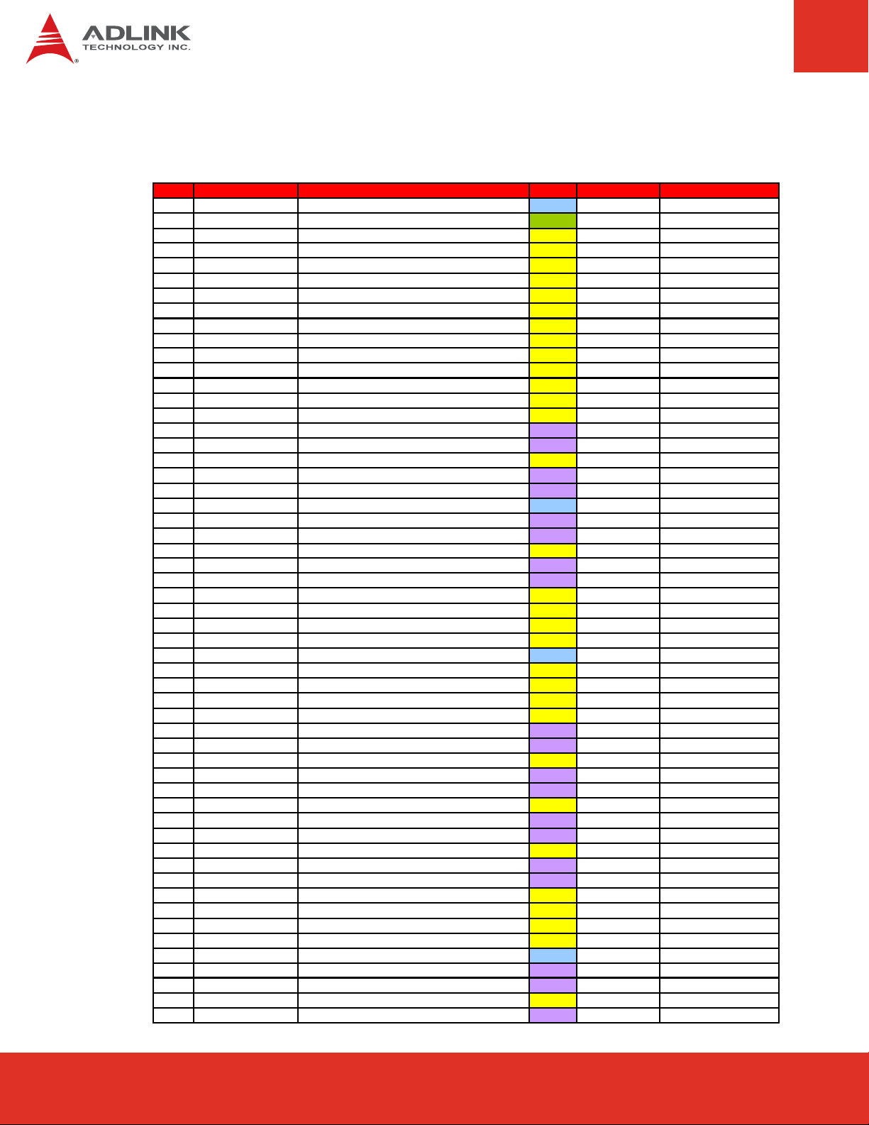
Pin Signal Description Type PU/PD Comment
C1
C2
C3
C4
C5
C6
C7
C8
C9
C10
C11
C12
C13
C14
C15
C16
C17
C18
C19
C20
C21
C22
C23
C24
C25
C26
C27
C28
C29
C30
C31
C32
C33
DDI 2_CTRLDATA_AUX - DP2_AUX- / HDMI2_CT RLDATA
C34
C35
C36
DDP3_CTRLCLK_AUX+
C37
DDP3_ CTRLCLK_AUX- DP3 AUX- / HDMI 3 CTRL DATA
C38
C39
C40
C41
C42
C43
C44
C45
C46
C47
C48
C49
C50
C51
C52
C53
C54
C55
GND
GND
USB_SSRX0-
USB_SSRX0+
GND
USB_SSRX1-
USB_SSRX1+
GND
USB_SSRX2-
USB_SSRX2+
GND
USB_SSRX3-
USB_SSRX3+
GND
DDI_PAIR6+
DDI_ PAIR6- SDVO1_FLDSTALL-
RSVD
RSVD
PCIE_RX6+
PCIE_RX6-
GND
PCIE_RX7+
PCIE_RX7-
DDI1_HPD DP1 /HDMI1 Ho t-Plug D etect
DDI1_PAIR4+ SDVO1_INT+
DDI1_PAIR4- SDVO1_INT-
RSVD
RSVD
DDI1_PAIR5+
DDI1_PAIR5- SDVO1_TVCLKIN-
GND Ground
DDI2 _CTRLCLK_A UX+ DP2_AUX + / HD MI2_CTRLCLK
DDI2_DDC_AUX_SEL DP2 and HDMI2 Select mode
RSVD
DDI3_DDC_AUX_SEL DP3 and HDMI3 Select mode
DDI3_PAI R0+ DP3_LANE0+ / TMDS3_DA TA2+
DDI3_PAI R0- DP3_LANE0- / TMDS3_DATA2-
GND Ground
DDI3_PAIR1+
DDI3_PAIR1-
DDI3_HPD DP3 /HDMI3 Ho t-Plug D etect
RSVD
DDI3_PAI R2+ DP3_LANE2+ / TMDS3_DA TA0+
DDI3_PAI R2- DP3_LANE2- / TMDS3_DATA0-
RSVD
DDI3_PAIR3+
DDI3_PAIR2-
GND Ground
PEG_RX0+ P CIe 0 Recieve +
PEG_RX0- P CIe 0 Recieve -
TYPE0# Module type I D pin 0
PEG_RX1+ P CIe 1 Recieve +
Ground PWR - Ground PWR -
NC - NC - -
Ground PWR - -
NC - NC - -
Ground PWR - -
NC - NC - -
Ground PWR - -
NC - -
NC Ground PWR SDVO1_FLDSTALL+
PCI Express 6 Receive + O - DP PCI Express 6 Receive - O - DP
Ground
PCI Express 7 Receive + O - DP PCI Express 7 Receive - O - DP - -
SDVO1_TVCLKIN+
DP3 AUX+ / HDMI3 CTRLC LK
DP3_LANE1+ / TMDS3_DATA1+
DP3_LANE1- / TMD S3_DATA1-
DP3_LANE3+ / TMDS3_CLK+
DP3_LANE3- / TMD S3_CLK-
O - DP
O - DP
NC -
NC
PWR -
I-3.3 - O - DP - O - DP - -
NC - -
NC - O - DP - O - DP - -
PWR - IO-3.3 - IO-3.3 - IO-3.3 -
NC IO-3.3 IO-3.3 IO-3.3 -
O - DP - O - DP - -
PWR - O - DP - O - DP - -
IO-3.3 - -
NC - O - DP - O - DP - -
NC O - DP O - DP -
PWR I - DP I - DP - -
STO - not co nn e cte d
I - DP - -
Express-HR User’s ManualPage 22
Page 23
Signal Descriptions (cont’d)
Row C
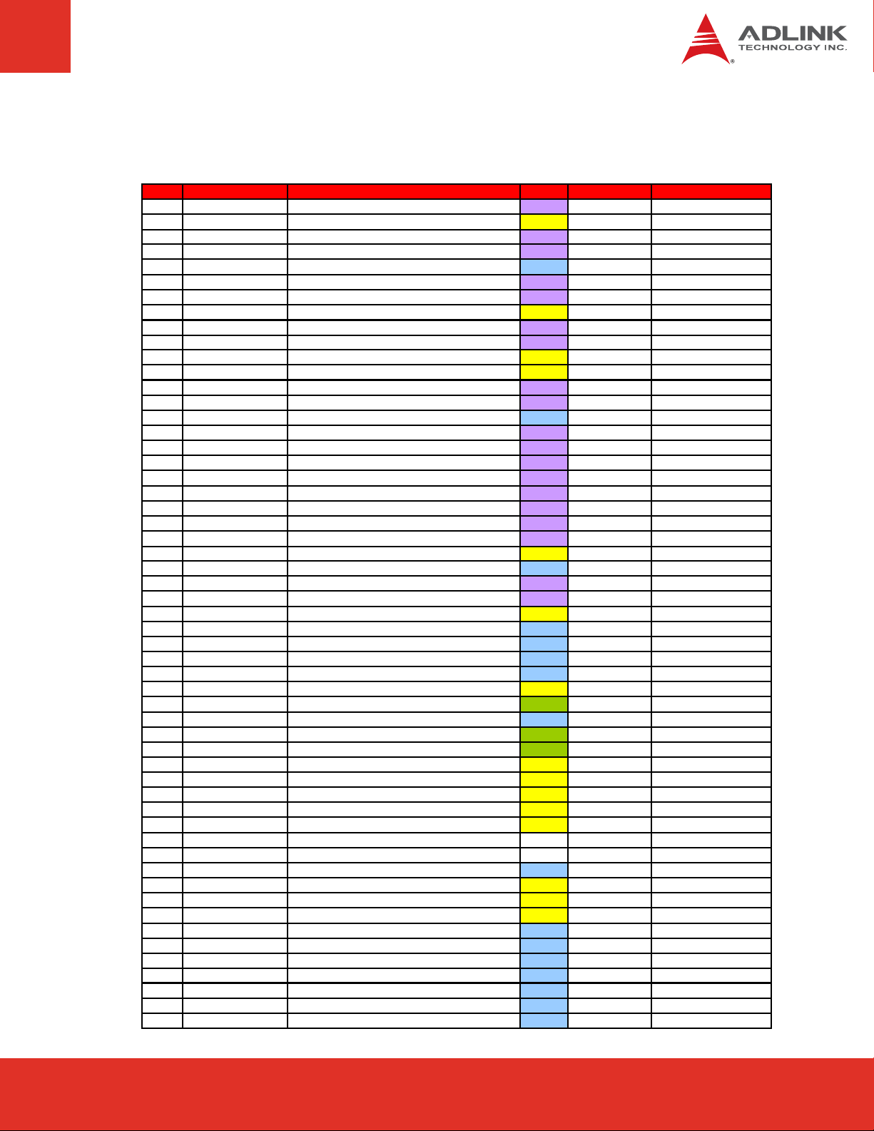
Pin Signal Description Type PU/PD Comment
C56
C57
C58
C59
C60
C61
C62
C63
C64
C65
C66
C67
C68
C69
C70
C71
C72
C73
C74
C75
C76
C77
C78
C79
C80
C81
C82
C83
C84
C85
C86
C87
C88
C89
C90
C91
C92
C93
C94
C95
C96
C97
C98
C99
C100
C101
C102
C103
C104
C105
C106
C107
C108
C109
C110
PEG_RX1 -
TYPE1# Module type I D pi n 1
PEG_RX2+ P CIe 2 Recieve +
PEG_RX2- P CIe 2 Recieve -
GND Ground
PEG_RX3+
PEG_RX3- P CIe 3 Recieve -
RSVD
RSVD
PEG_RX4+ P CIe 4 Recieve +
PEG_RX4- P CIe 4 Recieve -
RSVD FAN_PWM_CTRL
PEG_RX5+
PEG_RX5- P CIe 5 Recieve -
GND Ground
PEG_RX6+ P CIe 6 Recieve +
PEG_RX6- P CIe 6 Recieve -
RSVD NC NC
PEG_RX7+
PEG_RX7 -
GND Ground
RSVD FA N_TACH
PEG_RX8+ P CIe 8 Recieve +
PEG_RX8- P CIe 8 Recieve -
GND Ground
PEG_RX9+
PEG_RX9 -
RSVD Phys i ca l Pr es ence
GND Ground
PEG_RX10+ PCIe 10 Recieve +
PEG_RX10- PCIe 10 Recieve -
GND Ground
PEG_RX11+
PEG_RX11-
GND Ground
PEG_RX12+ PCIe 12 Recieve +
PEG_RX12- PCIe 12 Recieve -
GND Ground
PEG_RX13+ PCIe 13 Recieve +
PEG_RX13-
GND
RSVD NC NC
PEG_RX14+ PCIe 14 Recieve +
PEG_RX14- PCIe 14 Recieve -
GND Ground
PEG_RX15+ PCIe 15 Recieve +
PEG_RX15-
GND
VCC_12V
VCC_12V
VCC_12V
VCC_12V
VCC_12V
VCC_12V
GND
PCIe 1 Recieve -
PCIe 3 Recieve +
NC NC - NC NC - -
PCIe 5 Recieve +
PCIe 7 Recieve +
PCIe 7 Recieve -
PCIe 9 Recieve +
PCIe 9 Recieve -
PCIe 11 Recieve +
PCIe 11 Recieve –
PCIe 13 Recieve Ground
PCIe 15 Recieve Ground
Power 12V PWR - Power 12V PWR - Power 12V PWR - Power 12V PWR - Power 12V PWR - Power 12V PWR - Ground
I - DP - -
STO - not co nn e cte d
I - DP - I - DP - -
PWR - I - DP - I - DP - -
I - DP - I - DP - -
0-5 - I - DP - I - DP - -
PWR - I - DP - I - DP - -
-I - DP - I - DP - -
PWR - -
I-5 - I - DP - I - DP - -
PWR - I - DP - I - DP - -
I-3.3
PU 10k 3.3 V sb
PWR - I - DP - I - DP - -
PWR - I - DP - I - DP - -
PWR - I - DP - I - DP - -
PWR - I - DP - I - DP - -
PWR - -
-I - DP - I - DP - -
PWR - I - DP - I - DP - -
PWR - -
PWR - -
-
Page 23Express-HR User’s Manual
Page 23Express-IA533 User’s Manual Page 23Express-IA533 User’s ManualExpress-HR User’s Manual Page 23
Page 24

Signal Descriptions (cont’d)
Row D
Pin Signal Description Type PU/PD Comment
D1
D2
D3
D4
D5
D6
D7
D8
D9
D10
D11
D12
D13
D14
D15
DDP1 _CTRLCLK_AUX+
D16
DDP1_CTRLDATA_AUX- DP1 AUX- / HDMI1/SDVO1_CTRLDATA
D17
D18
D19
D20
D21
D22
D23
D24
D25
D26
D27
D28
D29
D30
D31
D32
D33
D34
D35
D36
D37
D38
D39
D40
D41
D42
D43
D44
D45
D46
D47
D48
D49
D50
D51
D52
D53
D54
D55
GND
GND
USB_SSTX0-
USB_SSTX0+
GND
USB_SSTX1-
USB_SSTX1+
GND
USB_SSTX2-
USB_SSTX2+
GND
USB_SSTX3-
USB_SSTX3+
GND
RSVD
RSVD
PCIE_TX6+
PCIE_TX6-
GND
PCIE_TX7+
PCIE_TX7-
RSVD
RSVD
DDI1_PAIR0+
DDI1_PAIR0-
RSVD
DDI1_PAIR1+
DDI1_PAIR1-
GND
DDI1_PAIR2+
DDI1_PAIR2-
DDI1_ DDC_AUX_SEL DP1 and HDMI1 Select m ode
RSVD
DDI1_PAIR3+ DP1_LANE3+ / TMDS1_CLK+ / SDVO1_CK+
DDI1_ PAIR3- DP1_ LANE3- / TMDS1_CLK- / SDVO1 _CK-
RSVD
DDI2_PAIR0+
DDI2_PAIR0- DP2_LANE0- / TMDS2_DATA2-
GND
DDI2_PAIR1+ DP2_LANE1+ / TMDS2_DATA1+
DDI2_PAIR1- DP2_LANE1- / TMDS2_DATA1-
DDI3_HPD DP3/HDMI3 Hot-Plug Detect
RSVD
DDI2_PAIR2+
DDI2_PAIR2- DP2_LANE2- / TMDS2_DATA0-
RSVD
DDI2_PAIR3+ DP2_LANE3+ / TMDS2_CLK+
DDI2_PAIR3- DP2_LANE3- / TMDS2_CLK-
GND
PEG_TX0+
PEG_TX0-
PEG_LANE_RV# PCIe Lane Reversal
PEG_TX1+ PCI e 1 Transmit +
Ground PWR - Ground PWR - -
NC - NC - -
Ground PWR - -
NC - NC - -
Ground PWR -
NC - NC - -
Ground PWR - -
NC -
NC - Ground PWR - DP1 AU X+ / HDMI1/ S DVO1_CTRLCLK
PCI Express 6 Receive + O - DP PCI Express 6 Receive - O - DP Ground PWR - PCI Express 7 Receive + O - DP - PCI Express 7 Receive - O - DP - -
DP1_LANE0+ / TMDS1_DAT A2 + / SDVO1_RED+
DP1_LANE 0- / TMDS1_DATA2- / SDVO1_RED-
DP1_LANE1+ / TMDS1_D ATA1 + / SDVO 1_G RN +
DP1_LANE 1- / TMDS1_DATA1- / SDVO1_GRN-
Ground PWR - -
DP1_LANE2+ / TMDS1_D ATA0 + / SDVO 1_BLU+
DP1_LANE 2- / TMDS1_DATA0- / SDVO1_BLU-
DP2_LANE0+ / T MDS2_DATA2+
Ground PWR - -
DP2_LANE2+ / T MDS2_DATA0+
Ground PWR - PCIe 0 Transmit +
PCIe 0 Transmit -
O-3.3 - O-3.3 - -
NC - -
NC - -
NC - -
NC - -
O - DP - O - DP - -
NC - -
O - DP - O - DP - -
O - DP - O - DP -
IO-3.3 -
NC -
O - DP
O - DP - -
NC - -
O - DP - O - DP - -
O - DP - O - DP - -
IO-3.3 - -
NC - -
O - DP
O - DP
NC -
O - DP O - DP - -
O - DP - O - DP - -
I-3.3 - -
O - DP - -
PU 8K2 3.3V
PU 8K2 3.3V
PU 8K2 3.3V
-
-
-
Express-HR User’s ManualPage 24
Page 25

Signal Descriptions (cont’d)
Row D
Pin Signal Description Type PU/PD Comment
D56
D57
D58
D59
D60
D61
D62
D63
D64
D65
D66
D67
D68
D69
D70
D71
D72
D73
D74
D75
D76
D77
D78
D79
D80
D81
D82
D83
D84
D85
D86
D87
D88
D89
D90
D91
D92
D93
D94
D95
D96
D97
D98
D99
D100
D101
D102
D103
D104
D105
D106
D107
D108
D109
D110
PEG_TX1-
TYPE2 # Module type ID pin 2
PEG_TX2+ PCI e 2 Transmit +
PEG_TX2- PCIe 2 Transmit -
GND
PEG_TX3+ PCI e 3 Transmit +
PEG_TX3-
RSVD
RSVD NC NC
PEG_TX4+ PCI e 4 Transmit +
PEG_TX4- PCIe 4 Transmit -
GND
PEG_TX5+ PCI e 5 Transmit +
PEG_TX5-
GND
PEG_TX6+ PCI e 6 Transmit +
PEG_TX6- PCIe 6 Transmit -
GND
PEG_TX7+ PCI e 7 Transmit +
PEG_TX7- PCIe 7 Transmit -
GND
RSVD
PEG_TX8+ PCI e 8 Transmit +
PEG_TX8- PCIe 8 Transmit -
GND
PEG_TX9+ PCI e 9 Transmit +
PEG_TX9- PCIe 9 Transmit -
RSVD
RSVD
PEG_TX10+ PCIe 10 Transmit +
PEG_TX10- PCIe 10 Transmit -
GND
PEG_TX11+ PCIe 11 Transmit +
PEG_TX11- PCIe 11 Transmit -
GND
PEG_TX12+
PEG_TX12- PCIe 12 Transmit -
GND
PEG_TX13+ PCIe 13 Transmit +
PEG_TX13- PCIe 13 Transmit -
GND
RSVD
PEG_TX14+
PEG_TX14- PCIe 14 Transmit -
GND
PEG_TX15+ PCIe 15 Transmit +
PEG_TX15- PCIe 15 Transmit -
GND
VCC_12V
VCC_12V
VCC_12V
VCC_12V
VCC_12V
VCC_12V
GND
PCIe 1 Transmit -
Ground PWR - -
PCIe 3 Transmit -
NC NC
Ground PWR - -
PCIe 5 Transmit -
Ground PWR - -
Ground PWR - -
Ground PWR - -
Ground PWR - -
NC NC
Ground PWR - -
Ground PWR - PCIe 12 Transmit +
Ground PWR - -
Ground PWR - -
PCIe 14 Transmit +
Ground PWR - -
Ground PWR - Power 12V PWR - Power 12V PWR - Power 12V PWR - Power 12V PWR - Power 12V PWR - Power 12V PWR - Ground PWR - -
O - DP - -
STO - not connected
O - DP - O - DP - -
O - DP - O - DP - -
--
-O - DP - O - DP - -
O - DP - O - DP - -
O - DP - O - DP - -
O - DP - O - DP - -
NC O - DP - O - DP - -
O - DP - O - DP - -
--
NC - O - DP - O - DP - -
O - DP - O - DP - -
O - DP - O - DP - -
O - DP - O - DP - -
NC O - DP - O - DP - -
O - DP - O - DP - -
Page 25Express-HR User’s Manual
Page 25Express-IA533 User’s Manual Page 25Express-IA533 User’s ManualExpress-HR User’s Manual Page 25
Page 26

Signal Descriptions (cont’d)
Signal Type Legend
IO-2,5 Bi-directional 2,5 V Input/Output
IO-3,3 Bi-directional 3,3 V Input/Output
IO-5 Bi-directional 5 V Input/Output
I-3,3 3,3 V Input
I-5 5 V Input
O-2,5 2,5 V Output
O-3,3 3,3 V Output
O-5 5 V Output
IO Input/Output
OA Analog Output
OD Digital Output
I/O - DP Differential Pair Input/Output
O - DP Differential Pair Output
I - DP Differential Pair Input
PWR Power or Ground
STO Strapping Output
PU Pull Up Resistor
PD Pull Do wn Re s i s tor
NC Not Connected / Reserved
5.5 Onboard Fan Connector
The Express-HR has an onboard fan connector (FAN1: 3-pin 1.25 mm Wafer) on the
underside of the board, next to the SODIMM socket.
FAN1: 12V Fan Power
321
Pin Signal
1 HWM_PWM2
2 P12V
3 HWM_TACH2
Express-HR User’s ManualPage 26
Page 27

6 Module Configuration
6.1 Digital Display Interface (DDI)
The Express-HR’s three DDI ports support the following output types:
DDI1: DP / HDMI / DVI / SDVO
DDI2: DP / HDMI / DVI
DDI3: DP / HDMI / DVI / eDP
To set the output type, go to the BIOS setup utility and navigate to the following screens:
Chipset > System Agent (SA) Configuration > Graphics Configuration > LCD Control >
DDI Function Choose.
Select from the following options:
- DisplayPort
- HDMI
- SDVO-DVI
6.2 PCI Express x16 Configuration
Switch SW1 allows you to configure the PCI Express x16 lanes from the CPU as 1 PCIe x16,
2 PCIe x8, or 1 PCIe x8 + 2 PCIe x4.
SW1
SW1: PCI Express Configuration Switch
Mode Pin 1 Pin 2
1x PCIe x16 (default) Off Off
2x PCIe x8 Off On
1x PCIe x8 + 2x PCIe x4 On On
Reserved On Off
Page 27Express-HR User’s Manual
Page 27Express-IA533 User’s Manual Page 27Express-IA533 User’s ManualExpress-HR User’s Manual Page 27
Page 28

7 Embedded Functions
All embedded board functions on ADLINK’s Computer on Modules are supported at the
operating system level using the ADLINK Intelligent Device Interface (AIDI) library. The AIDI API
programming interface is compatible and identical across all ADLINK Computer on Modules and
all supported operating systems. The AIDI library includes a demo program to demonstrate the
library’s functionallity.
7.1 Watchdog Timer
The Express-HR implements a Watchdog timer that can be used to
automatically detect software execution problems or system hangs and
reset the board if necessary. The Watchdog timer consists of a counter
that counts down from an initial value to zero. When the system is
operating normally, the software that sets the intial value periodically
resets the counter so that the it never reaches zero. If the counter
reaches zero before the software resets it, the system is presumed to be
malfunctioning and a reset signal is asserted.
The AIDI Library Watchdog functions support Watchdog control of the board. If the Watchdog
begins countdown and reaches zero, it will access the CPU's RESET signal to reset the system.
This application must call another function named AidiWDogTrigger that triggers the Watchdog to
restart to prevent system reset.
AIDI Demo Program
- Watchdog Tab
The AIDI Demo Program allows
retrieval of the current Watchdog
status and updating of the
Watchdog settings
If the Watchdog is enabled, the
user can click the WDT Trigger
button to manually reset the
counter and prevent the system
from resetting
Express-HR User’s ManualPage 28
Page 29

7.2 GPIO
GPIO library support is limited to GPIO signals that originate from the Computer on Module
and extend to the carrier board. COM Express modules support 4 GPO and 4 GPI signals.
Some of ADLINK’s COM Express boards can configure all 8 ports for GPI or GPO use.
GPIO signals can be monitored and controlled by using the ADLINK Intelligent Device
Interface (AIDI) library that is compatible and identical across all ADLINK COM Express
modules and all supported operating systems.
The COM Express Type 6 standard assigns the following pins for either GPI or GPO
Pin Signal Type # AIDI ID (bit) Remark
A5 4 GPI0 0 Express-HR can configure this pin for GPI and GPO
A6 3 GPI1 1 Express-HR can configure this pin for GPI and GPO
A6 7 GPI2 2 Express-HR can configure this pin for GPI andGPO
A8 5 GPI3 3 Express-HR can configure this pin for GPI andGPO
A93 GPO0 4 Express-HR can configure this pin for GPI and GPO
B54 GPO1 5 Express-HR can configure this pin for GPI and GPO
B57 GPO2 6 Express-HR can configure this pin for GPI and GPO
B63 GPO3 7 Express-HR can configure this pin for GPI and GPO
AIDI Demo Program
- GPIO Tab
The AIDI Demo Program displays
current GPI or GPO status and
allows reading of GPI and writing
to GPO.
The table above links logical port
numbers in AIDI to physical port
numbers on the COM Express
board-to-board connector.
For boards that support multi-
direction the “SetDirection” button
can configure the port for either
GPI or GPO
Page 29Express-HR User’s Manual
Page 29Express-IA533 User’s Manual Page 29Express-IA533 User’s ManualExpress-HR User’s Manual Page 29
Page 30

7.3 Hardware Monitoring
To ensure system health of your embedded system ADLINK’s COM Express modules come
with built in support for monitoring and control of CPU and system temperatures, fan speed
and critical module voltage levels.
The AIDI Library provides simple APIs at the application level to support these functions and
adds alarm functions when voltage or temperature levels exceed the upper or lower limit set
by the user.
On the Express-HR the following monitored values can be read from the module:
CPU temperature, system temperature, Vcore, 1.8V, 5V, 3.3V and 12V.
AIDI Demo Program
- HW Monitor Tab
Field 1 displays detected sensors
(number).
Field 2 allows setting of upper and
lower alarm limits.
Field 3 displays read out
information of sensors.
Express-HR User’s ManualPage 30
Page 31

8 System Resources
8.1 System Memory Map
Address Range (dec.) Address Range (hex) Size Description
4 GB - 16 MB FF000000 - FFFFFFFF 16 MB Release for BIOS Area
4 GB - 18 MB FEE00000 - FEEFFFFF 1 MB Local APIC Configuration Space
4 GB - 19 MB + 64KB + 4KB*12 FED1C000 - FED1FFFF 16 KB PCH RCBA(B0D1FF0 Off F0h)
4 GB - 19 MB + 64KB + 4KB*9 FED19000 - FED19FFF 4 KB PxP egress port registers
4 GB - 19 MB + 64KB + 4KB*8 FED18000 - FED18FFF 4 KB DMIBAR(B0D0F0 Off 68h)
4 GB - 19 MB + 64KB FED10000 - FED17FFF 32KB MCHBAR(B0D0F0 Off 48h)
4 GB - 19 MB FED00000 - FED04000 16 KB Enables High Performance Event
4 GB - 20 MB FEC00000 - FECFFFFF 1 MB IO APIC Configuration Space
4 GB - 128 MB F8000000 - FCFFFFFF 64 MB PCIE Space(B0D0F0 Off 60h)
4 GB - 144 MB +12MB +172KB F7C2B000 - F7C2B00F 16 B ME(B0D16F0)
4 GB - 144 MB +12MB +164KB F7C29000 - F7C29FFF 4 KB Remote Keyboard and Text (KT)
4 GB - 144 MB +12MB +160KB F7C28000 - F7C28FFF 4 KB 82579 Lan(B0D19F0)
4 GB - 144 MB +12MB +156KB F7C27000 - F7C273FF 1 KB EHCI(B0D1AF0)
4 GB - 144 MB +12MB +152KB F7C26000 - F7C263FF 1 KB EHCI(B0D1DF0)
4 GB - 144 MB +12MB +148KB F7C25000 - F7C250FF 256 B SMBUS(B0D1FF3)
4 GB - 144 MB +12MB +144KB F7C24000 - F7C24FFF 4 KB Thermal Sensor(B0D1FF6)
4 GB - 144 MB +12MB +128KB F7C20000 - F7C23FFF 16 KB HD Audio(B0D1BF0)
4 GB - 144 MB +12MB F7C00000 - F7C1FFFF 128 KB 82579 Lan(B0D19F0)
4 GB - 144 MB + 8MB F7800000 - F7BFFFFF 4 MB VGA(B0D2F0)
960 KB - 1024 KB F0000 - FFFFF 64 KB System BIOS Area
896 KB - 960 KB E0000 - EFFFF 64 KB Extended System BIOS Area
768 KB - 896 KB C0000 - DFFFF 128 KB PCI expansion ROM area
640 KB - 768 KB A0000 - BFFFF 128 KB Video Buffer & SMM space
0 KB - 640 KB 00000 - 9FFFF 640 KB DOS Area
(B0D0F0 Off 40h)
Timer
(B0D16F3) (When iAMT support)
(T04 support)
C0000 - C7FFF: Onboard VGA BIOS
CB800 - CC7FFF: Intel 82579LM
PXE option ROM when onboard
LAN boot ROM is enabled.
Page 31Express-HR User’s Manual
Page 31Express-IA533 User’s Manual Page 31Express-IA533 User’s ManualExpress-HR User’s Manual Page 31
Page 32

8.2 Direct Memory Access Channels
Channel Number Data Width System Resource Comment
0 8-bits Open
1 8-bits Open
2 8-bits Open
3 8-bits Open
4 Reserved - cascade channel
5 16-bits Open
6 16-bits Open
7 16-bits Open
8.3 Legacy I/O Map
Address Range (hex) Description
000-01F DMA controller 1, 8237A-5 equivalent
020-02D and 030-03F Interrupt controller 1, 8259 equivalent
02E-02F LPC SIO (Win 83627DHG) configuration index/data registers
04E-04F TPM
040-042, 050-052 T imer, 8254-2 equivalent
060, 062, 064, 066 8742 equivalent (keyboard)
061 NMI control and status
070-077 Real Time Clock Controller( bit 7 -NMI mask)
080-091 DMA page register
092 Reset (Bit 0)/ Fast Gate A20 (Bit 1)
093-09F DMA page registers continued
0A0-0B1 and 0B4-0BD Interrupt controller 2, 8259 equivalent
0B2 and 0B3 APM control
0C0-0DF DMA controller 2, 8237A-5 equivalent
0F0 Read: PCI and Master abort. (Note 1)
Write: FERR#/ IGNNE# /Interrupt controller
170-177 and 1F0-1F7 SA T A controller or PCI
376 and 3F6
2F8 COM2
3F8 COM1
4D0 and 4D1 Interrupt controller
CF9 Reset Control register (8 bit I/O)
4700 TPM
E000-E03F Graphics
E040-E05F SMbus
E060-E07F 82579Lan
E080-E137 SATA
E140-E147 Remote Keyboard and Text (KT)(When iAMT support)
Express-HR User’s ManualPage 32
Page 33

8.4 Interrupt Request (IRQ) Lines
PIC Mode
IRQ# Typical Interrupt Resource Connected Available
0 Counte r 0 Internal Timer / Counter 0 output / HPET #0 N o
1 Keyboard controller IRQ1 via SERIRQ N o
2 Cascade interrupt from slave PIC Slave controller INTR output N o
3 Serial Port 2 (COM2) IRQ3 via SERIRQ N o
4 Serial Port 1 (COM1) IRQ4 via SERIRQ N o
5 Available N/A Yes
6 Available N/A Yes
7 Available N/A Yes
8 Real-time clock Internal RTC / HPET #1 No
9 SCI / PCI IRQ9 via SERIRQ No
10 Available N/A Yes
11 Available N/A Yes
12 PS/2 Mouse IRQ12 via SERIRQ N o
13 Math Processor N/A No
14 SATA Primary IRQ14 via SERIRQ No
15 SATA Secondary IRQ15 via SERIRQ No
Page 33Express-HR User’s Manual
Page 33Express-IA533 User’s Manual Page 33Express-IA533 User’s ManualExpress-HR User’s Manual Page 33
Page 34

APIC Mode
IRQ# Typical Interrupt Resource Connected Available
0 Counter 0 Internal Timer / Counter 0 output / HPET #0 No
1 Keyboard controller IRQ1 via SERIRQ N o
2 Cascade interrupt from slave PIC Slave controller INTR output N o
3 Serial Port 2 (COM2) IRQ3 via SERIRQ N o
4 Serial Port 1 (COM1) IRQ4 via SERIRQ N o
5 Smbus&Thermal controller IRQ5 via SERIRQ No
6 Reserved N/A No
7 Reserved N/A No
8 Real-time clock Internal RTC / HPET #1 No
9 SCI / PCI IRQ9 via SERIRQ No
10 Reserved N/A No
11 Reserved N/A No
12 PS/2 Mouse IRQ12 via SERIRQ N o
13 Math Processor N/A No
14 SATA Primary IRQ14 via SERIRQ No
15 SATA Secondary IRQ15 via SERIRQ No
16 PCIE Root Port 0 PCIE Root Port 0 Yes
EHCI Controller 0, EHCI Controller 0,
HD Graphics HD Graphics
ME ME
17 N/A N/A Yes
18 N/A N/A Yes
19 N /A SATA controller 0 Yes
SATA controller 1
20 N/A PCH 82579LM Lan controller Yes
21 N/A N/A Yes
22 N/A HDA Yes
23 N/A EHCI Controller 1 Yes
Express-HR User’s ManualPage 34
Page 35

8.5 PCI Configuration Space Map
Bus No. Device No. Function No. Routing Description
00h 00h 0 0h N/A Host Bridge
00h 02h 00h Internal VGA Controller
00h 16h 00h Internal Management Engine
00h 16h 03h Internal KT
00h 19h 00h Internal GbE Controller
00h 1Ah 00h Internal Intel USB EHCI Controller #2
00h 1Bh 00h Internal High Definition Audio controller
00h 1Ch 00h Internal PCI Express Root port 1
00h 1Ch 01h Internal PCI Express Root port 2
00h 1Ch 02h Internal PCI Express Root port 3
00h 1Ch 03h Internal PCI Express Root port 4
00h 1Ch 04h Internal PCI Express Root port 5
00h 1Ch 05h Internal PCI Express Root port 6
00h 1Ch 06h Internal PCI Express Root port 7
00h 1Ch 07h Internal PCI Express Root port 8
00h 1Dh 00h Internal Intel USB EHCI Controller #1
00h 1F h 00h N/A Intel LPC Interface Bridge
00h 1Fh 02h Internal Intel SATA controller #1
00h 1Fh 03h Internal Intel SMBus Controller
00h 1Fh 05h Internal Intel SATA controller #2
00h 1Fh 06h Internal Thermal Controller
11h 00h 0FFh Internal PCIE Port #0
12h 00h 0FFh Internal PCIE Port #1
13h 00h 0FFh Internal PCIE Port #2
14h 00h 0FFh Internal PCIE Port #3
15h 00h 0FFh Internal PCIE Port #4
16h 00h 0FFh Internal PCIE Port #5
17h 00h 0FFh Internal PCIE Port #6
18h 00h 0FFh Internal PCIE Port #7
Page 35Express-HR User’s Manual
Page 35Express-IA533 User’s Manual Page 35Express-IA533 User’s ManualExpress-HR User’s Manual Page 35
Page 36

8.6 PCI Interrupt Routing Map
PIRQ
A INTA INTA X X X
B INTB INTB
C INTC INTC X X X
D INTD INTD X X
E X
F
G X
HXX
PIRQ
A INTA INTB INTC INTD INTA INTB INTC INTD
B INTB INTC INTD INTA INTB INTC INTD INTA
C INTC INTD INTA INTB INTC INTD INTA INTB
D INTD INTA INTB INTC INTD INTA INTB INTC
E
F
G
H
INT Line
PCIE port 0
PEG Root Port
PCIE p ort 1
VGA
PCI E port 2
SATA Controller
PCIE port 3
EHCI 1
SATA Controller 1
PCIE port 4
SMBus Controller
PCIE port 5
Therm. Controller
PCIE port 6
PCIE port 7
EHCI 2
HAD
GbE
HECI Host 1
HECI Host 2
Express-HR User’s ManualPage 36
Page 37

9 BIOS Setup Utility
The following chapter describes basic navigation for the UEFI BIOS setup utility for the
ADLINK Express-HR COM Express module.
The following content is for BIOS ver. A1.0.
9.1 Starting the BIOS
To enter the setup screen, follow these steps:
1. Power on the motherboard
2. Press the < Delete > key on your keyboard when you see the following text prompt:
< Press DEL or Delete to run Setup >
3. After you press the < Delete > key, the main BIOS setup menu displays. You can
access the other setup screens from the main BIOS setup menu, such as Chipset and
Power menus.
In most cases, the < Delete > key is used to invoke the setup screen. There are
several cases that use other keys, such as < F1 >, < F2 >, and so on.
Page 37Express-HR User’s Manual
Page 37Express-IA533 User’s Manual Page 37Express-IA533 User’s ManualExpress-HR User’s Manual Page 37
Page 38

9.2 UEFI BIOS Setup Utility
The UEFI BIOS Setup Utility is a text-based basic input and output system that provides
advance UEFI functionality with a familiar BIOS interface. The UEFI BIOS Setup Utility
keyboard-based navigation can be accomplished using a combination of keys:
<ENTER> The Enter key allows the user to select an option to edit its value or access a sub menu.
<Left>/<Right> The Left and Right <Arrow> keys allow you to select an Aptio TSE screen. For example: Main
screen, Advanced screen, Chipset screen, and so on.
<Up>/<Down> The Up and Down <Arrow> keys allow you to select an Aptio TSE item or sub-screen.
<Plus>/<Minus> The Plus and Minus <Arrow> keys allow you to change the field value of a particular setup item.
For example: Date and Time.
<Tab> The <Tab> key allows you to select Aptio TSE fields.
<F1> This key displays the general help window for the user.
<F2> This key enables users to load pervious values in TSE
<F3>&<F9> This key enables users to load optimized default values in TSE
<F4> This key enables users to save the current configuration and exit TSE.
<F10> This key enables users to save the current configuration and Reset.
<ESC> The <Esc> key allows you to discard any changes you have made and exit the Aptio TSE. Press
the <Esc> key to exit the Aptio TSE without saving your changes. The following screen will
appear: Press the <Enter> key to discard changes and exit. You can also use the<Arrow> key to
select Cancel and then press the <Enter> key to abort this function and return to the previous
screen.
Express-HR User’s ManualPage 38
Page 39

9.3 Main Setup
System and Board Information
Page 39Express-HR User’s Manual
Page 39Express-IA533 User’s Manual Page 39Express-IA533 User’s ManualExpress-HR User’s Manual Page 39
Page 40

9.4 Advanced Setup
Select the Advanced menu item from the UEFI BIOS Setup Utility screen to enter the
Advanced BIOS Setup screen. You can select any of the items in the left frame of the screen,
such as ACPI Settings and SATA Configuration.
Setting incorrect or conflicting values in Advanced BIOS Setup may cause system
malfunctions.
Launch PXE OpROM
Enabled - Set this value to allow the option for Legacy Network Device.
Disabled - Set this value to prevent the option for Legacy Network Device.
Launch Storage OpROM
Enabled - Set this value to allow the option for Legacy Mass Storage Devices with option ROM.
Disabled - Set this value to prevent the option for Legacy Mass Storage Devices with option
Express-HR User’s ManualPage 40
Page 41

9.4.1 ACPI Settings
ACPI Sleep State
Select the highest ACPI sleep state the system will enter, when the Suspend button is
pressed. The Default value is set as S3 (Suspend to RAM).
Emulation AT/ATX
When AT mode is set, Windows will not turn off power when performing a shutdown. Some
operating systems (e.g. Windows XP) will show the "It is safe to turn off your computer"
message. When ATX mode is set, the operating system will shut down power normally.
Page 41Express-HR User’s Manual
Page 41Express-IA533 User’s Manual Page 41Express-IA533 User’s ManualExpress-HR User’s Manual Page 41
Page 42

9.4.2 Trusted Computing
9.4.3 RTC Wake Settings
ACPI RTC Wake
Sets the ACPI RTC Wake time.
Express-HR User’s ManualPage 42
Page 43

9.4.4 CPU Configuration
Hyper-Threading
Enabled for Windows XP and Linux (OS optimized for Hyper-Threading Technology) and
Disabled for other OS (OS not optimized for Hyper-Threading Technology).
Limit CPUID Maximum
Enable this option to allow compatibility with older operating systems.
Execute Disable Bit
Execute Disable Bit can prevent certain classes of malicious buffer overflow attacks when
combined with a supporting OS.
Hardware Prefetcher
This feature is used for reducing the wait time of DRAM. The hardware prefetcher looks for
streams of data and tries to predict what data will be needed next by the processor and
proactively tries to fetch these data.
Adjacent Cache Line P
This feature is used to enable optimal use of sequential memory access for performance
purposes. Disable this setting for applications requiring high use of random memory access.
Page 43Express-HR User’s Manual
Page 43Express-IA533 User’s Manual Page 43Express-IA533 User’s ManualExpress-HR User’s Manual Page 43
Page 44

Intel Virtualization
Allows a hardware platform to run multiple operating systems separately and simultaneously,
enabling one system to function virtually as several systems. Options are Enabled/Disabled.
9.4.5 SATA Configuration
SATA Controller
Enable or disable the SATA Controller.
SATA Mode
The SATA can be configured as a legacy IDE, RAID and AHCI mode.
Express-HR User’s ManualPage 44
Page 45

9.4.6 Intel TXT(LT) Configuration
This option allows the user to configure Intel Trusted Execution Technology.
9.4.7 PCH-FW Configuration
This option allows the user to view the information of the ME Firmware.
Page 45Express-HR User’s Manual
Page 45Express-IA533 User’s Manual Page 45Express-IA533 User’s ManualExpress-HR User’s Manual Page 45
Page 46

9.4.8 Intel Anti-Theft Technology Configuration
This option allows the user to configure Intel Anti-Theft Technology.
Intel Anti-Theft Tech
Enables or disables Intel Anti-Theft technology, and sets the maximum number of recovery
attempts.
Enter Intel AT Suspend
Enables or disables Intel AT Suspend Mode.
Express-HR User’s ManualPage 46
Page 47

9.4.9 Intel AMT
This option allows the user to enable/disable Intel AMT.
9.4.10 USB Configuration
Legacy USB Support
Enables and disables Legacy USB support. Disabling this option will keep USB devices
available only for EFI applications.
Page 47Express-HR User’s Manual
Page 47Express-IA533 User’s Manual Page 47Express-IA533 User’s ManualExpress-HR User’s Manual Page 47
Page 48

EHCI Hand-off
This is a workaround for OSes without EHCI hand-off support. The EHCI ownership change
should be claimed by EHCI driver. Configuration options: Enable, Disable.
USB Transfer Time-out
The time-out value for Control, Bulk, and Interrupt transfers. Options: 10, 20, 30, 40 sec.
Device Reset Timeout
USB mass storage device Start Unit command timeout. Options: 10, 20, 30, 40 sec.
Device Power-up Delay
Sets USB device power-up delay to Auto or Manual.
Mass Storage Devices
Allows the user to set the connected USB devices to emulate as a specific type. Option:
Auto, Floppy, Force FDD, Hard Disk, CD-ROM.
9.4.11 ADT 7490 H/W Monitor
This option allows the user to view and configure the parameters of the ADT7490 hardware
monitor.
Express-HR User’s ManualPage 48
Page 49

Smart Fan Mode Configuration
Fan1 controls the Express-HR onboard FAN1 connector (next to SODIMM socket).
Fan2 controls the FAN3 connector on the Express-BASE6 Reference Carrier Board.
Fan1/2 Smart Fan Mode
Allows the user to set the Fan1/2 Smart Fan mode.
Option Description
Manual Setting by manual PWM
Auto Mode(Module) Link to Module temperature
Auto Mode(ADT 7490) Link to ADT 7490 temperature
Auto Mode(CPU) Link to CPU temperature
Fan1/2 Expect PWM Output
Sets the Fan1/2 PWM value. Options: 0-255.
Page 49Express-HR User’s Manual
Page 49Express-IA533 User’s Manual Page 49Express-IA533 User’s ManualExpress-HR User’s Manual Page 49
Page 50

9.4.12 Super IO Configuration
This option allows the user to view and configure the Super IO settings.
Serial Port 1/2 Configuration
Serial Port
Set parameters of serial port 1/2. Options are Enabled/Disabled.
Change Settings
This option specifies the base I/O port address and Interrupt Request address of serial port
1/2. Configuration options: Auto, 3F8, 3E8, 2F8, 2E8.
Express-HR User’s ManualPage 50
Page 51

9.4.13 Serial Port Console Redirection
Console Redirection
Options are Enabled/Disabled.
Console Redirection Settings
The settings specify how the host computer and the remote computer will exchange data.
Both computers should have the same or compatible settings.
Page 51Express-HR User’s Manual
Page 51Express-IA533 User’s Manual Page 51Express-IA533 User’s ManualExpress-HR User’s Manual Page 51
Page 52

Console Redirection Settings (cont’d)
Terminal Type
VT-UTF8 is the preferred terminal type for out-of-band management. The next best choice is
VT100+ and then VT100. Configuration options: VT100, VT100+, VT-UTF8, ASNI.
Bits per second
Select the bits per second you want the serial port to use for console redirection. The
options are 115200 ,57600 ,19200, 9600.
Data Bits
Select the data bits you want the serial port to use for console redirection. Set this value to 7
or 8.
Parity
Set this option to select parity for console redirection. The settings for this value are None,
Even, Odd, Mark and Space.
Stop Bits
Stop bits indicate the end of a serial data packet. The standard setting is 1 stop bit.
Communication with slow devices may require more than 1 stop bit. Set this value to 1 or 2.
Flow Control
Set this option to select Flow Control for console redirection. The settings for this value are
None, Hardware and Software.
Recorder Mode
Allows the user to enable/disable the Recorder Mode.
Resolution 100x31
Allows the user to enable/disable Resolution 100x31.
Legacy OS Redirection
Allows the user to set Legacy OS Redirection. Options: 80x24, 80x25.
Express-HR User’s ManualPage 52
Page 53

9.4.14 Sandy Bridge PPM Configuration
This option allows the user to view and configure the settings for processor power
management.
EIST
Allows the user to enable/disable Enhanced Intel SpeedStep Technology.
Turbo Mode
Allows the user to enable/disable Turbo Mode of the CPU.
Page 53Express-HR User’s Manual
Page 53Express-IA533 User’s Manual Page 53Express-IA533 User’s ManualExpress-HR User’s Manual Page 53
Page 54

9.5 Chipset Configuration
Select the Chipset tab from the setup screen to enter the Chipset Configuration screen.
9.5.1 System Agent (SA) Configuration
VT-d
This option allows the user to enable/disable Intel Virtualization Technology for Directed I/O.
Express-HR User’s ManualPage 54
Page 55

Graphics Configuration
Primary Display
Allows the user to set the primary display. Options: IGFX, PEG, PCI.
Internal Graphics
Allows the user to enable/disable the integrated graphics.
GTT Size
Allows the user to set the Graphics Translation Table size. Options: 1MB, 2MB.
Aperture Size
Allows the user to set the Aperture Size. Options: 128MB, 256MB, 512MB.
DVMT Pre-Allocated
Allows the user to set the the amount of pre-allocated memory. Options: 0M, 32M, 64M,
96M, 128M, 160M, 192M, 224M, 256M, 288M, 320M, 352M.
DVMT Total Gfx Mem
Allows the user to set the the total amount of DVMT graphics memory. Options: 128MB,
256MB, Max.
Page 55Express-HR User’s Manual
Page 55Express-IA533 User’s Manual Page 55Express-IA533 User’s ManualExpress-HR User’s Manual Page 55
Page 56

LCD Control
Primary IGFX Boot Display
Options: Auto, CRT, DDI1, DDI2, DDI3 or SDVO-DDI, LVDS
DDI Function Choose
Options: Display Port, HDMI, SDVO-DVI
LCD Panel Type
Options: 640x480 LVDS, 800x600 LVDS, 1024x768 LVDS, 1280x1024 LVDS, 1400x1050
(DCLK 108MHz), 1400x1050 (DCLK 122MHz), 1600x1200 LVDS, 1366x768 LVDS,
1680x1050 LVDS, 1920x1200 LVDS, 1024x768 LVDS, 1280x800 LVDS, 1920x1080 LVDS,
1024x600 LVDS, 1280x600 LVDS
Active LFP
Options: No LVDS, Int-LVDS
Panel Color Depth
Options: 18 Bit, 24 Bit
GTT LVDS Backlight Controller
Allows the user to set the backlight control duty cycle of PWM. Options: 0%, 20%, 40%,
60%, 80%, 100%.GTT LVDS Backlight Co
GTT LVDS Backlight Inverter
Allows the user to set the PWM inverter state. Options: PWM Inverted, PWM Normal.
Express-HR User’s ManualPage 56
Page 57

NB PCIe Configuration
Memory Configuration
Page 57Express-HR User’s Manual
Page 57Express-IA533 User’s Manual Page 57Express-IA533 User’s ManualExpress-HR User’s Manual Page 57
Page 58

9.5.2 PCH-IO Configuration
PCH LAN Controller
Options: enabled, disabled.
Azalia
Enable/disable the onboard High Definition audio.
SLP_S4 Assertion Width
Options: 1-2 seconds, 2-3 seconds, 3-4 seconds, 4-5 seconds.
Restore on AC Power Loss
Determines what state the computer enters when AC power is restored after a power loss.
The options for this value are Last State, Power On and Power Off.
Option Description
Power Off Set this value to always power off the system while AC power is restored.
Power On Set this value to always power on the system while AC power is restored.
Last State Set this value to power off/on the system depending on the last system power state while AC power is
restored.
BC I2C Speed Control
Options: 100 kHz, 200 kHz, 400 kHz
Sleep & LID Button
Enables or disables support of the sleep & LID button signal from GPI of the COM Express
connector.
Express-HR User’s ManualPage 58
Page 59

USB Configuration
Allows the user to enable/disable the USB Enhanced Host Controller Interfaces.
PCI Express Configuration
Target Link Speed
Options: GEN1, GEN2
PCIE Ports 0-3 Configuration
Allows the user to set the link width of PCIe ports 0-3. Options: Four x1 Ports, One x4 Port.
PCI Express Root Port 1~7
Allow the user to enable/disable the PCI Express Root Ports 1~7.
Page 59Express-HR User’s Manual
Page 59Express-IA533 User’s Manual Page 59Express-IA533 User’s ManualExpress-HR User’s Manual Page 59
Page 60

9.6 Boot Setup
Select the Boot tab from the setup screen to enter the Boot Setup screen.
Setup Prompt Timeout
Number of seconds to wait for setup activation key. 65535 (0xFFFF) means wait indefinitely.
Bootup Num-Lock
Set this value to allow the Number Lock setting to be modified during boot up.
Off - This option does not enable the keyboard Number Lock automatically. To use the 10keys on the keyboard, press the Number Lock key located on the upper left-hand corner of the
10-key pad. The Number Lock LED on the keyboard will light up when the Number Lock is
engaged.
On - Set this value to allow the Number Lock o n the keyboard to be enabled automatically
when the computer system is boot up. This allows the immediate use of 10-keys numeric
keypad located on the right side of the keyboard. To confirm this, the Number Lock LED light on
the keyboard will be lit.
Quiet Boot
Disabled - Set this value to allow the computer system to display the POST messages.
Enabled - Set this value to allow the computer system to display the OEM logo.
Express-HR User’s ManualPage 60
Page 61

GateA20 Active
Upon Request - GA20 can be disabled using BIOS services. Always - do not allow disabling
of GA20; this option is useful when any RT code is executed above 1MB.
Option ROM Messages
Force BIOS - Set this value to allow the system to display the Option ROM messages.
Keep Current - Set this value to not allow the Option ROM messages.
Interrupt 19 Capture
Allows option ROMs to trap Int 19. Set this value to Enabled/Disabled.
Boot Option Priorities
This option sets the priorities of the boot options. The user can change the priorities by
selecting the particular boot option. The device selected in Boot option #1 will be the first
priority, followed by second, third and so on.
Hard Drive BBS Priorities
The boot devices are listed in groups by device type. First press <Enter> to enter the submenu. Then you may use the arrow keys to select the desired device, then press <+>, <-> or
<PageUp>, <PageDown> key to move it up/down in the priority list. Only the first device in
each device group will be available for selection in Boot Option.
Page 61Express-HR User’s Manual
Page 61Express-IA533 User’s Manual Page 61Express-IA533 User’s ManualExpress-HR User’s Manual Page 61
Page 62

9. 7 Security Setup
Administrator Password
Use this option to set a password for administrators with full control of the BIOS setup utility.
User Password
Use this option to set a password for users with limited access to the BIOS setup utility.
Express-HR User’s ManualPage 62
Page 63

9.8 Save & Exit
Save Changes and Exit
When you have completed the system configuration changes, select this option to save
changes and continue booting the system. New configuration parameters will take effect
after the next system restart.
Discard Changes and Exit
Select this option to quit Setup without saving changes to the system configuration and
continue booting.
Save Changes and Reset
Reset the system after saving the changes.
Discard Changes and Reset
Reset system setup without saving any changes.
Save Options
Save changes made so far to any of the setup options.
Page 63Express-HR User’s Manual
Page 63Express-IA533 User’s Manual Page 63Express-IA533 User’s ManualExpress-HR User’s Manual Page 63
Page 64

Save Changes
When you have completed the system configuration changes, select this option to save your
system configuration and continue. For some of the options it required to reset the system to
take effect. Select YES to Save Changes and continue.
Discard Changes
Discard any unsaved changes
Restore Defaults
Restore standard default values for all the setup options.
Save as User Defaults
Save the changes made so far as User Defaults.
Restore User Defaults
Restore the User Defaults to all the setup options.
Boot Override
Use the up/down arrow keys to highlight a boot device or "Launch EFI Shell" to immediately
exit the BIOS Setup and boot from the selected device.
Express-HR User’s ManualPage 64
Page 65

10 BIOS Checkpoints, Beep Codes
This section of this document lists checkpoints and beep codes generated by AMIBIOS. The
checkpoints defined in this document are inherent to the AMIBIOS generic core, and do not
include any chipset or board specific checkpoint definitions.
Checkpoints and Beep Codes Definition
A checkpoint is either a byte or word value output to I/O port 80h. The BIOS outputs checkpoints
throughout bootblock and Power-On Self Test (POST) to indicate the task the system is currently
executing. Checkpoints are very useful for debugging problems that occur during the preboot process.
Beep codes are used by the BIOS to indicate a serious or fatal error. They are used when an error
occurs before the system video has been initialized, and generated by the system board speaker.
Viewing BIOS Checkpoints
Viewing all checkpoints generated by the BIOS requires a checkpoint card, also referred to as a
“POST Card” or “POST Diagnostic Card”. These are PCI add-in cards that show the value of
I/O port 80h on a LED display.
Some computers display checkpoints in the bottom right corner of the screen during POST.
This display method is limited, since it only displays checkpoints that occur after the video
card has been activated.
Keep in mind that not all computers using AMIBIOS enable this feature. In most cases, a
checkpoint card is the best tool for viewing AMIBIOS checkpoints.
Page 65Express-HR User’s Manual
Page 65Express-IA533 User’s Manual Page 65Express-IA533 User’s ManualExpress-HR User’s Manual Page 65
Page 66

10.1 Status Code Ranges
Status Code Range Description
0x01 – 0x0F SEC Status Codes & Errors
0x10 – 0x2F PEI execution up to and including memory detection
0x30 – 0x4F PEI execution after memory detection
0x50 – 0x5F PEI errors
0x60 – 0xCF DXE execution up to BDS
0xD0 – 0xDF DXE errors
0xE0 – 0xE8 S3 Resume (PEI)
0xE9 – 0xEF S3 Resume errors (PEI)
0xF0 – 0xF8 Recovery (PEI)
0xF9 – 0xFF Recovery errors (PEI)
10.2 Standard Status Codes
SEC Status Codes
Status Code Description
0x0 Not used
Progress Codes
0x1 Power on. Reset type detection (soft/hard).
0x2 AP initialization before microcode loading
0x3 North Bridge initialization before microcode loading
0x4 South Bridge initialization before microcode loading
0x5 OEM initialization before microcode loading
0x6 Microcode loading
0x7 AP initialization after microcode loading
0x8 North Bridge initialization after microcode loading
0x9 South Bridge initialization after microcode loading
0xA OEM initialization after microcode loading
0xB Cache initialization
SEC Error Codes
0xC – 0xD Reserved for future AMI SEC error codes
0xE Microcode not found
0xF Microcode not loaded
SEC Beep Codes
None.
Express-HR User’s ManualPage 66
Page 67

PEI Status Codes
Status Code Description
0x0 Not used
Progress Codes
0x10 PEI Core is started
0x11 Pre-memory CPU initialization is started
0x12 Pre-memory CPU initialization (CPU module specific)
0x13 Pre-memory CPU initialization (CPU module specific)
0x14 Pre-memory CPU initialization (CPU module specific)
0x15 Pre-memory North Bridge initialization is started
0x16 Pre-Memory North Bridge initialization (North Bridge module specific)
0x17 Pre-Memory North Bridge initialization (North Bridge module specific)
0x18 Pre-Memory North Bridge initialization (North Bridge module specific)
0x19 Pre-memory South Bridge initialization is started
0x1A Pre-memory South Bridge initialization (South Bridge module specific)
0x1B Pre-memory South Bridge initialization (South Bridge module specific)
0x1C Pre-memory South Bridge initialization (South Bridge module specific)
0x1D – 0x2A OEM pre-memory initialization codes
0x2B Memory initialization. Serial Presence Detect (SPD) data reading
0x2C Memory initialization. Memory presence detection
0x2D Memory initialization. Programming memory timing information
0x2E Memory initialization. Configuring memory
0x2F Memory initialization (other).
0x30 Reserved for ASL (see A SL Status Codes section below)
0x31 Memory Installed
0x32 CPU post-memory initialization is started
0x33 CPU post-memory initialization. Cache initialization
0x34 CPU post-memory initialization. Application Processor(s) (AP) initialization
0x35 CPU post-memory initialization. Boot Strap Processor (BSP) selection
0x36 CPU post-memory initialization. System Management Mode (SMM) initialization
0x37 Post-Memory North Bridge initialization is started
0x38 Post-Memory North Bridge initialization (North Bridge module specific)
0x39 Post-Memory North Bridge initialization (North Bridge module specific)
0x3A Post-Memory North Bridge initialization (North Bridge module specific)
0x3B Post-Memory South Bridge initialization is started
0x3C Post-Memory South Bridge initialization (South Bridge module specific)
0x3D Post-Memory South Bridge initialization (South Bridge module specific)
0x3E Post-Memory South Bridge initialization (South Bridge module specific)
0x3F-0x4E OEM post memory initialization codes
0x4F DXE IPL is started
Page 67Express-HR User’s Manual
Page 67Express-IA533 User’s Manual Page 67Express-IA533 User’s ManualExpress-HR User’s Manual Page 67
Page 68

PEI Status Codes (cont’d)
PEI Error Codes
0x50 Memory initialization error. Invalid memory type or incompatible memory speed
0x51 Memory initialization error. SPD reading has failed
0x52 Memory initialization error. Invalid memory size or memory modules do not match.
0x53 Memory initialization error. No usable memory detected
0x54 Unspecified memory initialization error.
0x55 Memory not installed
0x56 Invalid CPU type or Speed
0x57 CPU mismatch
0x58 CPU self test failed or possible CPU cache error
0x59 CPU micro-code is not found or micro-code update is failed
0x5A Internal CPU error
0x5B reset PPI is not available
0x5C-0x5F Reserved for future AMI error codes
S3 Resume Progress Codes
0xE0 S3 Resume is stared (S3 Resume PPI is called by the DXE IPL)
0xE1 S3 Boot Script execution
0xE2 Video repost
0xE3 OS S3 wake vector call
0xE4-0xE7 Reserved for future AMI progress codes
0xE0 S3 Resume is stared (S3 Resume PPI is called by the DXE IPL)
S3 Resume Error Codes
0xE8 S3 Resume Failed in PEI
0xE9 S3 Resume PPI not Found
0xEA S3 Resume Boot Script Error
0xEB S3 OS Wake Error
0xEC-0xEF Reserved for future AMI error codes
Recovery Progress Codes
0xF0 Recovery condition triggered by firmware (Auto recovery)
0xF1 Recovery condition triggered by user (Forced recovery)
0xF2 Recovery process started
0xF3 Recovery firmware image is found
0xF4 Recovery firmware image is loaded
0xF5-0xF7 Reserved for future AMI progress codes
Recovery Error Codes
0xF8 Recovery PPI is not available
0xF9 Recovery capsule is not found
0xFA Invalid recovery capsule
0xFB – 0xFF Reserved for future AMI error codes
Express-HR User’s ManualPage 68
Page 69

PEI Beep Codes
# of Beeps Description
1 Memory not Installed
1 Memory was installed twice (InstallPeiMemory routine in PEI Core called twice)
2 Recovery started
3 DXEIPL was not found
3 DXE Core Firmware Volume was not found
7 Reset PPI is not available
4 Recovery failed
4 S3 Resume failed
DXE Status Codes
Status Code Description
0x60 DXE Core is started
0x61 NVRAM initialization
0x62 Installation of the South Bridge Runtime Services
0x63 CPU DXE initialization is started
0x64 CPU DXE initialization (CPU module specific)
0x65 CPU DXE initialization (CPU module specific)
0x66 CPU DXE initialization (CPU module specific)
0x67 CPU DXE initialization (CPU module specific)
0x68 PCI host bridge initialization
0x69 North Bridge DXE initialization is started
0x6A North Bridge DXE SMM initialization is started
0x6B North Bridge DXE initialization (North Bridge module specific)
0x6C North Bridge DXE initialization (North Bridge module specific)
0x6D North Bridge DXE initialization (North Bridge module specific)
0x6E North Bridge DXE initialization (North Bridge module specific)
0x6F North Bridge DXE initialization (North Bridge module specific)
0x70 South Bridge DXE initialization is started
0x71 South Bridge DXE SMM initialization is started
0x72 South Bridge devices initialization
0x73 South Bridge DXE Initialization (South Bridge module specific)
0x74 South Bridge DXE Initialization (South Bridge module specific)
0x75 South Bridge DXE Initialization (South Bridge module specific)
0x76 South Bridge DXE Initialization (South Bridge module specific)
0x77 South Bridge DXE Initialization (South Bridge module specific)
0x78 ACPI module initialization
0x79 CSM initialization
0x7A – 0x7F Reserved for future AMI DXE codes
0x80 – 0x8F OEM DXE initialization codes
0x90 Boot Device Selection (BDS) phase is started
0x91 Driver connecting is started
Page 69Express-HR User’s Manual
Page 69Express-IA533 User’s Manual Page 69Express-IA533 User’s ManualExpress-HR User’s Manual Page 69
Page 70

DXE Status Codes (cont’d)
Status Code Description
0x92 PCI Bus initialization is started
0x93 PCI Bus Hot Plug Controller Initialization
0x94 PCI Bus Enumeration
0x95 PCI Bus Request Resources
0x96 PCI Bus Assign Resources
0x97 Console Output devices connect
0x98 Console input devices connect
0x99 Super IO Initialization
0x9A USB initialization is started
0x9B USB Reset
0x9C USB Detect
0x9D USB Enable
0x9E – 0x9F Reserved for future AMI codes
0xA0 IDE initialization is started
0xA1 IDE Reset
0xA2 IDE Detect
0xA3 IDE Enable
0xA4 SCSI initialization is started
0xA5 SCSI Reset
0xA6 SCSI Detect
0xA7 SCSI Enable
0xA8 Setup Verifying Password
0xA9 Start of Setup
0xAA Reserved for ASL (see A SL Status Codes section below)
0xAB Setup Input Wait
0xAC Reserved for ASL (see ASL Status Codes section below)
0xAD Ready To Boot event
0xAE Legacy Boot event
0xAF Exit Boot Services event
0xB0 Runtime Set Virtual Address MAP Begin
0xB1 Runtime Set Virtual Address MAP End
0xB2 Legacy Option ROM Initialization
0xB3 System Reset
0xB4 USB hot plug
0xB5 PCI bus hot plug
0xB6 Clean-up of NVRAM
0xB7 Configuration Reset (reset of NVRAM settings)
0xB8 – 0xBF Reserved for future AMI codes
0xC0 – 0xCF OEM BDS initialization codes
Express-HR User’s ManualPage 70
Page 71

DXE Status Codes (cont’d)
DXE Error Codes
0xD0 CPU initialization error
0xD1 North Bridge initialization error
0xD2 South Bridge initialization error
0xD3 Some of the Architectural Protocols are not available
0xD4 PCI resource allocation error. Out of Resources
0xD5 No Space for Legacy Option ROM
0xD6 No Console Output Devices are found
0xD7 No Console Input Devices are found
0xD8 Invalid password
0xD9 Error loading Boot Option (LoadImage returned error)
0xDA Boot Option is failed (StartImage returned error)
0xDB Flash update is failed
0xDC Reset protocol is not available
DXE Beep Codes
# of Beeps Description
4 Some of the Architectural Protocols are not available
5 No Console Output Devices are found
5 No Console Input Devices are found
1 Invalid password
6 Flash update is failed
7 Reset protocol is not available
8 Platform PCI resource requirements cannot be met
ACPI/ASL Status Codes
Status Code Description
0x01 System is entering S1 sleep state
0x02 System is entering S2 sleep state
0x03 System is entering S3 sleep state
0x04 System is entering S4 sleep state
0x05 System is entering S5 sleep state
0x10 System is waking up from the S1 sleep state
0x20 System is waking up from the S2 sleep state
0x30 System is waking up from the S3 sleep state
0x40 System is waking up from the S4 sleep state
0xAC System has transitioned into ACPI mode. Interrupt controller is in PIC mode.
0xAA System has transitioned into ACPI mode. Interrupt controller is in APIC mode.
Page 71Express-HR User’s Manual
Page 71Express-IA533 User’s Manual Page 71Express-IA533 User’s ManualExpress-HR User’s Manual Page 71
Page 72

10.3 OEM-Reserved Status Code Ranges
Status Code Description
0x5 OEM SEC initialization before microcode loading
0xA OEM SEC initialization after microcode loading
0x1D – 0x2A OEM pre-memory initialization codes
0x3F – 0x4E OEM PEI post memory initialization codes
0x80 – 0x8F OEM DXE initialization codes
0xC0 – 0xCF OEM BDS initialization codes
Express-HR User’s ManualPage 72
Page 73

Important Safety Instructions
For user safety, please read and follow all instructions, warnings, cautions, and notes
marked in this manual and on the associated equipment before handling/operating the
equipment.
f Read these safety instructions carefully.
f Keep this user’s manual for future reference.
f Read the specifications section of this manual for detailed information on the operating
environment of this equipment.
f When installing/mounting or uninstalling/removing equipment:
- Turn off power and unplug any power cords/cables.
f To avoid electrical shock and/or damage to equipment:
- Keep equipment away from water or liquid sources;
- Keep equipment away from high heat or high humidity;
- Keep equipment properly ventilated (do not block or cover ventilation openings);
- Make sure to use recommended voltage and power source settings;
- Always install and operate equipment near an easily accessible electrical socket-outlet;
- Secure the power cord (do not place any object on/over the power cord);
- Only install/attach and operate equipment on stable surfaces and/or recommended
mountings; and,
- If the equipment will not be used for long periods of time, turn off and unplug the
equipment from its power source.
f Never attempt to fix the equipment. Equipment should only be serviced by qualified
personnel.
f A Lithium-type battery may be provided for uninterrupted, backup or emergency power.
Risk of explosion if battery is replaced by an incorrect type. Dispose of used batteries
according to the instructions.
f Equipment must be serviced by authorized technicians when:
- The power cord or plug is damaged;
- Liquid has penetrated the equipment;
- It has been exposed to high humidity/moisture;
- It is not functioning or does not function according to the user’s manual;
- It has been dropped and/or damaged; and/or,
- It has an obvious sign of breakage.
Page 73Express-HR User’s Manual
Page 73Express-IA533 User’s Manual Page 73Express-IA533 User’s ManualExpress-HR User’s Manual Page 73
Page 74

Getting Service
Contact us should you require any service or assistance.
ADLINK Technology, Inc.
Address: 9F, No.166 Jian Yi Road, Zhonghe District
New Taipei City 235, Taiwan
ᄅקؑխࡉ৬ԫሁ 166 ᇆ 9 ᑔ
Tel: +886-2-8226-5877
Fax: +886-2-8226-5717
Email: service@adlinktech.com
Ampro ADLINK Technology, Inc.
Address: 5215 Hellyer Avenue, #110, San Jose, CA 95138, USA
Tel: +1-408-360-0200
Toll Free: +1-800-966-5200 (USA only)
Fax: +1-408-360-0222
Email: info@adlinktech.com
ADLINK Technology (China) Co., Ltd.
Address: Ϟ⍋Ꮦ⌺ϰᮄᓴ∳催⾥ᡔು㢇䏃 300 ো(201203)
300 Fang Chun Rd., Zhangjiang Hi-Tech Park,
Pudong New Area, Shanghai, 201203 China
Tel: +86-21-5132-8988
Fax: +86-21-5132-3588
Email: market@adlinktech.com
ADLINK Technology Beijing
Address: ࣫ҀᏖ⍋⎔Ϟഄϰ䏃 1 োⲜ߯ࡼ E ᑻ 801 ᅸ(100085)
Rm. 801, Power Creative E, No. 1,
Shang Di East Rd., Beijing, 100085 China
Tel: +86-10-5885-8666
Fax: +86-10-5885-8626
Email: market@adlinktech.com
ADLINK Technology Shenzhen
Address: ⏅ഇᏖቅ⾥ᡔು催ᮄϗ䘧᭄ᄫᡔᴃು
A1 2 ὐ C (518057)
2F, C Block, Bldg. A1, Cyber-Tech Zone, Gao Xin Ave. Sec. 7,
High-Tech Industrial Park S., Shenzhen, 518054 China
Tel: +86-755-2643-4858
Fax: +86-755-2664-6353
Email: market@adlinktech.com
LiPPERT ADLINK Technology GmbH
Address: Hans-Thoma-Strasse 11, D-68163, Mannheim, Germany
Tel: +49-621-43214-0
Fax: +49-621 43214-30
Email: emea@adlinktech.com
Express-HR User’s ManualPage 74
Page 75

ADLINK Technology, Inc. (French Liaison Office)
Address: 15 rue Emile Baudot, 91300 Massy CEDEX, France
Tel: +33 (0) 1 60 12 35 66
Fax: +33 (0) 1 60 12 35 66
Email: france@adlinktech.com
ADLINK Technology Japan Corporation
Address: ͱ101-0045 ᵅҀ䛑ҷ⬄⼲⬄䤯ފ⬎ 3-7-4
⼲⬄ 374 ɛɳ 4F
KANDA374 Bldg. 4F, 3-7-4 Kanda Kajicho,
Chiyoda-ku, Tokyo 101-0045, Japan
Tel: +81-3-4455-3722
Fax: +81-3-5209-6013
Email: japan@adlinktech.com
ADLINK Technology, Inc. (Korean Liaison Office)
Address: 昢殾柢 昢爎割 昢爎壟 1675-12 微汾瘶捒娯 8猻
8F Mointer B/D,1675-12, Seocho-Dong, Seocho-Gu,
Seoul 137-070, Korea
Tel: +82-2-2057-0565
Fax: +82-2-2057-0563
Email: korea@adlinktech.com
ADLINK Technology Singapore Pte. Ltd.
Address: 84 Genting Lane #07-02A, Cityneon Design Centre,
Singapore 349584
Tel: +65-6844-2261
Fax: +65-6844-2263
Email: singapore@adlinktech.com
ADLINK Technology Singapore Pte. Ltd. (Indian Liaison Office)
Address: 1st Floor, #50-56 (Between 16th/17th Cross) Margosa Plaza,
Margosa Main Road, Malleswaram, Bangalore-560055, India
Tel: +91-80-65605817, +91-80-42246107
Fax: +91-80-23464606
Email: india@adlinktech.com
ADLINK Technology, Inc. (Israeli Liaison Office)
Address: 6 Hasadna St., Kfar Saba 44424, Israel
Tel: +972-9-7446541
Fax: +972-9-7446542
Email: israel@adlinktech.com
Page 75Express-HR User’s Manual
Page 75Express-IA533 User’s Manual Page 75Express-IA533 User’s ManualExpress-HR User’s Manual Page 75
Page 76

 Loading...