

Page 1
Express-HLE
User’s Manual
Manual Revision: 1.01
Revision Date: October 22, 2014
Part Number: 50-1J050-1010
Page 2

Revision History
Revision Description Date By
1.00 Initial release 2014-04-23 JC
1.01 Add BIOS beep codes; correct PCIe Configuration Switch settings 2014-10-22 JC
Page 2 Express-HLE
Page 3

Preface
Copyright 2014 ADLINK Technology, Inc.
This document contains proprietary information protected by copyright. All rights are reserved. No part of this manual may be reproduced by
any mechanical, electronic, or other means in any form without prior written permission of the manufacturer.
Disclaimer
The information in this document is subject to change without prior notice in order to improve reliability, design, and function and does not
represent a commitment on the part of the manufacturer. In no event will the manufacturer be liable for direct, indirect, special, incidental, or
consequential damages arising out of the use or inability to use the product or documentation, even if advised of the possibility of such
damages.
Environmental Responsibility
ADLINK is committed to fulfill its social responsibility to global environmental preservation through compliance with the European Union's
Restriction of Hazardous Substances (RoHS) directive and Waste Electrical and Electronic Equipment (WEEE) directive. Environmental
protection is a top priority for ADLINK. We have enforced measures to ensure that our products, manufacturing processes, components, and
raw materials have as little impact on the environment as possible. When products are at their end of life, our customers are encouraged to
dispose of them in accordance with the product disposal and/or recovery programs prescribed by their nation or company.
Trademarks
Product names mentioned herein are used for identification purposes only and may be trademarks and/or registered trademarks of their
respective companies.
Express-HLE Page 3
Page 4

Table of Contents
Revision History ............................................................................................................ 2
Preface............................................................................................................................ 3
1 Introduction............................................................................................................ 6
2 Specifications.......................................................................................................... 7
2.1 Core System ..................................................................................................................................7
2.2 Expansion Busses ..........................................................................................................................7
2.3 Video .............................................................................................................................................7
2.4 Audio.............................................................................................................................................8
2.5 LAN................................................................................................................................................8
2.6 Multi I/O and Storage ...................................................................................................................8
2.7 TPM (Trusted Platform Module)...................................................................................................8
2.8 SEMA Board Controller .................................................................................................................8
2.9 Debug............................................................................................................................................8
2.10 Power Specifications .................................................................................................................9
2.11 Operating Temperatures...........................................................................................................9
2.12 Environmental .................................................................................................................. .........9
2.13 Specification Compliance ..........................................................................................................9
2.14 Operating Systems ....................................................................................................................9
2.15 Function Diagram ................................................................................................................... 10
2.16 Mechanical Drawing............................................................................................................... 11
3 Pinouts and Signal Descriptions......................................................................... 12
3.1 AB / CD Pin Definitions............................................................................................................... 12
3.2 Signal Description Terminology ................................................................................................. 15
3.3 AB Signal Descriptions ............................................................................................................... 16
3.4 CD Signal Descriptions ............................................................................................................... 25
4 Connector Pinouts on Module............................................................................ 31
4.1 40-pin Debug Connector............................................................................................................ 32
4.2 Status LEDs................................................................................................................................. 34
4.3 XDP Debug header ..................................................................................................................... 35
4.4 Fan Connector............................................................................................................................ 36
4.5 BIOS Setup Defaults RESET Button ............................................................................................ 36
4.6 Express-HLE Switch Settings ...................................................................................................... 37
4.7 PCIe x16-to-two-x8 Adapter Card .............................................................................................. 39
Page 4 Express-HLE
Page 5

5 Smart Embedded Management Agent (SEMA) ................................................ 40
5.1 Board Specific SEMA Functions ................................................................................................. 41
6 System Resources................................................................................................. 43
6.1 System Memory Map................................................................................................................. 43
6.2 Direct Memory Access Channels ............................................................................................... 43
6.3 I/O Map...................................................................................................................................... 44
6.4 Interrupt Request (IRQ) Lines .................................................................................................... 46
6.5 PCI Configuration Space Map .................................................................................................... 48
6.6 PCI Interrupt Routing Map......................................................................................................... 49
6.7 SMBus Slave Addresses.............................................................................................................. 49
7 BIOS Setup ............................................................................................................50
7.1 Menu Structure.......................................................................................................................... 50
7.2 Main ........................................................................................................................................... 51
7.3 Advanced ................................................................................................................................... 56
7.4 Boot............................................................................................................................................ 72
7.5 Security ...................................................................................................................................... 73
7.6 Save & Exit ................................................................................................................................. 73
8 BIOS Checkpoints, Beep Codes........................................................................... 74
8.1 Status Code Ranges.................................................................................................................... 75
8.2 Standard Status Codes ............................................................................................................... 75
8.3 OEM-Reserved Checkpoint Ranges............................................................................................ 81
9 Mechanical Information ...................................................................................... 82
9.1 Board-to-Board Connectors....................................................................................................... 82
9.2 Thermal Solution........................................................................................................................ 83
9.3 Mounting Methods .................................................................................................................... 85
9.4 Standoff Types ........................................................................................................................... 86
Safety Instructions ...................................................................................................... 87
Getting Service ............................................................................................................ 88
Express-HLE Page 5
Page 6

1 Introduction
The Express-HLE is a COM Express® COM.0 R2.1 Type 6 module supporting the 64-bit 4th Generation Intel® Core™ i7/i5/3 processor with
Intel® QM87 Chipset and 4th Generation Intel® Celeron® processor with Intel® HM86 Chipset. The Express-HLE is specifically designed for
customers who need high-level processing and graphics performance in a long product life solution.
The Express-HLE supports Intel® Hyper-Threading Technology (up to 4 cores, 8 threads) and ECC type DDR3L dual-channel memory at
1333/1600 MHz to provide excellent overall performance. Intel® Flexible Display Interface and Direct Media Interface provide high speed
connectivity from the CPU to the Intel® QM87/HM86 Chipset.
Integrated Intel Generation 7.5 Graphics includes features such as OpenGL 3.1, DirectX 11, Intel® Clear Video HD Technology, Advanced
Scheduler 2.0, 1.0, XPDM support, and DirectX Video Acceleration (DXVA) support for full AVC/VC1/MPEG2 hardware decode. Graphics
outputs include VGA, LVDS and three DDI ports supporting HDMI / DVI / DisplayPort. The Express-HLE is specifically designed for
customers with high-performance processing graphics requirements who want to outsource the custom core logic of their systems for
reduced development time.
The Express-HLE has dual stacked SODIMM sockets for up to 16 GB ECC type DDR3L memory. The Intel® Mobile QM87/HM86 Chipset
integrates VGA and dual-channel 18/24-bit LVDS display output. In addition to the onboard integrated graphics, a multiplexed PCI Express®
x16 Graphics bus is available for discrete graphics expansion or general purpose x8 or x4 PCI Express® connectivity.
The Express-HLE features a single onboard Gigabit Ethernet port, USB 3.0 ports and USB 2.0 ports, and SATA 6 Gb/s ports. Support is
provided for SMBus and I
remote console, CMOS backup, hardware monitor, and watchdog timer.
2
C. The module is equipped with SPI AMI EFI BIOS with CMOS backup, supporting embedded features such as
Page 6 Express-HLE
Page 7

2 Specifications
2.1 Core System
¾ CPU: 4th Generation Intel® Core™ and Celeron® Processors - 22nm, (formerly known as "Haswell Platform")
• Intel® Core™ i7-4860EQ 2.4 GHz (3.2 GHz Turbo), 47W (4C/GT3)
• Intel® Core™ i7-4700EQ 2.4/1.7 GHz (3.4 GHz Turbo), 47/37W (4C/GT2)
• Intel® Core™ i5-4400E 2.7 GHz (3.3 GHz Turbo), 37W (2C/GT2)
• Intel® Core™ i5-4402E 1.6 GHz (2.7 GHz Turbo), 25W (2C/GT2)
• Intel® Core™ i3-4100E 2.4 GHz (no Turbo) 3MB, 37W (2C/GT2)
• Intel® Core™ i5-4102E 1.6 GHz (no Turbo) 3MB, 25W (2C/GT2)
• Intel® Celeron 2000E 2.2 GHz (no Turbo) 35W (2C/GT1)
• Intel® Celeron 2002E 1.5 GHz (no Turbo) 25W (2C/GT1)
¾ L3 Cache: 6MB for i7-4650U, 3MB for i5-4400E, i5-4402E, i3-4100E and i3-4102E, 2MB for 2000E and 2002E
¾ Memory: Dual channel ECC 1600/1333 MHz DDR3L memory up to 16GB in dual SODIMM socket
¾ Chipset: Mobile Intel®
Mobile Intel®
¾ BIOS:
AMI EFI with CMOS backup in 8MB SPI BIOS with Intel® AMT 9.0 support (Intel® AMT not supported by HM86)
QM87 Chipset (Intel® Core™ i7/i5/i3)
HM86 Chipset (Intel® Celeron)
2.2 Expansion Busses
¾ PCI Express x16 (Gen3) or PCI Express (2 x8 or 1 x8 with 2 x4)
¾ 6 PCI Express x1 (AB): Lanes 0/1/2/3/4/5
¾ 1 PCI Express x1 (CD): Lane 6
¾ LPC bus, SMBus (system) , I
2
C (user)
2.3 Video
¾ Integrated in Processor: Intel® Generation 7.5 graphics core architecture
¾ GPU Feature Support:
• 3 independent and simultaneous display combinations of DisplayPort / HDMI / LVDS monitors
• Encode/transcode HD content
• Playback of high definition content including Blu-ray Disc*
• Superior image quality with sharper, more colorful images
• Playback of Blu-ray* disc S3D content using HDMI (1.4a spec compliant with 3D)
• DirectX* Video Acceleration (DXVA) support for accelerating video processing
• Full AVC/VC1/MPEG2 HW Decode
• Advanced Scheduler 2.0, 1.0, XPDM support
• Windows* 8, Windows* 7, OSX, Linux* OS support
• DirectX 11, DirectX
¾ Multi Display Support: 3 independent displays
¾ Display Types
• VGA Interface support with 300 MHz DAC Analog monitor support up to QXGA (2048 x 1536)
• LVDS Interface single/dual channel 18/24-bit LVDS through eDP (two lane) to LVDS Realtek RTD2136R
• Digital Display Ports x3
DDI1 supporting DisplayPort / HDMI / DVI
DDI2 supporting DisplayPort / HDMI / DVI
DDI3 supporting DisplayPort / HDMI / DVI
Express-HLE Page 7
Page 8

2.4 Audio
¾ Integrated: Intel® HD Audio integrated in PCH QM87/QM86
¾ Audio Codec: Realtek ALC886 on Express-BASE6
2.5 LAN
¾ Integrated: LAN MAC integrated in PCH QM87/HM86
¾ Intel PHY: Intel® Ethernet Controller i217LM
¾ Interface: 10/100/1000 GbE connection
2.6 Multi I/O and Storage
¾ Integrated in Intel® QM87/HM86 Chipset
¾ USB ports: 4 ports USB 3.0 (USB0,1 ,2 ,3) and 4 ports USB 2.0 (USB4, 5, 6, 7) – QM87
2 ports USB 3.0 (USB0, 1) and 6 ports USB 2.0 (USB3, 4, 5, 6, 7) – HM86
¾ SATA ports: 4 ports SATA 6Gb/s (SATA0, 1, 2, 3) – QM87
2 ports SATA 6Gb/s (SATA0, 1) and 2 ports SATA 3Gb/s (SATA2, 3) – HM86
¾ Serial: 2 UART ports COM1/2 with console redirection
¾ GPIO: 4 GPO and 4 GPI with interrupt
2.7 TPM (Trusted Platform Module)
¾ Chipset: ATMELAT97SC3204
¾ Type: TPM 1.2
2.8 SEMA Board Controller
¾ Type: ADLINK Smart Embedded Management Agent (SEMA)
¾ Supports:
• Voltage/Current monitoring
• Power sequence debug support
• AT/ATX mode control
• Logistics and Forensic information
• Flat Panel Control
• General Purpose I2C
• Failsafe BIOS (dual BIOS )
• Watchdog Timer and Fan Control
2.9 Debug
¾ 40-pin flat cable connector to be used with DB-40 debug module
• supports: BIOS POSTCODE LED, BMC access, SPI BIOS flashing, Power Testpoints, Debug LEDs
¾ 60-pin XDP header for ICE debug of CPU/Chipset
Page 8 Express-HLE
Page 9

2.10 Power Specifications
¾ Power Modes: AT and ATX mode (AT mode start controlled by SEMA)
¾ Standard Voltage Input: ATX = 12V±5% / 5Vsb ±5% or AT = 12V ±5%
¾ Wide Voltage Input: ATX = 8.5~20 V / 5Vsb ±5% or AT = 8.5 ~20V
¾ Power Management: ACPI 4.0 compliant, Smart Battery support
¾ Power States: supports C1-C6, S0, S1, S4, S3, S5, S5 ECO mode (Wake on USB S3/S4, WOL S3/S4/S5)
2.11 Operating Temperatures
¾ Standard Operating Temperature: 0°C to 60°C (wide voltage input)
¾ Extreme Rugged Operating Temperature: -40°C to 85°C (standard voltage input)
2.12 Environmental
¾ Humidity: 5-90% RH operating, non-condensing
5-95% RH storage (and operating with conformal coating).
¾ Shock and Vibration: IEC 60068-2-64 and IEC-60068-2-27
MIL-STD-202F, Method 213B, Table 213-I, Condition A and Method 214A, Table 214-I, Condition D
¾ Halt: Thermal Stress, Vibration Stress, Thermal Shock and Combined Test
2.13 Specification Compliance
¾ PICMG COM.0: Rev 2.1 Type 6, basic size 125 x 95
2.14 Operating Systems
¾ Standard Support: Windows 7/8 32/64-bit, Linux 32/64-bit
¾ Extended Support (BSP): WEC7/8, Linux , VxWorks
Express-HLE Page 9
Page 10
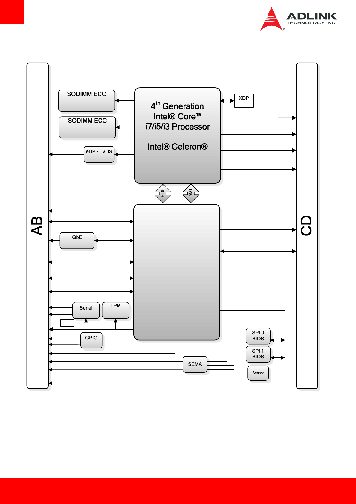
2.15 Function Diagram
1333/1600 MHz
1~8 GB DDR3L
1333/1600 MHz
1~8 GB DDR3L
single / dual
18/24-bit LVDS
2x SATA3 & 2x SATA2 (HM86)
RTD2136R
VGA
6x PCIe x1 (Gen2)
(port 0~5)
i217LM
4x SATA3 (QM87)
8x USB 1.1/2.0
HD Audio
PCIe x1
(port 7)
eDP
2 lane
“Haswell”
Mobile Intel®
QM87/HM86
Chipset
60-pin
(
p
o
r
t
)
B
I
D
D
1
I / D
M
D
/ H
P
D
DDI 2 (port C)
DP / HDMI / DVI
DDI 3 (port D)
DP / HDMI / DVI
PCI Express x16 (Gen3)
2 x8 or 1 x8 + 2 x4
4x USB 3.0 upgrade (QM87)
2x USB 3.0 upgrade (HM86)
1x PCIe x1 (Gen2)
(port 6)
O
V
D
/ S
I
V
UART0
UART1
4x GP0
4x GPI
Debug
header
SMBus
NCT5104D
LPC bus
PCA9535
GP I2C
DDC I2C
ATMEL
AT97SC3204
SPI_CS#
SPI
SPI_CS0
SPI_CS1
-40+85°C
Page 10 Express-HLE
Page 11
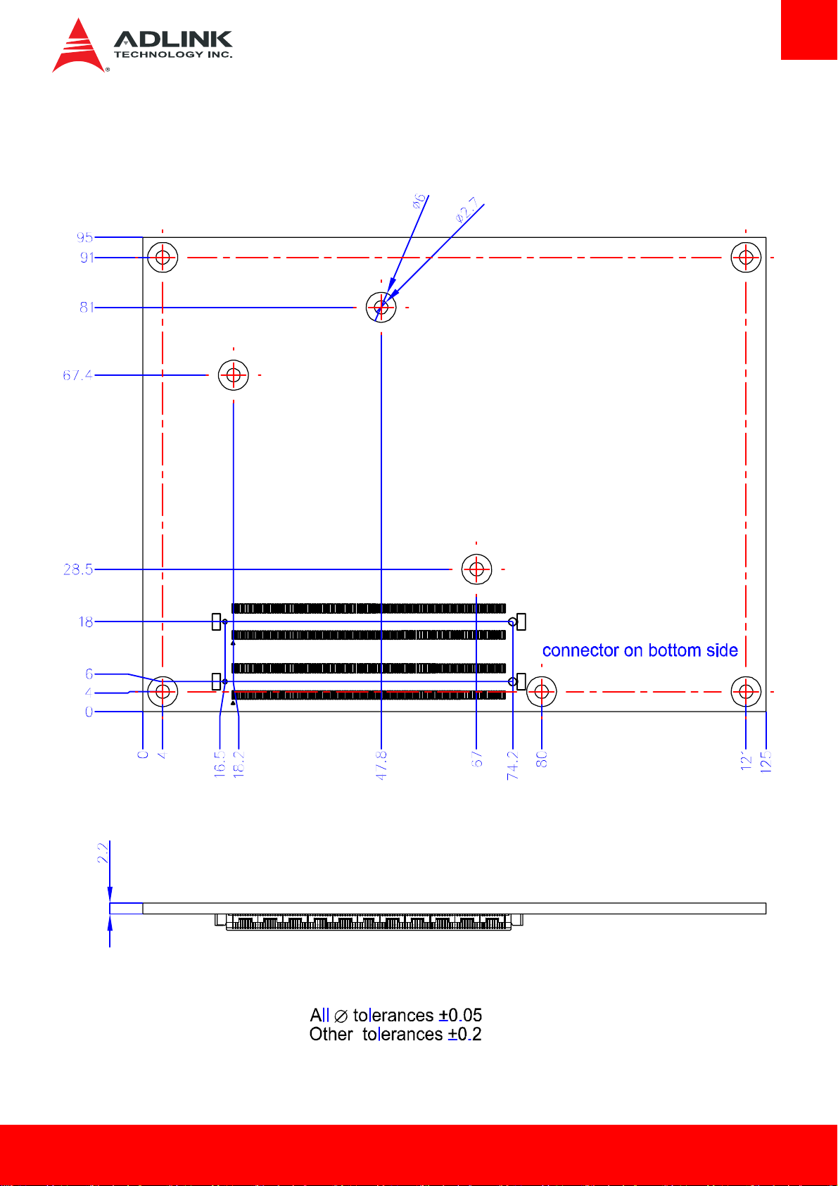
2.16 Mechanical Drawing
Express-HLE Page 11
Page 12
3 Pinouts and Signal Descriptions
3.1 AB / CD Pin Definitions
The Express-HLE is a Type 6 module supporting USB3.0 and DDI channels on the CD connector
All pins in the COM Express specification are described, including those not supported on the Express-HLE. Those not supported on the
Express-HLE module are crossed out
Row A Row B Row C Row D
Pin Name Pin Name Pin Name Pin Name
A1
A2
A3
A4
A5
A6
A7
A8
A9
A10
A11
A12
A13
A14
A15
A16
A17
A18
A19
A20
A21
A22
A23
A24
A25
A26
A27
A28
A29
A30
A31
A32
A33
A34
A35
GND (FIXED)
GBE0_MDI3GBE0_MDI3+
GBE0_LINK100#
GBE0_LINK1000#
GBE0_MDI2GBE0_MDI2+
GBE0_LINK#
GBE0_MDI1GBE0_MDI1+
GND (FIXED)
GBE0_MDI0GBE0_MDI0+
GBE0_CTREF
SUS_S3#
SATA0_TX+
SATA0_TX-
SUS_S4#
SATA0_RX+
SATA0_RXGND (FIXED)
SATA2_TX+
SATA2_TX-
SUS_S5#
SATA2_RX+
SATA2_RX-
BATLOW#
(S)ATA_ACT#
AC/HDA_SYNC
AC/HDA_RST#
GND (FIXED)
AC/HDA_BITCLK
AC/HDA_SDOUT
BIOS_DIS0#
THRMTRIP#
B1
B2
B3
B4
B5
B6
B7
B8
B9
B10
B11
B12
B13
B14
B15
B16
B17
B18
B19
B20
B21
B22
B23
B24
B25
B26
B27
B28
B29
B30
B31
B32
B33
B34
B35
GND (FIXED)
GBE0_ACT#
LPC_FRAME#
LPC_AD0
LPC_AD1
LPC_AD2
LPC_AD3
LPC_DRQ0#
LPC_DRQ1#
LPC_CLK
GND (FIXED)
PWRBTN#
SMB_CK
SMB_DAT
SMB_ALERT#
SATA1_TX+
SATA1_TX-
SUS_STAT#
SATA1_RX+
SATA1_RXGND (FIXED)
SATA3_TX+
SATA3_TX-
PWR_OK
SATA3_RX+
SATA3_RX-
WDT
AC/HDA_SDIN2
AC/HDA_SDIN1
AC/HDA_SDIN0
GND (FIXED)
SPKR
I2C_CK
I2C_DAT
THRM#
C1
C2
C3
C4
C5
C6
C7
C8
C9
C10
C11
C12
C13
C14
C15
C16
C17
C18
C19
C20
C21
C22
C23
C24
C25
C26
C27
C28
C29
C30
C31
C32
C33
C34
C35
GND FIXED)
GND
USB_SSRX0USB_SSRX0+
GND
USB_SSRX1USB_SSRX1+
GND
USB_SSRX2- *
USB_SSRX2+ *
GND (FIXED)
USB_SSRX3- *
USB_SSRX3+ *
GND
DDI1_PAIR6+
DDI1_PAIR6RSVD
RSVD
PCIE_RX6+
PCIE_RX6GND (FIXED)
PCIE_RX7+
PCIE_RX7DDI1_HPD
DDI1_PAIR4+
DDI1_PAIR4RSVD
RSVD
DDI1_PAIR5+
DDI1_PAIR5GND (FIXED)
DDI2_CTRLCLK_AUX+
DDI2_CTRLDATA_AUXDDI2_DDC_AUX_SEL
RSVD
D1
D2
D3
D4
D5
D6
D7
D8
D9
D10
D11
D12
D13
D14
D15
D16
D17
D18
D19
D20
D21
D22
D23
D24
D25
D26
D27
D28
D29
D30
D31
D32
D33
D34
D35
GND FIXED)
GND
USB_SSTX0USB_SSTX0+
GND
USB_SSTX1USB_SSTX1+
GND
USB_SSTX2- *
USB_SSTX2+ *
GND (FIXED)
USB_SSTX3- *
USB_SSTX3+ *
GND
DDI1_CTRLCLK_AUX+
DDI1_CTRLDATA_AUX
RSVD
RSVD
PCIE_TX6+
PCIE_TX6GND (FIXED)
PCIE_TX7+
PCIE_TX7RSVD
RSVD
DDI1_PAIR0+
DDI1_PAIR0RSVD
DDI1_PAIR1+
DDI1_PAIR1GND (FIXED)
DDI1_PAIR2+
DDI1_PAIR2-
DDI1_DDC_AUX_SEL
RSVD
Page 12 Express-HLE
Page 13
Row A Row B Row C Row D
Pin Name Pin Name Pin Name Pin Name
A36
A37
A38
A39
A40
A41
A42
A43
A44
A45
A46
A47
A48
A49
A50
A51
A52
A53
A54
A55
A56
A57
A58
A59
A60
A61
A62
A63
A64
A65
A66
A67
A68
A69
A70
A71
A72
A73
A74
A75
A76
A77
A78
A79
A80
USB6USB6+
USB_6_7_OC#
USB4USB4+
GND (FIXED)
USB2USB2+
USB_2_3_OC#
USB0USB0+
VCC_RTC
EXCD0_PERST#
EXCD0_CPPE#
LPC_SERIRQ
GND (FIXED)
PCIE_TX5+
PCIE_TX5-
GPI0
PCIE_TX4+
PCIE_TX4GND
PCIE_TX3+
PCIE_TX3GND (FIXED)
PCIE_TX2+
PCIE_TX2GPI1
PCIE_TX1+
PCIE_TX1GND
GPI2
PCIE_TX0+
PCIE_TX0GND (FIXED)
LVDS_A0+
LVDS_A0LVDS_A1+
LVDS_A1LVDS_A2+
LVDS_A2LVDS_VDD_EN
LVDS_A3+
LVDS_A3GND (FIXED)
B36
B37
B38
B39
B40
B41
B42
B43
B44
B45
B46
B47
B48
B49
B50
B51
B52
B53
B54
B55
B56
B57
B58
B59
B60
B61
B62
B63
B64
B65
B66
B67
B68
B69
B70
B71
B72
B73
B74
B75
B76
B77
B78
B79
B80
USB7USB7+
USB_4_5_OC#
USB5USB5+
GND (FIXED)
USB3USB3+
USB_0_1_OC#
USB1USB1+
EXCD1_PERST#
EXCD1_CPPE#
SYS_RESET#
CB_RESET#
GND (FIXED)
PCIE_RX5+
PCIE_RX5-
GPO1
PCIE_RX4+
PCIE_RX4GPO2
PCIE_RX3+
PCIE_RX3GND (FIXED)
PCIE_RX2+
PCIE_RX2GPO3
PCIE_RX1+
PCIE_RX1-
WAKE0#
WAKE1#
PCIE_RX0+
PCIE_RX0GND (FIXED)
LVDS_B0+
LVDS_B0LVDS_B1+
LVDS_B1LVDS_B2+
LVDS_B2LVDS_B3+
LVDS_B3LVDS_BKLT_EN
GND (FIXED)
C36
C37
C38
C39
C40
C41
C42
C43
C44
C45
C46
C47
C48
C49
C50
C51
C52
C53
C54
C55
C56
C57
C58
C59
C60
C61
C62
C63
C64
C65
C66
C67
C68
C69
C70
C71
C72
C73
C74
C75
C76
C77
C78
C79
C80
DDI3_CTRLCLK_AUX+
DDI3_CTRLDATA_AUXDDI3_DDC_AUX_SEL
DDI3_PAIR0+
DDI3_PAIR0GND (FIXED)
DDI3_PAIR1+
DDI3_PAIR1DDI3_HPD
RSVD
DDI3_PAIR2+
DDI3_PAIR2RSVD
DDI3_PAIR3+
DDI3_PAIR3GND (FIXED)
PEG_RX0+
PEG_RX0-
TYPE0#
PEG_RX1+
PEG_RX1-
TYPE1#
PEG_RX2+
PEG_RX2GND (FIXED)
PEG_RX3+
PEG_RX3RSVD
RSVD
PEG_RX4+
PEG_RX4RSVD
PEG_RX5+
PEG_RX5GND (FIXED)
PEG_RX6+
PEG_RX6GND
PEG_RX7+
PEG_RX7GND
RSVD
PEG_RX8+
PEG_RX8GND (FIXED)
D36
D37
D38
D39
D40
D41
D42
D43
D44
D45
D46
D47
D48
D49
D50
D51
D52
D53
D54
D55
D56
D57
D58
D59
D60
D61
D62
D63
D64
D65
D66
D67
D68
D69
D70
D71
D72
D73
D74
D75
D76
D77
D78
D79
D80
DDI1_PAIR3+
DDI1_PAIR3RSVD
DDI2_PAIR0+
DDI2_PAIR0GND (FIXED)
DDI2_PAIR1+
DDI2_PAIR1DDI2_HPD
RSVD
DDI2_PAIR2+
DDI2_PAIR2RSVD
DDI2_PAIR3+
DDI2_PAIR3GND (FIXED)
PEG_TX0+
PEG_TX0-
PEG_LANE_RV#
PEG_TX1+
PEG_TX1-
TYPE2#
PEG_TX2+
PEG_TX2GND (FIXED)
PEG_TX3+
PEG_TX3RSVD
RSVD
PEG_TX4+
PEG_TX4GND
PEG_TX5+
PEG_TX5GND (FIXED)
PEG_TX6+
PEG_TX6GND
PEG_TX7+
PEG_TX7GND
RSVD
PEG_TX8+
PEG_TX8GND (FIXED)
Express-HLE Page 13
Page 14
Row A Row B Row C Row D
Pin Name Pin Name Pin Name Pin Name
A81
A82
A83
A84
A85
A86
A87
A88
A89
A90
A91
A92
A93
A94
A95
A96
A97
A98
A99
A100
A101
A102
A103
A104
A105
A106
A107
A108
A109
A110
LVDS_A_CK+
LVDS_A_CKLVDS_I2C_CK
LVDS_I2C_DAT
GPI3
RSVD
RSVD
PCIE0_CK_REF+
PCIE0_CK_REF-
GND (FIXED)
SPI_POWER
SPI_MISO
GPO0
SPI_CLK
SPI_MOSI
TPM_PP
TYPE10#
SER0_TX
SER0_RX
GND (FIXED)
SER1_TX
SER1_RX
LID#
VCC_12V
VCC_12V
VCC_12V
VCC_12V
VCC_12V
VCC_12V
GND (FIXED)
B81
B82
B83
B84
B85
B86
B87
B88
B89
B90
B91
B92
B93
B94
B95
B96
B97
B98
B99
B100
B101
B102
B103
B104
B105
B106
B107
B108
B109
B110
LVDS_B_CK+
LVDS_B_CKLVDS_BKLT_CTRL
VCC_5V_SBY
VCC_5V_SBY
VCC_5V_SBY
VCC_5V_SBY
BIOS_DIS1#
VGA_RED
GND (FIXED)
VGA_GRN
VGA_BLU
VGA_HSYNC
VGA_VSYNC
VGA_I2C_CK
VGA_I2C_DAT
SPI_CS#
RSVD
RSVD
GND (FIXED)
FAN_PWMOUT
FAN_TACHIN
SLEEP#
VCC_12V
VCC_12V
VCC_12V
VCC_12V
VCC_12V
VCC_12V
GND (FIXED)
C81
C82
C83
C84
C85
C86
C87
C88
C89
C90
C91
C92
C93
C94
C95
C96
C97
C98
C99
C100
C101
C102
C103
C104
C105
C106
C107
C108
C109
C110
PEG_RX9+
PEG_RX9-
TPM_PP
GND
PEG_RX10+
PEG_RX10GND
PEG_RX11+
PEG_RX11GND (FIXED)
PEG_RX12+
PEG_RX12GND
PEG_RX13+
PEG_RX13GND
RSVD
PEG_RX14+
PEG_RX14GND (FIXED)
PEG_RX15+
PEG_RX15GND
VCC_12V
VCC_12V
VCC_12V
VCC_12V
VCC_12V
VCC_12V
GND (FIXED)
D81
D82
D83
D84
D85
D86
D87
D88
D89
D90
D91
D92
D93
D94
D95
D96
D97
D98
D99
D100
D101
D102
D103
D104
D105
D106
D107
D108
D109
D110
PEG_TX9+
PEG_TX9RSVD
GND
PEG_TX10+
PEG_TX10GND
PEG_TX11+
PEG_TX11GND (FIXED)
PEG_TX12+
PEG_TX12GND
PEG_TX13+
PEG_TX13GND
RSVD
PEG_TX14+
PEG_TX14GND (FIXED)
PEG_TX15+
PEG_TX15GND
VCC_12V
VCC_12V
VCC_12V
VCC_12V
VCC_12V
VCC_12V
GND (FIXED)
*Note: USB 3.0 upgrade signals for ports 2, 3 are supported by QM87 only.
Page 14 Express-HLE
Page 15

3.2 Signal Description Terminology
The following terms are used in the COM Express AB/CD Signal Descriptions below.
I Input to the Module
O Output from the Module
I/O Bi-directional input / output signal
OD Open drain output
I 3.3V Input 3.3V tolerant
I 5V Input 5V tolerant
O 3.3V Output 3.3V signal level
O 5V Output 5V signal level
I/O 3.3V Bi-directional signal 3.3V tolerant
I/O 5V Bi-directional signal 5V tolerant
I/O 3.3Vsb Input 3.3V tolerant active in standby state
P Power Input/Output
REF Reference voltage output that may be sourced from a module power plane.
PDS Pull-down strap. This is an output pin on the module that is either tied to GND or not connected.
The signal is used to indicate the PICMG module type to the Carrier Board.
PU ADLINK implemented pull-up resistor on module
PD ADLINK implemented pull-down resistor on module
Express-HLE Page 15
Page 16
3.3 AB Signal Descriptions
3.3.1 Audio Signals
Signal Pin # Description I/O PU/PD Comment
AC_RST# /
HDA_RST#
AC_SYNC /
HDA_SYNC
AC_BITCLK /
HDA_BITCLK
AC _SDOUT /
HDA_SDOUT
AC _SDIN[2:0]
HDA_SDIN[2:0]
A30 Reset output to codec, active low. O 3.3VSB VSB because PCH uses suspend
power for RESET
A29 Sample-synchronization signal to the codec(s). O 3.3V
A32 Serial data clock generated by the external
codec(s).
A33 Serial TDM data output to the codec. O 3.3V
B28
B30
Serial TDM data inputs from up to 3 codecs. I/O 3.3V
I/O 3.3V
3.3.2 Analog VGA
Signal Pin # Description I/O PU/PD Comment
VGA_RED B89 Red for monitor.
Analog DAC output, designed to drive a
37.5-Ohm equivalent load.
VGA_GRN B91 Green for monitor
Analog DAC output, designed to drive a
37.5-Ohm equivalent load.
O Analog
O Analog
PD 150R
PD 150R
Shall also be terminated on the
carrier with 150Ω resistor to
ground close to VGA connector
Shall also be terminated on the
carrier with 150Ω resistor to
ground close to VGA connector
VGA_BLU B92 Blue for monitor.
Analog DAC output, designed to drive a
37.5-Ohm equivalent load.
VGA_HSYNC B93 Horizontal sync output to VGA monitor O 3.3V
VGA_VSYNC B94 Vertical sync output to VGA monitor O 3.3V
VGA_I2C_CK B95 DDC clock line (I²C port dedicated to identify
VGA monitor capabilities)
VGA_I2C_DAT B96 DDC data line. I/O OD 3.3V PU 2k2 3.3V
O Analog
I/O OD 3.3V PU 2k2 3.3V
PD 150R
Shall also be terminated on the
carrier with 150Ω resistor to
ground close to VGA connector
Page 16 Express-HLE
Page 17
3.3.3 LVDS
Signal Pin # Description I/O PU/PD Comment
LVDS_A0+
LVDS_A0-
LVDS_A1+
LVDS_A1-
LVDS_A2+
LVDS_A2-
LVDS_A3+
LVDS_A3-
LVDS_A_CK+
LVDS_A_CK-
LVDS_B0+
LVDS_B0-
LVDS_B1+
LVDS_B1-
LVDS_B2+
LVDS_B2-
LVDS_B3+
LVDS_B3-
LVDS_B_CK+
LVDS_B_CK-
LVDS_VDD_EN A77 LVDS panel power enable O 3.3V
LVDS_BKLT_EN B79 LVDS panel backlight enable O 3.3V
LVDS_BKLT_CTRL B83 LVDS panel backlight brightness control O 3.3V PD 100K
A71
A72
A73
A74
A75
A76
A78
A79
A81
A82
B71
B72
B73
B74
B75
B76
B77
B78
B81
B82
LVDS Channel A differential pairs O LVDS
LVDS Channel A differential clock O LVDS
LVDS Channel B differential pairs O LVDS
LVDS Channel B differential clock O LVDS
Realtek ePD to LVDS
requirement
LVDS_I2C_CK A83 DDC lines used for flat panel detection and control. O 3.3V PU 2k2 3.3V
LVDS_I2C_DAT A84 DDC lines used for flat panel detection and control. I/O 3.3V PU 2k2 3.3V
3.3.4 Gigabit Ethernet
Gigabit Ethernet Pin # Description I/O PU/PD Comment
GBE0_MDI0+
GBE0_MDI0-
GBE0_MDI1+
GBE0_MDI1-
GBE0_MDI2+
GBE0_MDI2-
GBE0_MDI3+
GBE0_MDI3-
GBE0_ACT# B2 Gigabit Ethernet Controller 0 activity indicator, active low. O 3.3VSB PU 10k
GBE0_LINK# A8 Gigabit Ethernet Controller 0 link indicator, active low. O 3.3VSB
GBE0_LINK100# A4 Gigabit Ethernet Controller 0 100Mbit/sec link indicator, active low. O 3.3VSB
GBE0_LINK1000# A5 Gigabit Ethernet Controller 0 1000Mbit/sec link indicator, active low. O 3.3VSB
GBE0_CTREF A14 Reference voltage for Carrier Board Ethernet channel 1 and 2 magnetics
A13
A12
A10
A9
A7
A6
A3
A2
Gigabit Ethernet Controller 0: Media Dependent Interface Differential Pairs
0, 1, 2, 3. The MDI can operate in 1000, 100, and 10Mbit/sec modes.
Some pairs are unused in some modes according to the following:
1000BASE-T 100BASE-TX 10BASE-T
MDI[0]+/- B1_DA+/- TX+/- TX+/-
MDI[1]+/- B1_DB+/- RX+/- RX+/-
MDI[2]+/- B1_DC+/MDI[3]+/- B1_DD+/-
center tap. The reference voltage is determined by the requirements of the
Module PHY and may be as low as 0V and as high as 3.3V. The reference
voltage output shall be current limited on the Module. In the case in which
the reference is shorted to ground, the current shall be 250 mA or less.
I/O Analog Twisted pair
signals for
external
transformer.
3.3VSB
GND min
3.3V max
Express-HLE Page 17
Page 18
3.3.5 Serial ATA
Signal Pin # Description I/O PU/PD Comment
SATA0_TX+
SATA0_TX-
SATA0_RX+
SATA0_RX-
SATA1_TX+
SATA1_TX-
SATA1_RX+
SATA1_RX-
SATA2_TX+
SATA2_TX-
SATA2_RX+
SATA2_RX-
SATA3_TX+
SATA3_TX-
SATA3_RX+
SATA3_RX-
(S)ATA_ACT# A28 ATA (parallel and serial) or SAS activity
A16
Serial ATA channel 0, Transmit Output
A17
differential pair.
A19
Serial ATA channel 0, Receive Input
A20
differential pair.
B16
Serial ATA channel 1, Transmit Output
B17
differential pair.
B19
Serial ATA channel 1, Receive Input
B20
differential pair.
A22
Serial ATA channel 2, Transmit Output
A23
differential pair.
A25
Serial ATA channel 2, Receive Input
A26
differential pair.
B22
Serial ATA channel 3, Transmit Output
B23
differential pair.
B25
Serial ATA channel 3, Receive Input
B26
differential pair.
indicator, active low.
O SATA AC coupled on Module
I SATA AC coupled on Module
O SATA AC coupled on Module
I SATA AC coupled on Module
O SATA AC coupled on Module
I SATA AC coupled on Module
O SATA AC coupled on Module
I SATA AC coupled on Module
O 3.3V
Page 18 Express-HLE
Page 19
3.3.6 PCI Express
Signal Pin # Description I/O PU/PD Comment
PCIE_TX0+
PCIE_TX0-
PCIE_RX0+
PCIE_RX0-
PCIE_TX1+
PCIE_TX1-
PCIE_RX1+
PCIE_RX1-
PCIE_TX2+
PCIE_TX2-
PCIE_RX2+
PCIE_RX2-
PCIE_TX3+
PCIE_TX3-
PCIE_RX3+
PCIE_RX3-
PCIE_TX4+
PCIE_TX4-
PCIE_RX4+
PCIE_RX4-
PCIE_TX5+
PCIE_TX5-
A68
A69
B68
B69
A64
A65
B64
B65
A61
A62
B61
B62
A58
A59
B58
B59
A55
A56
B55
B56
A52
A53
PCI Express channel 0, Transmit Output differential
pair.
PCI Express channel 0, Receive Input differential
pair.
PCI Express channel 1, Transmit Output differential
pair.
PCI Express channel 1, Receive Input differential
pair.
PCI Express channel 2, Transmit Output differential
pair.
PCI Express channel 2, Receive Input differential
pair.
PCI Express channel 3, Transmit Output differential
pair.
PCI Express channel 3, Receive Input differential
pair.
PCI Express channel 4, Transmit Output differential
pair.
PCI Express channel 4, Receive Input differential
pair.
PCI Express channel 5, Transmit Output differential
pair.
O PCIE AC coupled on Module
I PCIE AC coupled off Module
O PCIE AC coupled on Module
I PCIE AC coupled off Module
O PCIE AC coupled on Module
I PCIE AC coupled off Module
O PCIE AC coupled on Module
I PCIE AC coupled off Module
O PCIE AC coupled on Module
I PCIE AC coupled off Module
O PCIE AC coupled on Module
PCIE_RX5+
PCIE_RX5-
PCIE_CLK_REF+
PCIE_CLK_REF-
B52
B53
A88
A89
PCI Express channel 5, Receive Input differential
pair.
PCI Express Reference Clock output for all PCI
Express and PCI Express Graphics Lanes.
I PCIE AC coupled off Module
O PCIE
3.3.7 Express Card
Signal Pin # Description I/O PU/PD Comment
EXCD0_CPPE#
EXCD1_CPPE#
EXCD0_PERST#
EXCD1_PERST#
A49
B48
A48
B47
PCI ExpressCard: PCI Express capable card request I 3.3V PU 10k 3.3V
PCI ExpressCard: reset O 3.3V
3.3.8 LPC Bus
Signal Pin # Description I/O PU/PD Comment
LPC_AD[0:3] B4-B7 LPC multiplexed address, command and data bus I/O 3.3V
LPC_FRAME# B3 LPC frame indicates the start of an LPC cycle O 3.3V
LPC_DRQ0#
LPC_DRQ1#
B8
B9
LPC serial DMA request I 3.3V
LPC_SERIRQ A50 LPC serial interrupt I/O OD 3.3V PU 8k2 3.3V
LPC_CLK B10 LPC clock output - 33MHz nominal O 3.3V
Express-HLE Page 19
Page 20

3.3.9 USB
Signal Pin # Description I/O PU/PD Comment
USB0+
USB0-
USB1+
USB1-
USB2+
USB2-
USB3+
USB3-
USB4+
USB4-
USB5+
USB5-
USB6+
USB6-
USB7+
USB7-
USB_0_1_OC# B44 USB over-current sense, USB ports 0 and 1. A pull-up
A46
USB differential data pairs for Port 0 I/O 3.3VSB USB 1.1/ 2.0 compliant
A45
B46
USB differential data pairs for Port 1 I/O 3.3VSB USB 1.1/ 2.0 compliant
B45
A43
USB differential data pairs for Port 1 I/O 3.3VSB USB 1.1/ 2.0 compliant
A42
B43
USB differential data pairs for Port 2 I/O 3.3VSB USB 1.1/ 2.0 compliant
B42
A40
USB differential data pairs for Port 3 I/O 3.3VSB USB 1.1/ 2.0 compliant
A39
B40
USB differential data pairs for Port 4 I/O 3.3VSB USB 1.1/ 2.0 compliant
B39
A37
USB differential data pairs for Port 5 I/O 3.3VSB USB 1.1/ 2.0 compliant
A36
B37
USB differential data pairs for Port 6 I/O 3.3VSB USB 1.1/ 2.0 compliant
B37
for this line shall be present on the module. An open
drain driver from a USB current monitor on the carrier
board may drive this line low.
I 3.3VSB PU 10k 3.3VSB Do not pull high on carrier
USB_2_3_OC# A44 USB over-current sense, USB ports 2 and 3. A pull-up
for this line shall be present on the module. An open
drain driver from a USB current monitor on the carrier
board may drive this line low. .
USB_4_5_OC# B38 USB over-current sense, USB ports 4 and 5. A pull-up
for this line shall be present on the module. An open
drain driver from a USB current monitor on the carrier
board may drive this line low.
USB_6_7_OC# A38 USB over-current sense, USB ports 6 and 7. A pull-up
for this line shall be present on the module. An open
drain driver from a USB current monitor on the carrier
board may drive this line low.
I 3.3VSB PU 10k 3.3VSB Do not pull high on carrier
I 3.3VSB PU 10k 3.3VSB Do not pull high on carrier
I 3.3VSB PU 10k 3.3VSB Do not pull high on carrier
Page 20 Express-HLE
Page 21
3.3.10 USB Root Segmentation
Express-HLE Page 21
Page 22
3.3.11 SPI (BIOS only)
Signal Pin # Description I/O PU/PD Comment
SPI_CS# B97 Chip select for Carrier Board SPI BIOS Flash. O 3.3VSB
SPI_MISO A92 Data in to module from carrier board SPI BIOS flash. I 3.3VSB
SPI_MOSI A95 Data out from module to carrier board SPI BIOS flash. O 3.3VSB
SPI_CLK A94 Clock from module to carrier board SPI BIOS flash. O 3.3VSB
SPI_POWER A91 Power supply for Carrier Board SPI – sourced from Module
– nominally 3.3V.
The Module shall provide a minimum of 100mA on
SPI_POWER.
Carriers shall use less than 100mA of SPI_POWER.
SPI_POWER shall only be used to power SPI devices on
the Carrier
BIOS_DIS0# A34 Selection strap to determine the BIOS boot device. I PU 10K 3.3V Carrier shall pull to GND
BIOS_DIS1# B88 Selection strap to determine the BIOS boot device. I PU 10K 3.3V Carrier shall pull to GND
O P 3.3VSB
or leave no- connect.
or leave no- connect
3.3.12 Miscellaneous
Signal Pin # Description I/O PU/PD Comment
SPKR B32 Output for audio enunciator, the “speaker” in PC-AT
systems
WDT B27 Output indicating that a watchdog time-out event has
occurred.
THRM# B35 Input from off-module temp sensor indicating an over-temp
situation.
THERMTRIP# A35 Active low output indicating that the CPU has entered
thermal shutdown.
O 3.3V
O 3.3V
I 3.3V
O 3.3V PU 330 3.3V
FAN_PWMOUT B101 Fan speed control. Uses the Pulse Width Modulation
(PWM) technique to control the fan’s RPM.
FAN_TACHIN11 B102 Fan tachometer input for a fan with a two pulse output. I OD 3.3V PU 10k 3.3V
TPM_PP11 C83 Trusted Platform Module (TPM) Physical Presence pin.
Active high. TPM chip has an internal pull down. This
signal is used to indicate Physical Presence to the TPM.
O OD 3.3V
I 3.3V
PD 10k 3.3V
PD is only placed
when TPM is
installed on module
3.3.13 SMBus
Signal Pin # Description I/O PU/PD Comment
SMB_CK B13 System Management Bus bidirectional clock line. Power
sourced through 5V standby rail and main power rails.
SMB_DAT# B14 System Management Bus bidirectional data line. Power
sourced through 5V standby rail and main power rails.
SMB_ALERT# B15 System Management Bus Alert – active low input can
be used to generate an SMI# (System Management
Interrupt) or to wake the system. Power sourced
through 5V standby rail and main power rails.
Page 22 Express-HLE
I/O OD 3.3VSB PU 2k2 3.3VSB
I/O OD 3.3VSB PU 2k2 3.3VSB
I 3.3VSB PU 10k 3.3VSB
Page 23
3.3.14 I2C Bus
Signal Pin # Description I/O PU/PD Comment
I2C_CK B33 General purpose I²C port clock output/input I/O OD 3.3VSB PU 2k2 3.3VSB
I2C_DAT B34 General purpose I²C port data I/O line I/O OD 3.3VSB PU 2k2 3.3VSB
3.3.15 General Purpose I/O (GPIO)
Signal Pin # Description I/O PU/PD Comment
GPO[0] A93 General purpose output pins. O 3.3V After hardware RESET
output low
GPO[1] B54 General purpose output pins. O 3.3V After hardware RESET
output low
GPO[2] B57 General purpose output pins. O 3.3V After hardware RESET
output low
GPO[3] B63 General purpose output pins. O 3.3V After hardware RESET
output low
GPI[0] A54 General purpose input pins.
Pulled high internally on the module.
GPI[1] A63 General purpose input pins.
Pulled high internally on the module.
GPI[2] A67 General purpose input pins.
Pulled high internally on the module.
GPI[3] A85 General purpose input pins.
Pulled high internally on the module.
I 3.3V PU 10K 3.3V
I 3.3V PU 10K 3.3V
I 3.3V PU 10K 3.3V
I 3.3V PU 10K 3.3V
3.3.16 Serial Interface Signals
Signal Pin # Description I/O PU/PD Comment
SER0_TX A98 General purpose serial port transmitter (TTL level output) O CMOS Power rail tolerance 5V / 12V
SER0_RX A99 General purpose serial port receiver (TTL level input) I CMOS Power rail tolerance 5V / 12V
SER1_TX A101 General purpose serial port transmitter (TTL level output) O CMOS Power rail tolerance 5V / 12V
SER1_RX A102 General purpose serial port receiver (TTL level input) I CMOS Power rail tolerance 5V / 12V
Express-HLE Page 23
Page 24
3.3.17 Power And System Management
Signal Pin # Description I/O PU/PD Comment
PWRBTN# B12 Power button to bring system out of S5 (soft off), active on falling edge. I 3.3VSB PU 10k
3.3VSB
SYS_RESET# B49 Reset button input. Active low request for module to reset and reboot. May
be falling edge sensitive. For situations when SYS_RESET# is not able to
reestablish control of the system, PWR_OK or a power cycle may be used.
CB_RESET# B50 Reset output from module to Carrier Board. Active low. Issued by module
chipset and may result from a low SYS_RESET# input, a low PWR_OK
input, a VCC_12V power input that falls below the minimum specification, a
watchdog timeout, or may be initiated by the module software.
PWR_OK B24 Power OK from main power supply. A high value indicates that the power is
good. This signal can be used to hold off Module startup to allow carrier
based FPGAs or other configurable devices time to be programmed.
SUS_STAT# B18 Indicates imminent suspend operation; used to notify LPC devices. O 3.3VSB
SUS_S3# A15 Indicates system is in Suspend to RAM state. Active-low output. An inverted
copy of SUS_S3# on the carrier board (also known as “PS_ON”) may be
used to enable the non-standby power on a typical ATX power supply.
SUS_S4# A18 Indicates system is in Suspend to Disk state. Active low output. O 3.3VSB
SUS_S5# A24 Indicates system is in Soft Off state. O 3.3VSB
WAKE0# B66 PCI Express wake up signal. I 3.3VSB PU 10k
WAKE1# B67 General purpose wake up signal. May be used to implement wake-up on
PS/2 keyboard or mouse activity.
I 3.3VSB PU 10k
3.3VSB
O 3.3VSB
I 3.3V PU 100k
3.3VSB
O 3.3VSB
3.3VSB
I 3.3VSB PU 10k
3.3VSB
Should have
weak pull up
BATLOW# A27 Battery low input. This signal may be driven low by external circuitry to
signal that the system battery is low, or may be used to signal some other
external power-management event.
LID# LID button. Low active signal used by the ACPI operating system for a LID
switch.
SLEEP# Sleep button. Low active signal used by the ACPI operating system to bring
the system to sleep state or to wake it up again.
I 3.3VSB PU 10k
3.3VSB
I OD
3.3VSB
I OD
3.3VSB
PU 10k
3.3VSB
PU 10K
3.3VSB
3.3.18 Power and Ground
Signal Pin # Description I/O PU/PD Comment
VCC_12V A104-A109
B104-B109
VCC_5V_SBY B84-B87 Standby power input: +5.0V nominal. If VCC5_SBY is used, all
VCC_RTC A47 Real-time clock circuit-power input. Nominally +3.0V. P
GND A1, A11, A21, A31,
A41, A51, A57, A66,
A80, A90, A96,
A100, A110, B1,
B11, B21 ,B31, B41,
B51, B60, B70, B80,
B90, B100, B110
Primary power input: +12V nominal (8.5 ~ 20V wide input).
All available VCC_12V pins on the connector(s) shall be used.
available VCC_5V_SBY pins on the connector(s) shall be used.
Only used for standby and suspend functions. May be left
unconnected if these functions are not used in the system design.
Ground - DC power and signal and AC signal return path. P
P 8.5~20 V
P 5Vsb ±5%
Page 24 Express-HLE
Page 25
3.4 CD Signal Descriptions
3.4.1 USB 3.0 extension
Signal Pin Description I/O PU/PD Comment
USB_SSRX0-
USB_SSRX0+
USB_SSTX0-
USB_SSTX0+
USB_SSRX1-
USB_SSRX1+
USB_SSTX1-
USB_SSTX1+
USB_SSRX2-
USB_SSRX2+
USB_SSTX2-
USB_SSTX2+
USB_SSRX3-
USB_SSRX3+
USB_SSTX3-
USB_SSTX3+
C3
C4
D3
D4
C6
C7
D6
D7
C9
C10
D9
D10
C12
C13
D12
D13
Additional Receive signal differential pairs for the
SuperSpeed USB data path on USB0
Additional Transmit signal differential pairs for the
SuperSpeed USB data path on USB0
Additional Receive signal differential pairs for the
SuperSpeed USB data path on USB1
Additional Transmit signal differential pairs for the
SuperSpeed USB data path on USB1
Additional Receive signal differential pairs for the
SuperSpeed USB data path on USB2
Additional Transmit signal differential pairs for the
SuperSpeed USB data path on USB2
Additional Receive signal differential pairs for the
SuperSpeed USB data path on USB3
Additional Transmit signal differential pairs for the
SuperSpeed USB data path on USB3
I PCIE
O PCIE AC coupled on Module
I PCIE
O PCIE AC coupled on Module
I PCIE
O PCIE AC coupled on Module
I PCIE
O PCIE AC coupled on Module
3.4.2 PCI Express x1
Signal Pin # Description I/O PU/PD Comment
PCIE_TX6+
PCIE_TX6-
PCIE_RX6+
PCIE_RX6-
PCIE_TX7+
PCIE_TX7-
PCIE_RX7+
PCIE_RX7-
D19
D20
C19
C20
D22
D23
C22
C23
PCI Express channel 6, Transmit Output
differential pair.
PCI Express channel 6, Receive Input
differential pair.
PCI Express channel 7, Transmit Output
differential pair.
PCI Express channel 7, Receive Input
differential pair.
O PCIE AC coupled on Module
I PCIE AC coupled off Module
O PCIE Not available used by LAN
I PCIE Not available used by LAN
Express-HLE Page 25
Page 26
3.4.3 DDI Channels
DDI 1
Signal Pin Description I/O PU/PD Comment
DDI1_PAIR0+
DDI1_PAIR0DDI1_PAIR1+
DDI1_PAIR1DDI1_PAIR2+
DDI1_PAIR2DDI1_PAIR3+
DDI1_PAIR3DDI1_PAIR4+
DDI1_PAIR4DDI1_PAIR5+
DDI1_PAIR5DDI1_PAIR6+
DDI1_PAIR6-
DDI1_HPD C24 Digital Display Interface Hot-Plug Detect I PCIE
DDI1_DDC_AUX_SEL D34 Selects the function of DDI1_CTRLCLK_AUX+
D26
D27
D29
D30
D32
D33
D36
D37
C25
C26
C29
C30
C15
C16
Digital Display Interface1 differential pairs O PCIE
IF DDI1_DDC_AUX_SEL is floating I/O PCIe DP1_AUX+ DDI1_CTRLCLK_AUX+ D15
IF DDI1_DDC_AUX_SEL pulled high I/O OD 3.3V HDMI1_CTRLCLK
IF DDI1_DDC_AUX_SEL is floating I/O PCIe DP1_AUX+ DDI1_CTRLCLK_AUX- D16
IF DDI1_DDC_AUX_SEL pulled high I/O OD 3.3V HDMI1_CTRLDATA
I/O OD 3.3V PD 1M
and DDI1_CTRLDATA_AUX-. This pin shall
have a 1M pull-down to logic ground on the
Module. If this input is floating the AUX pair is
used for the DP AUX+/- signals. If pulled-high
the AUX pair contains the CRTLCLK and
CTRLDATA signals.
Pair 4 to Pair 6
Not supported
Page 26 Express-HLE
Page 27
DDI 2
Signal Pin Description I/O PU/PD Comment
DDI2_PAIR0+
DDI2_PAIR0DDI2_PAIR1+
DDI2_PAIR1DDI2_PAIR2+
DDI2_PAIR2DDI2_PAIR3+
DDI2_PAIR3-
DDI2_HPD D44
DDI2_DDC_AUX_SEL C34 Selects the function of DDI2_CTRLCLK_AUX+ and
D39
D40
D42
D43
D46
D47
D49
D50
Digital Display Interface2 differential pairs
IF DDI2_DDC_AUX_SEL is floating I/O PCIe DP2_AUX+ DDI2_CTRLCLK_AUX+ C32
IF DDI2_DDC_AUX_SEL pulled high I/O OD 3.3V HDMI2_CTRLCLK
IF DDI2_DDC_AUX_SEL is floating I/O PCIe DP2_AUX+ DDI2_CTRLCLK_AUX- C33
IF DDI2_DDC_AUX_SEL pulled high I/O OD 3.3V HDMI2_CTRLDATA
PD 1M
DDI2_CTRLDATA_AUX-. This pin shall have a 1M
pull-down to logic ground on the Module. If this input
is floating the AUX pair is used for the DP AUX+/signals. If pulled-high the AUX pair contains the
CRTLCLK and CTRLDATA signals.
DDI 3
Signal Pin Description I/O PU/PD Comment
DDI3_PAIR0+
DDI3_PAIR0DDI3_PAIR1+
DDI3_PAIR1DDI3_PAIR2+
DDI3_PAIR2DDI3_PAIR3+
DDI3_PAIR3-
DDI3_HPD C44
DDI3_DDC_AUX_SEL C38 Selects the function of DDI3_CTRLCLK_AUX+
C39
C40
C42
C43
C46
C47
C49
C50
Digital Display Interface3 differential pairs
IF DDI3_DDC_AUX_SEL is floating I/O PCIe DP3_AUX+ DDI3_CTRLCLK_AUX+ C36
IF DDI3_DDC_AUX_SEL pulled high I/O OD 3.3V HDMI3_CTRLCLK
IF DDI3_DDC_AUX_SEL is floating I/O PCIe DP3_AUX+ DDI3_CTRLCLK_AUX- C37
IF DDI3_DDC_AUX_SEL pulled high I/O OD 3.3V HDMI3_CTRLDATA
PD 1M
and DDI3_CTRLDATA_AUX-. This pin shall
have a 1M pull-down to logic ground on the
Module. If this input is floating the AUX pair is
used for the DP AUX+/- signals. If pulled-high
the AUX pair contains the CRTLCLK and
CTRLDATA signals.
Express-HLE Page 27
Page 28
3.4.4 DDI to DP/HDMI Mapping
Pin Pin Name DP HDMI / DVI
D26 DDI1_PAIR0+ DP1_LANE0+ TMDS1_DATA2+
D27 DDI1_PAIR0- DP1_LANE0- TMDS1_DATA2-
D29 DDI1_PAIR1+ DP1_LANE1+ TMDS1_DATA1+
D30 DDI1_PAIR1- DP1_LANE1- TMDS1_DATA1-
D32 DDI1_PAIR2+ DP1_LANE2+ TMDS1_DATA0+
D33 DDI1_PAIR2- DP1_LANE2- TMDS1_DATA0-
D36 DDI1_PAIR3+ DP1_LANE3+ TMDS1_CLK+
D37 DDI1_PAIR3- DP1_LANE3- TMDS1_CLK-
C25 DDI1_PAIR4+ Not supported Not supported
C26 DDI1_PAIR4- Not supported Not supported
C29 DDI1_PAIR5+ Not supported Not supported
C30 DDI1_PAIR5- Not supported Not supported
C15 DDI1_PAIR6+ Not supported Not supported
C16 DDI1_PAIR6- Not supported Not supported
C24 DDI1_HPD DP1_HPD HDMI1_HPD
D15 DDI1_CTRLCLK_AUX+ DP1_AUX+ HMDI1_CTRLCLK
D16 DDI1_CTRLDATA_AUX- DP1_AUX- HMDI1_CTRLDATA
D34 DDI1_DDC_AUX_SEL
D39 DDI2_PAIR0+ DP2_LANE0+ TMDS2_DATA2+
D40 DDI2_PAIR0- DP2_LANE0- TMDS2_DATA2-
D42 DDI2_PAIR1+ DP2_LANE1+ TMDS2_DATA1+
D43 DDI2_PAIR1- DP2_LANE1- TMDS2_DATA1-
D46 DDI2_PAIR2+ DP2_LANE2+ TMDS2_DATA0+
D47 DDI2_PAIR2- DP2_LANE2- TMDS2_DATA0-
D49 DDI2_PAIR3+ DP2_LANE3+ TMDS2_CLK+
D50 DDI2_PAIR3- DP2_LANE3- TMDS2_CLK-
D44 DDI2_HPD DP2_HPD HDMI2_HPD
C32 DDI2_CTRLCLK_AUX+ DP2_AUX+ HDMI2_CTRLCLK
C33 DDI2_CTRLDATA_AUX- DP2_AUX- HDMI2_CTRLDATA
C34 DDI2_DDC_AUX_SEL
C39 DDI3_PAIR0+ DP3_LANE0+ TMDS3_DATA2+
C40 DDI3_PAIR0- DP3_LANE0- TMDS3_DATA2-
C42 DDI3_PAIR1+ DP3_LANE1+ TMDS3_DATA1+
C43 DDI3_PAIR1- DP3_LANE1- TMDS3_DATA1-
C46 DDI3_PAIR2+ DP3_LANE2+ TMDS3_DATA0+
C47 DDI3_PAIR2- DP3_LANE2- TMDS3_DATA0-
C49 DDI3_PAIR3+ DP3_LANE3+ TMDS3_CLK+
C50 DDI3_PAIR3- DP3_LANE3- TMDS3_CLK-
C44 DDI3_HPD DP3_HPD HDMI3_HPD
C36 DDI3_CTRLCLK_AUX+ DP3_AUX+ HDMI3_CTRLCLK
C37 DDI3_CTRLDATA_AUX- DP3_AUX- HDMI3_CTRLDATA
C38 DDI3_DDC_AUX_SEL
Page 28 Express-HLE
Page 29

3.4.5 PCI Express Graphics x16 (PEG)
Signal Pin Description I/O PU/PD Comment
PEG_RX0+
PEG_RX0-
PEG_RX1+
PEG_RX1-
PEG_RX2+
PEG_RX2-
PEG_RX3+
PEG_RX3-
PEG_RX4+
PEG_RX4-
PEG_RX5+
PEG_RX5-
PEG_RX6+
PEG_RX6-
PEG_RX7+
PEG_RX7-
PEG_RX8+
PEG_RX8-
PEG_RX9+
PEG_RX9-
PEG_RX10+
PEG_RX10-
PEG_RX11+
PEG_RX11-
PEG_RX12+
PEG_RX12-
PEG_RX13+
PEG_RX13-
PEG_RX14+
PEG_RX14-
PEG_RX15+
PEG_RX15
C52
C53
C55
C56
C58
C59
C61
C62
C65
C66
C68
C69
C71
C72
C74
C75
C78
C79
C81
C82
C85
C86
C88
C89
C91
C92
C94
C95
C98
C99
C101
C102
PCI Express Graphics transmit differential pairs. I PCIE AC coupled on Module
PEG_TX0+
PEG_TX0-
PEG_TX1+
PEG_TX1-
PEG_TX2+
PEG_TX2-
PEG_TX3+
PEG_TX3-
PEG_TX4+
PEG_TX4-
PEG_TX5+
PEG_TX5-
PEG_TX6+
PEG_TX6-
PEG_TX7+
PEG_TX7-
PEG_TX8+
PEG_TX8-
PEG_TX9+
PEG_TX9-
PEG_TX10+
PEG_TX10-
PEG_TX11+
PEG_TX11-
PEG_TX12+
PEG_TX12-
PEG_TX13+
PEG_TX13-
PEG_TX14+
PEG_TX14-
D52
D53
D55
D56
D58
D57
D61
D62
D65
D66
D68
D69
D71
D72
D74
D75
D78
D79
D81
D82
D85
D86
D88
D89
D91
D92
D94
D95
D98
D99
PCI Express Graphics receive differential pairs. O PCIE AC coupled off Module
AC coupled off Module
Express-HLE Page 29
Page 30

Signal Pin Description I/O PU/PD Comment
PEG_TX15+
PEG_TX15-
D101
D102
PEG_LANE_RV# D54 PCI Express Graphics lane reversal input strap.
Pull low on the Carrier board to reverse lane order.
I 1.05V
3.4.6 Module Type Definition
Signal Pin # Description I/O Comment
TYPE0#
TYPE1#
TYPE2#
C54
C57
D57
The TYPE pins indicate to the Carrier Board the Pin-out Type that is implemented on
the module. The pins are tied on the module to either ground (GND) or are noconnects (NC). For Pinout Type 1, these pins are don’t care (X).
TYPE2# TYPE1# TYPE0#
X X X Pinout Type 1
NC NC NC Pinout Type 2
NC NC GND Pinout Type 3 (no IDE)
NC GND NC Pinout Type 4 (no PCI)
NC GND GND Pinout Type 5 (no IDE, no PCI)
GND NC NC Pinout Type 6 (no IDE, no PCI)
The Carrier Board should implement combinatorial logic that monitors the module
TYPE pins and keeps power off (e.g deactivates the ATX_ON signal for an ATX
power supply) if an incompatible module pin-out type is detected. The Carrier Board
logic may also implement a fault indicator such as an LED.
Type 6
3.4.7 Power and Ground
Signal Pin # Description I/O PU/PD Comment
VCC_12V C104-C109
D104-D109
GND C1, C11, C21, C31, C41,
C51, C60, C70, C76, C80,
C84, C87, C90, C93, C96,
C100, C103, C110, D1,
D11, D21, D31, D41, D51,
D60, D67, D70, D76, D80,
D84, D87, D90, D93, D96,
D100, D103, D110
Primary power input: +12V nominal (8.5 ~ 20V wide input).
All available VCC_12V pins on the connector(s) shall be used.
Ground - DC power and signal and AC signal return path.
All available GND connector pins shall be used and tied to carrier
board GND plane.
P 8.5~20 V
P
Page 30 Express-HLE
Page 31

4 Connector Pinouts on Module
This chapter describes connectors and pinouts, LEDs and switches that are used on the module but are not included in the PICMG standard
specification
¾ Connector and LED Locations
XDP 60-pin to CPU
BIOS
Defaults
RESET
Button
FAN
4-pin
FAN
40-pin
Debug connector
CD
AB
Express-HLE Page 31
Page 32
4.1 40-pin Debug Connector
¾ FPC Connector type: FCI 59GF Flex 10042867
¾ Pin orientation
¾ Express-HLE and the Debug Module
Page 32 Express-HLE
Page 33

¾ 40-pin Pin Description on the COM Express Module
Pin Interface Signal Remark Pin Interface Signal Remark
SPI
1 VCC_SPI_IN SPI Power Input from flash tool
Program
interface
2 GND 22 RXD6
3 SPI_BIOS_CS0# 23 FUMD0
4 SPI_BIOS_CS1# 24 RESET_IN#
5 SPI_BIOS_MISO 25 DATA
6 SPI_BIOS_MOSI 26 CLK
7
8 3V3_LPC System power 3.3V provide from
LPC Bus
9 GND 29 PWRBTN#
10 BIOS_DIS0 30 SYS_RESET#
11 RST# 31 CB_RESET#
12 CLK33_LPC 32 CB_PWROK
13 LPC_FRAME# 33 SUS_S3#
SPI_BIOS_CLK 27 OCD0A Include a jumper to connect
to module. HW need add MOS
FET to switch SPI power for SPI
ROM
COM module
21 TXD6
28
BMC Program
interface
(continued)
OCD0A via 1K0 pull-up to
3.3V_BMC
OCD0B Include a jumper to connect
OCD0A via 1K0 pull-up to
3.3V_BMC
Test points
14 LPC_AD3 34 SUS_S4#
15 LPC_AD2 35
16 LPC_AD1 always power 3.3V provide from
COM module
17
BMC
18
Program
interface
19 3.3V_BMC always power 3.3V provide from
20
LPC_AD0 37 SEL_BIOS Connect to Jumper for
3.3V_BMC always power 3.3V provide from
COM module
COM module
GND 40 Reserved
36 POSTWDT_DIS# Connect to Jumper for
38 BIOS_MODE Connect to Jumper for
39
BMC Debug
signals
SUS_S5#
Debug
Debug
Debug
BMC_STATUS
Note: The pin description on the debug module is the inverse of that on the COM Express module.
Express-HLE Page 33
Page 34

4.2 Status LEDs
To facilitate easier maintenance, status LED’s are mounted on the board.
¾ LED Descriptions
Name Color Connection Function
LED1 Blue BMC output Power Sequence Status Code (BMC)
Power Changes, RESET
(see 5.1.4 Exception Codes below)
LED2 Green Power Source 3Vcc S0 LED ON
S3/S4/S5 LED OFF
ECO mode LED OFF
LED3 Red BMC output
and same signal as WDT
(B27) on BtB connector
Module power up WD LED = LED OFF
Watchdog counting WD LED = LED OFF
Watchdog timed out WD LED = LED ON
Watchdog RESET WD LED = LED ON
Rebooted after WD RESET WD LED = LED ON
Rebooted after PWRBTN WD LED = LED ON
Rebooted after RESET BTN WD LED = LED OFF
Note: only a RESET not initiated by the BMC can clear the WD LED (user action)
Page 34 Express-HLE
Page 35

4.3 XDP Debug header
The debug port is a connection into a target-system environment that provides access to JTAG, run control, system control, and observation
resources. The XDP target system connector is a Samtec™ 60-pin BSH-030-01 series connector.
Pin XDP Signal Target Signal I/O Device Pin XDP Signal Target Signal I/O Device
1 GND GND NA 2 GND GND NA
3 OBSFN_A0 PREQ# I/O processor 4 OBSFN_C0 CFG[17]2 I processor
5 OBSFN_A1 PRDY# I/O processor 6 OBSFN_C1 CFG[16]2 I processor
7 GND GND NA 8 GND GND NA
9 OBSDATA_A0 CFG[0]2 I/O processor 10 OBSDATA_C0 CFG[8]2 I/O processor
11 OBSDATA_A1 CFG[1]2 I/O processor 12 OBSDATA_C1 CFG[9]2 I/O processor
13 GND GND NA 14 GND GND NA
15 OBSDATA_A2 CFG[2]2 I/O processor 16 OBSDATA_C2 CFG[10]2 I/O processor
17 OBSDATA_A3 CFG[3]2 I/O processor 18 OBSDATA_C3 CFG[11]2 I/O processor
19 GND GND NA 20 GND GND NA
21 OBSFN_B0 BPM#[0]1 I/O processor 22 OBSFN_D0 CFG[19]2 I/O processor
23 OBSFN_B1 BPM#[1]1 I/O processor 24 OBSFN_D1 CFG[18]2 I/O processor
25 GND GND NA 26 GND GND NA
27 OBSDATA_B0 CFG[4]2 I/O processor 28 OBSDATA_D0 CFG[12]2 I processor
29 OBSDATA_B1 CFG[5]2 I/O processor 30 OBSDATA_D1 CFG[13]2 I processor
31 GND GND NA 32 GND GND NA
33 OBSDATA_B2 CFG[6]2 I/O processor 34 OBSDATA_D2 CFG[14]2 I/O processor
35 OBSDATA_B3 CFG[7]2 I/O processor 36 OBSDATA_D3 CFG[15]2 I/O processor
37 GND GND NA 38 GND GND NA
39 HOOK0 PWRGOOD I system 40 ITPCLK/HOOK4 Open NA
41 HOOK11 BP_PWRGD_RST# O system 42 ITPCLK#/HOOK5 Open NA
43 VCC_OBS_AB VCCIO_OUT I system 44 VCC_OBS_CD VCCIO_OUT I system
45 HOOK2 PWR_DEBUG O processor 46 HOOK6/RESET# PLTRSTIN# I system
47 HOOK3 PCH_SYS_PWROK O system 48 HOOK7/DBR# DBR# O system
49 GND GND NA 50 GND GND NA
51 SDA1 SDA I/O system 52 TDO TDO I processor
53 SCL1 SCL I/O system 54 TRSTn TRST# O processor
55 TCK1 Open NA 56 TDI TDI O processor
57 TCK0 TCK O processor 58 TMS TMS O processor
59 GND GND NA 60 GND G ND (or XDP_
PRESENT# if required)
NA
Notes:
1. These signals are optional, can be left as OPEN/No-Connect if debug by Intel will not be needed.
2. These CFG signals can be left as Open/No Connect if not used as a strapping signal and top side probe will be used to debug
processor.
Refer to the "Shark Bay and Denlow Platforms Debug Port Design Guide (DPDG)", Document Number: 479493, Revision: 1.2
Express-HLE Page 35
Page 36

4.4 Fan Connector
¾ Connector Type: JVE 24W1125A-04M00
¾ Pin Assignment
Name Signal Description
1 BMC_FAN_OUT FAN_PWMOUT
2 BMC_FAN_PWM_IN FAN_TACHIN
3 GND Ground
4 P5V_S 5V
4.5 BIOS Setup Defaults RESET Button
To perform a hardware reset of BIOS default settings, perform the following steps:
1. Shut down the system.
2. Press the BIOS Setup Defaults RESET Button continuously and boot up the system. You can release the button when the BIOS
prompt screen appears
3. The BIOS prompt screen will display a confirmation that BIOS defaults have been reset and request that you reboot the system.
Page 36 Express-HLE
Page 37

SW4S
SW3
4.6 Express-HLE Switch Settings
4.6.1 Switch Locations
W1
Express-HLE Page 37
Page 38

4.6.2 SW1: PCI Express Configuration Switch
Switch SW1 allows you to configure the PCI Express x16 lanes from the CPU as 1 PCIe x16, 2 PCIe x8, or 1 PCIe x8 + 2 PCIe x4.
Mode Pin 1 Pin 2
1x PCIe x16 (default) Off Off
2x PCIe x8 On Off
1x PCIe x8 + 2x PCIe x4 On On
Reserved Off On
4.6.3 SW4: LVDS Panel Configuration Switch
Switch SW4 allows you to set the LVDS panel mode to 18-bit or 24-bit.
Mode Pin 2
18 bit LVDS panel mode (default) Off
24 bit LVDS panel mode On
4.6.4 SW3: BIOS Select and Mode Configuration Switch
Module has two BIOS chips and BIOS operation can be configured to "PICMG" and "Failsafe" modes using SW3, Pin 2.
Setting the module to PICMG mode will configure the BIOS chips on the module as SPI0 and SPI1. In PICMG mode, a BIOS chip CANNOT
be placed in SPI0 on the carrier.
In dual-BIOS Failsafe mode, both BIOS chips on the module are configured as SPI1. Only one of the two is connected to the SPI bus at any
given time. In case of BIOS failure of the primary SPI1 BIOS, the system will reboot and switch to the secondary SPI1 BIOS on the module.
In Failsafe mode, it is allowed to also have an SPI0 BIOS on the carrier.
In both modes, strapping can select whether to boot from SPI0 or SPI1 (SW3 Pin 1).
Mode Pin 1 Pin 2
Boot from SPI0 (Default) On —
Boot from SPI1 Off —
Set BIOS to PICMG mode — On
Set BIOS to Failsafe BIOS mode (Default) — Off
Page 38 Express-HLE
Page 39

4.7 PCIe x16-to-two-x8 Adapter Card
The Express-HLE can be used with the PCIe x16-to-two-x8 Adapter Card on the Express-BASE6 Reference Carrier to support bifurbication
of the CPU's PEG interface (PCIe x16). The card reroutes the PCIe x16 to two x8 and allows testing of two independent PCIe add-on cards
with x8/x4/x2/x1 width. To use the card, set SW1 to "2 x8 PCI Express" as above.
PCIex16-to-two-x8 Adapter Card
(Model: P16TO28, Part No.: 91-79301-0010)
Express-HLE Page 39
Page 40

5 Smart Embedded Management Agent (SEMA)
The onboard microcontroller (BMC) implements power sequencing and Smart Embedded Management Agent (SEMA) functionality. The
microcontroller communicates via the System Management Bus with the CPU/chipset. The following functions are implemented:
• Total operating hours counter. Counts the number of hours the module has been run in minutes.
• On-time minutes counter. Counts the seconds since last system start.
• Temperature monitoring of CPU and board temperature. Minimum and maximum temperature values of CPU and board are stored
in flash.
• Power cycles counter
• Boot counter. Counts the number of boot attempts.
• Watchdog Timer (Type-II). Set / Reset / Disable Watchdog Timer. Features auto-reload at power-up.
• System Restart Cause. Power loss / BIOS Fail / Watchdog / Internal Reset / External Reset
• Fail-safe BIOS support. In case of a boot failure, hardware signals tells external logic to boot from fail-safe BIOS.
• Flash area. 1kB Flash area for customer data
• 128 Bytes Protected Flash area. Keys, IDs, etc. can be stored in a write- and clear-protectable region.
• Board Identify. Vendor / Board / Serial number / Production Date
• Main-current & voltage. Monitors drawn current and main voltages
For a detailed description of SEMA features and functionality, please refer to SEMA Technical Manual and SEMA Software Manual,
downloadable at:
http://www.adlinktech.com/sema/.
Page 40 Express-HLE
Page 41

5.1 Board Specific SEMA Functions
5.1.1 Voltages
The BMC of the Express-HLE implements a voltage monitor and samples several onboard voltages. The voltages can be read by calling the
SEMA function “Get Voltages”. The function returns a 16-bit value divided into high-byte (MSB) and low-byte (LSB).
ADC Channel Voltage Name Voltage Formula [V]
0 --- ---
1 +V3.3S (MSB<<8 + LSB) x 1.100 x 3.3 / 1024
2 +V1.05S (MSB<<8 + LSB) x 3.3 / 1024
3 +V3.3A (MSB<<8 + LSB) x 1.100 x 3.3 / 1024
4 +VDDQ (V1.35 ~ V1.5) (MSB<<8 + LSB) x 3.3 / 1024
5 +V5A_DUAL (MSB<<8 + LSB) x 1.833 x 3.3 / 1024
6 +VIN (MSB<<8 + LSB) x 6.000 x 3.3 / 1024
7 (MAIN CURRENT) Use Main Current Function
5.1.2 Main Current
The BMC of the Express-HLE implements a current monitor. The current can be read by calling the SEMA function “Get Main Current”. The
function returns four 16-bit values divided in high-byte (MSB) and low-byte (LSB). These 4 values represent the last 4 currents drawn by the
board. The values are sampled every 250ms. The order of the 4 values is NOT in chronological order. Access by the BMC may increase the
drawn current of the whole system. In this case, there are still 3 samples not influenced by the read access.
Main Current = (MSB_n<<8 + LSB_n) x 8.06mA
5.1.3 BMC Status
This register shows the status of BMC controlled signals on the Express-HL.
Status Bit Signal
0 WDT_OUT
1 LVDS_VDDEN
2 LVDS_BKLTEN
3 BIOS_MODE
4 POSTWDT_DISn
5 SEL_BIOS
6 BIOS_DIS0n
7 BIOS_DIS1n
Express-HLE Page 41
Page 42

5.1.4 Excep tion Codes
In case of an error, the BMC drives a blinking code on the blue Status LED (LED1). The same error code is also reported by the BMC Flags
register. The Exception Code is not stored in the Flash Storage and is cleared when the power is removed. Therefore, a “Clear Exception
Code” command is not needed or supported.
Exception Code Error Message
0 NOERROR
2 NO_SUSCLK
3 NO_SLP_S5
4 NO_SLP_S4
5 NO_SLP_S3
6 BIOS_FAIL
7 RESET_FAIL
8 POWER_FAIL
9 LOW_VIN
11 +P3V3_S
12 +P1V05_S
13 +P3V3_A
14 +VDDQ
15 +P5V_A
16 +P12V
18 CRITICAL_TEMP
19 NO_CB_PWROK
20 NO_SYS_GD
21 NO_VCORE_GD
22 NO_XDP_PIN47
5.1.5 BMC Flags
The BMC Flags register returns the last detected Exception Code since power-up and shows the BIOS in use and the power mode.
Bit Description
[ 0 ~ 4 ] Exception Code
[ 6 ] 0 = AT mode
1 = ATX mode
[ 7 ] 0 = Standard BIOS
1 = Fail-safe BIOS.
Page 42 Express-HLE
Page 43

6 System Resources
6.1 System Memory Map
Address Range (decimal) Address Range (hex) Size Description
(4GB-2MB) FFE00000 – FFFFFFFF 2 MB High BIOS Area
(4GB-18MB) – (4GB-17MB-1) FEE00000 – FEEFFFFF 1 MB MSI Interrupts
(4GB-20MB) – (4GB-19MB-1) FEC00000 – FECFFFFF 1 MB APIC Configuration Space
15MB – 16MB F00000 – FFFFFF 1 MB ISA Hole
1MB -15MB 100000 - EFFFFF 14MB Main Memory
0K –1MB 00000 – FFFFFF 1MB DOS Compatibility Memory
6.2 Direct Memory Access Channels
Channel Number Data Width System Resource
0 8-bits Generic
1 8-bits Generic
2 8-bits Generic
3 8-bits Generic
4 Reserved - cascade channel
5 16-bits Generic
6 16-bits Generic
7 16-bits Generic
Express-HLE Page 43
Page 44

6.3 I/O Map
Hex Range Device
000-01F DMA controller 1, 8237A-5 equivalent
020-02D and 030-03F Interrupt controller 1, 8259 equivalent
02E-02F LPC SIO () configuration index/data registers
040-05F Timer, 8254-2 equivalent
060, 062, 064, 066, 068-06F 8742 equivalent (keyboard)
061, 063, 065, 067 NMI control and status
070-07F Real Time Clock Controller( bit 7 -NMI mask)
080-091 DMA page register
092 Reset (Bit 0)/ Fast Gate A20 (Bit 1)
93-9F DMA page registers continued
0A0-0B1 and 0B4-0BF Interrupt controller 2, 8259 equivalent
0B2 and 0B3 APM control and status port respectively
0C0-0DF DMA controller 2, 8237A-5 equivalent
0E0-0EF Available
0F0 Co-processor error register
0F1 N/A
0F2-0F3 N/A
0F4 IDE ID port
0F5-0F7 N/A
0F8 IDE Index port
0F9-0FB N/A
0FC IDE Data port
0FD-0FF N/A
100-179 Available
180-181 Default AIM4 SRAM control register (May be remapped)
182-1EF Available
1F0-1F7 Primary IDE Controller (AT Drive)
1FB-22F Available
230 -23F Available
240 -25F Serial Port 3/4
260-2F7 Available
2F8-2FF Serial Port 2
300-36F Available
370-377 Alt. Floppy Disk Controller
378-37F Available
380-3AF Available
3B0-3BB and 3BF Mono/VGA mode video
Page 44 Express-HLE
Page 45
I/O Map (cont'd)
Hex Range Device
3BC-3BE Reserved for parallel port
3C0-3DF VGA registers
3E0-3EF Available
3F0-3F7 Available
3F8-3FF Serial port 1
4D0 Master PIC Edge/Level Trigger register
4D1 Slave PIC Edge/Level Trigger register
CF8-CFB PCI configuration address register (32 bit I/O only)
CF9 Reset Control register (8 bit I/O)
CFC-CFF PCI configuration data register
580 Smbus base address for SB.
1C00 GPIO Base Address for SB
1800 PM (ACPI) Base Address for SB
1860 Alias for ICH TCO base address.
0A00~0AFF Reserved for SIO functions base address (ex: PME /GPIO etc)
200-23Fh Reserved for ISA.
240-25Fh Reserved for ISA.
280-28Fh Reserved for ISA.
2A0-2DFh Reserved for ISA.
300-33Fh Reserved for ISA.
380-39Fh Reserved for ISA.
Express-HLE Page 45
Page 46
6.4 Interrupt Request (IRQ) Lines
PIC Mode
IRQ# Typical Intterupt Resource Connected to Pin Available
0 Counter 0 N/A No
1 Keyboard controller N/A No
2 Cascade interrupt from slave PIC N/A No
3 Serial Port 2 (COM2) / PCI IRQ3 via SERIRQ / PIRQ Note (1)
4 Serial Port 1 (COM1) / PCI IRQ4 via SERIRQ / PIRQ Note (1)
5 Parallel Port 2 (LPT2) IRQ5 via SERIRQ / PIRQ Note (1)
6 Generic IRQ6 via SERIRQ / PIRQ No
7 Generic IRQ7 via SERIRQ / PIRQ Note (1)
8 Real-time clock N/A No
9 Generic N/A Note (1)
10 Serial Port 3 (COM3) IRQ10 via SERIRQ / PIRQ Note (1)
11 Serial Port 4 (COM4) IRQ11 via SERIRQ / PIRQ Note (1)
12 PS/2 Mouse IRQ12 via SERIRQ / PIRQ Note (1)
13 Math Processor N/A No
14 Primary IDE controller IRQ14 via SERIRQ / PIRQ Note (1)
15 Secondary IDE controller IRQ15 via SERIRQ / PIRQ Note (1)
Note (1): These IRQs can be used for PCI devices when onboard device is disabled.
APIC Mode
IRQ# Typical Intterupt Resource Connected to Pin Available
0 Counter 0 N/A No
1 Keyboard controller N/A No
2 Cascade interrupt from slave PIC N/A No
3 Serial Port 2 (COM2) IRQ3 via SERIRQ / PIRQ Note (1)
4 Serial Port 1 (COM1 IRQ4 via SERIRQ / PIRQ Note (1)
5 N/A N/A Note (1)
6 N/A N/A Note (1)
7 N/A N/A Note (1)
8 Real-time clock N/A No
9 PCI IRQ9 via SERIRQ / PIRQ Note (1)
10 Serial Port 3 (COM3) IRQ10 via SERIRQ / PIRQ Note (1)
11 Serial Port 4 (COM4) IRQ11 via SERIRQ / PIRQ Note (1)
12 PS/2 Mouse IRQ12 via SERIRQ / PIRQ Note (1)
13 Math Processor N/A Note (1)
14 Primary IDE controller IRQ14 via SERIRQ / PIRQ Note (1)
15 Secondary IDE controller IRQ15 via SERIRQ / PIRQ Note (1)
Page 46 Express-HLE
Page 47
APIC Mode (cont'd)
IRQ# Typical Intterupt Resource Connected to Pin Available
16 N/A Intel HDA, PCIE Port 0/1/2/3/4/5/6, EHCI Conterller
#2 ,P.E.G Root Port, I.G.D ,XHCI Controller
17 N/A PCIE Port 0/1/2/3/4/5/6, P.E.G Root Port, Note (1)
18 N/A PCIE Port 0/1/2/3/4/5/6, P.E.G Root Port, SMBus
Controller, EHCI Controller #2
19 N/A PCIE Port 0/1/2/3/4/5/6, P.E.G Root Port, Note (1)
20 N/A Gbe Controller Note (1)
21 N/A Note (1)
22 N/A Intel HDA Note (1)
23 N/A EHCI Controller #1 Note (1)
Note (1)
Note (1)
Note (1): These IRQs can be used for PCI devices when onboard device is disabled.
Express-HLE Page 47
Page 48

6.5 PCI Configuration Space Map
Bus
Number
00h 00h 00h N/A Intel host Bridge
00h 02h 00h Internal Intel I.G.D
00h 03h 00h Internal HD Audio Device
00h 14h 00h Internal xHCI Controller
00h 16h 00h Internal Intel Management Engine Interfaxe #1
00h 16h 01h Internal Intel Management Engine Interfaxe #2
00h 16h 02h Internal IDE-R
00h 16h 03h Internal KT
00h 19h 00h Internal Gigabit Etherent Controller
00h 1Bh 00h Internal High Definition Audio controller
00h 1Ch 00h Internal Intel ICH Express Root port 1
00h 1Ch 01h Internal Intel ICH Express Root port 2
00h 1Ch 02h Internal Intel ICH Express Root port 3
00h 1Ch 03h Internal Intel ICH Express Root port 4
00h 1Ch 04h Internal Intel ICH Express Root port 5
Device
Number
Function
Number
Routing Description
00h 1Ch 05h Internal Intel ICH Express Root port 6
00h 1Ch 06h Internal Intel ICH Express Root port 7
00h 1Ch 07h Internal Intel ICH Express Root port 8
00h 1Dh 00h Internal Intel USB EHCI Controller #1
00h 1Ah 00h Internal Intel USB EHCI Controller #2
00h 1Fh 00h N/A Intel LPC Interface Bridge
00h 1Fh 02h Internal SATA Host Controller #1
00h 1Fh 03h Internal SMBus Controller
00h 1Fh 05h Internal SATA Host Controller #2
00h 1Fh 06h Internal Thermal Subsystem
Page 48 Express-HLE
Page 49

6.6 PCI Interrupt Routing Map
INT
P.E.G
Line
Root Port
Int0 INTA:16 INTA:16 INTA:21 INTA:16 INTE:20 INTG:22
Int1 INTD:19
Int2 INTC:18
Int3 INTB:17
INT
PCIE port1 PCIE port 2 PCIE port 3 PCIE port 4 PCIE Port 5 PCIE Port 6 PCIE Port 7 PCIE port 8
Line
Int0 INTA:16 INTB:17 INTD:19 INTA:16 INTA:16 INTB:17 INTD:19 INTA:16
Int1 INTB:17 INTC:18 INTA:16 INTB:17 INTB:17 INTC:18 INTA:16 INTB:17
Int2 INTC:18 INTD:19 INTB:17 INTC:18 INTC:18 INTD:19 INTB:17 INTC:18
Audio
Controller
xHCI
Controller
ME
Controller #1
ME
Controller #2
IDE-R KT GbEt
Controller
HDA
Controller
Int3 INTD:19 INTA:16 INTC:18 INTD:19 INTD:19 INTA:16 INTC:18 INTD:19
INT
EHIC #1 EHIC #2 LPC
Line
Int0 INTH:23 INTA:16 INTF:21 INTH:23
Int1 INTD:19 INTD:19 INTD:19
Int2 INTC:18 INTC:18
Int3 INTA:16
Controller
SATA
Controller #1
SMBus
Controller
SATA
Controller #2
Thermal
Subsystem
6.7 SMBus Slave Addresses
Device Address
DIMM A A0h
DIMM B A4h
BMC 50h
Extend GPIO 40h
Express-HLE Page 49
Page 50

7 BIOS Setup
7.1 Menu Structure
This section presents the six primary menus of the BIOS Setup Utility. Use the following table as a quick reference for the contents of the
BIOS Setup Utility. The subsections in this section describe the submenus and setting options for each menu item. The default setting
options are presented in bold, and the function of each setting is described in the right hand column of the respective table.
Main Advanced Boot Security Save & Exit
- System Information
- Processor Information
- PCH Information
- System ►
Management
- System Date
- System Time
- CPU ►
- Memory ►
- Graphics ►
- SATA ►
- USB ►
- Network ►
- PCI and PCIe ►
- Super IO ►
- ACPI and ►
Power
Management
- Sound ►
- Serial Port ►
Console
- Clock ►
- Thermal ►
- Miscellaneous ►
- Boot Configuration ►
-
CSM Parameters ►
- Password Description ►
- Secure Boot Menu ►
- Reset Options ►
- Save Options ►
Page 50 Express-HLE
Page 51

7.2 Main
The Main Menu provides read-only information about your system and also allows you to set the System Date and Time. Refer
to the tables below the screen shot of this menu for details of the submenus and settings.
7.2.1 System Information
Feature Options Description
BIOS Version Info only ADLINK BIOS version.
Board Revision Info only Hardware revision.
Build Date and Time Info only ADLINK date the BIOS was build.
7.2.2 Pro cessor Information
Feature Options Description
CPU Brand String Info only Display CPU Brand Name.
Frequency Info only Display CPU Frequency.
Processor ID Info only Display CPU ID.
Stepping Info only Display CPU Stepping.
Number of Processors Info only Display number of Processors.
GT Info Info only Display GT info of Intel Graphics.
IGFX VBIOS Version Info only Display VBIOS Version.
Total Memory Info only Display installed memory size.
7.2.3 PCH Information
Feature Options Description
PCH NAME Info only Display PCH name.
PCH SKU Info only Display PCH SKU.
Stepping Info only Display PCH stepping.
ME FW Version Info only Display version of ME.
ME Firmware SKU Info only Display ME Firmware Kit SKU number.
System Management Submenu
Express-HLE Page 51
Page 52

7.2.3.1 PCH Information System Management
Feature Options Description
System Management Info only
Version Info only Display version.
7.2.4 System Management
7.2.4.1 System Management > Board Information
Board Information Info only
SMC Firmware Read only Display SMC Firmware.
Build Date Read only Display SMC firmware build date.
SMC Boot loader Read only Display SMC boot loader.
Build Date Read only Display SMC boot loader build date.
Hardware Version Read only Display SMC hardware Version.
Serial Number Read only Display SMC serial Number.
Manufacturing Date Read only Display SMC manufacturing date.
Last Repair Date Read only Display SMC last repair date.
MAC ID Read only Display SMC MAC ID
7.2.4.2 System Management > Temperatures and Fan Speed
Feature Options Description
Temperatures and Fan Info only
CPU Temperature Info only
Current Read only Display CPU current temperature.
Startup Read only Display CPU startup temperature.
Min Read only Display CPU min temperature.
Max Read only Display CPU max temperature.
Board Temperatures Info only
Current Read only Display board current temperature.
Startup Read only Display board startup temperature.
Min Read only Display board min temperature.
Max Read only Display board max temperature.
CPU Fan Speed Read only Display CPU fan speed.
System Fan Speed Read only Display system fan speed.
Page 52 Express-HLE
Page 53

7.2.4.3 System Management > Power Consumption
Feature Options Description
Power Consumption Info only
Current Input Current Read only Display input current.
Current Input Power Read only Display input power.
AIN0 Read only Display actual voltage of the AIN0.
V3.30 Read only Display actual voltage of the V3.30.
V1.05 Read only Display actual voltage of the V1.05.
Vtt Read only Display actual voltage of the VTT.
V1.35 Read only Display actual voltage of the V1.35.
V5.00 Read only Display actual voltage of the V5.00.
V3.30 Read only Display actual voltage of the V3.30.
AIN7 Read only Display actual voltage of the AIN7.
7.2.4.4 System Management > Runtime Statistics
Feature Options Description
Runtime Statistics Info only
Total Runtime Read only The returned value specifies the total time in minutes the system
is running in S0 state.
Current Runtime Read only The returned value specifies the time in seconds the system is
running in S0 state.
This counter is cleared when the system is removed from the
external power supply.
Power Cycles Read only The returned value specifies the number of times the external
power supply has been shut down
Boot Cycles Read only The Bootcounter is increased after a HW- or SW-Reset or after a
successful power-up.
Boot Reason Read only The boot reason is the event which causes the reboot of the
system.
7.2.4.5 System Management > Flags
Feature Options Description
Flags Info only
BMC Flags Read only
BIOS Select Read only Display the selection of current BIOS ROM.
ATX/AT-Mode Read only Display ATX/AT-Mode.
Exception Code Read only System exception reason.
Express-HLE Page 53
Page 54
7.2.4.6 System Management > Power Up
Feature Options Description
Power Up Info only
Power Up watchdog
Attention: F12 disables the Power Up
Watchdog.
ECO Mode Disabled
Power-up Mode
Attention: The Power-Up Mode only has effect,
if the module is in ATX-Mode.
Enabled
Disabled
Enable
Turn on
Remain off
Last State
The Power-Up Watchdog resets the system after a certain
amount of time after power-up.
Reduces the power consumption of the system.
Turn On: The machine starts automatically when the power
supply is turned on.
Remain Off :To start the machine the power button has to be
pressed.
Last State: when powered on during a power failure the system
will automatically power on when power is restored
7.2.4.7 System Management > LVDS Backlight
Feature Options Description
LVDS Backlight Info only
LVDS Backlight Bright 255 The value range starts by 0 and ends by 255.
7.2.4.8 System Management > Smart Fan
Feature Options Description
Smart Fan Info only
CPU Smart FanTemperature Source CPU Sensor
System Sensor
CPU Fan Mode AUTO (Smart Fan)
Fan Off
Fan On
CPU Trigger Point 1 Read only
Trigger Temperature 15 Specifies the temperature threshold at which the BMC turns on
PWM Level 30 Select PWM level.
CPU Trigger Point 2 Read only
Trigger Temperature 60 Specifies the temperature threshold at which the BMC turns on
PWM Level 40 Select PWM level.
CPU Trigger Point 3 Read only
Trigger Temperature 70 Specifies the temperature threshold at which the BMC turns on
PWM Level 63 Select PWM level.
Select CPU smart fan source.
Select CPU Fan Mode.
CPU fan with specific PWM level.
CPU fan with specific PWM level.
CPU fan with specific PWM level.
CPU Trigger Point 4 Read only
Trigger Temperature 80 Specifies the temperature threshold at which the BMC turns on
CPU fan with specific PWM level.
PWM Level 100 Select PWM level.
Page 54 Express-HLE
Page 55

7.2.5 System Date and Time
Feature Options Description
System Date Weekday, MM/DD/YYYY Requires the alpha-numeric entry of the day of the week, day of the
month, calendar month, and all 4 digits of the year, indicating the
century and year (Fri XX/XX/20XX)
System Time HH/MM/SS Presented as a 24-hour clock setting in hours, minutes, and seconds
Express-HLE Page 55
Page 56

7.3 Advanced
This menu contains the settings for most of the user interfaces in the system
7.3.1 CPU
Feature Options Description
CPU Info only Manufacturer, model, speed
CPU Signature Info only Display CPU Signature.
Processor Family Info only Display Processor Family.
Microcode Patch Info only Display Microcode Patch.
Max CPU speed Info only Display Max CPU speed.
Min CPU speed Info only Display Min CPU speed.
CPU Speed Info only Display CPU Speed.
Processor Cores Info only Display Processor Cores.
Intel HT Technology Info only Display Intel HT Technology support or not.
Intel VT-x Technology Info only Display Intel VT-x Technology support or not.
VT-d Capability Info only Display VT-d Capability support or not.
Intel SMX Technology Info only Display Intel SMX Technology support or not.
64-bit Info only Display 64-bit support or not.
L1 Data Cache Info only Display cache info.
L1 Code Cache Info only Display cache info.
L2 Cache Info only Display cache info.
L3 Cache Inf o only Display cache info.
Limit CPUID Maximum Disabled
Enabled
Execute Disable Bit Disabled
Enabled
When Enabled, the processor will limit the maximum CPUID input
value to 03h when queried, even if the processor supports a higher
CPUID input value. When Disabled, the processor will return the
actual maximum CPUID input value
Enable/Disable the Execute Disable Bit (XD) of the processor.
With the XD bit set to enabled certain classes of malicious buffer
overflow attacks can be prevented when combined with a supporting
OS.
Intel Virtualization Technology Disabled
Enabled
VT-d Disabled
Enabled
SB CRID Disabled
Enabled
CPU Processor Power Managemnt (PPM) Info only
EIST Disabled
Enabled
Turbo Mode Disabled
Enabled
Enable/Disable support for the Intel virtualization technology.
Check to enable VT-d function on MCH.
Enable/Disable SB Compatible Revision ID.
Disabled: No SpeedStep, stick to CPU ratio
Enabled: CPU speed is controlled by the operating system.
Enable/Disable turbo mode.
Page 56 Express-HLE
Page 57

Feature Options Description
CPU C3 Report Disabled
Enabled
CPU C6 Report Disabled
Enabled
CPU C7 Report Disabled
CPU C7
CPU C7S
ACPI T State Disabled
Enabled
CPU DTS Disabled
Enabled
Enable/Disable CPU C3 report to OS.
Enable/Disable CPU C6 report to OS.
Enable/Disable CPU C7 report to OS.
Enable/Disable ACPI T state support.
Enable/Disable CPU DTS.
7.3.2 Memory
Feature Options Description
Memory RC Version Info only Display Memory Reference Code Version.
Memory Frequency Info only Display Memory Frequency.
Total Memory Info only Display Total Memory.
Memory Voltage Info only Display Memory Voltage.
DIMM#0/1 Info only Display DIMM#0/1.
CAS Latency (tCL) Info only Display CAS Latency (tCL).
Minimum delay time Info only Display Minimum delay time.
CAS to RAS (tRCDmin) Info only Display CAS to RAS (tRCDmin).
Row Precharge (tRPmin) Info only Display Row Precharge (tRPmin).
Active to Precharge (tRASmin) Info only Display Active to Precharge (tRASmin).
XMP Profile 1 Info only Display XMP Profile 1 support or not.
XMP Profile 2 Info only Display XMP Profile 2 support or not.
SPD Write Protect Enabled
Disabled
Memory Frequency Limiter Auto Maximum Memory Frequency Selections in Mhz.
Max TOLUD Dynamic Maximum Value of TOLUD. Dynamic assignment would adjust
MRC Fast Boot Enabled
Disabled
Memory Remap Enabled
Disabled
Channel A DIMM Control Enabled
Disabled
Enable:Writes to SMBus slave addresses A0h - AEh are disabled.
TOLUD automatically based on largest MMIO length of installed
graphic controller.
Enable/Disable MRC fast boot.
Enable/Disable e memory remap above 4G.
Enable/Disable DIMMs on channel A.
Channel B DIMM Control Enabled
Disabled
Memory Thermal Management Enabled
Disabled
Enable/Disable DIMMs on channel B.
Enable/Disable Memory Thermal Management.
Express-HLE Page 57
Page 58

7.3.3 Graphics
Feature Options Description
Graphics Configuration Info only
IGFX VBIOS Version Info only Display VBIOS Version.
IGfx Frequency Info only Display IGfx Frequency.
Graphics Turbo IMON Current Number entry field Graphics turbo IMON current values supported (14-31).
Primary Display Auto
IGFX
PEG
PCIE
Primary PEG Auto
PEG1
PEG2
Primary PCIE Auto
PCIE1
PCIE2
PCIE3
PCIE4
PCIE5
PCIE6
PCIE7
Internal Graphics Auto
Disabled
Enable
Aperture Size 128MB
256MB
512MB
DVMT Pre-Allocated XXM Select DVMT 5.0 Pre-Allocated (Fixed) Graphics Memory size used
Select which of IGFX/PEG/PCI Graphics device should be Primary
Display Or select SG for Switchable Gfx.
Select PEG0/PEG1/PEG2/PEG3 Graphics device should be Primary
PEG.
Select PCIE0/PCIE1/PCIE2/PCIE3/PCIE4/PCIE5/PCIE6/PCIE7
Graphics device should be Primary PCIE.
Keep IGD enabled based on the setup options.
Select the Aperture Size.
by the Internal Graphics Device.
DVMT Total Gfx Mem XXXM Select DVMT5.0 Total Graphic Memory size used by the Internal
Graphics Device.
Gfx Low Power Mode Enabled
Disabled
LVDS Backlight Mode BMC Mode
GTT Mode
GTT LVDS Backlight Control 0%
20%
40%
60%
80%
100%
DDI function choose Display Port
HDMI
Primary IGFX Boot Display CRT Select the Video Device which will be activated during POS.
Secondary IGFX Boot Display Disabled Select Secondary Display Device.
This option is applicable for SFF only.
Select LVDS Backlight control function.
Actual backlight value in percent of the maximum setting.
Select DDI function choose to display port or HDMI.
Page 58 Express-HLE
Page 59

Feature Options Description
LCD Panel Type VBIOS Default
640X480
800X600
1024X768
1280X1024
1400X1050
1600X1200
1366X768
1680X1050
1920X1200
1440X900
1600X900
1024X768 LVDS2
1280X800
1920X1080
2048X1536
Active LFP No LVDS
Edp Port-A
Panel Color Depth 18 Bit
24 Bit
Panel Scaling Auto
Off
Force Scaling
Select LCD panel used by Internal Graphics Device by selecting the
appropriate setup item.
Select the Active LFP Configuration.
Select the LFP Panel Color Depth
Select the LCD panel scaling option used by the Internal Graphics
Device.
GT – Power Management Control Info only
GT Info Info only Display GT info of Intel Graphics.
RC6 (Render Standby) Enabled
Disabled
GT OverClocking Support Enabled
Disabled
Check to enable render standby support.
Enable/Disable GT OverClocking Support.
7.3.4 SATA
Feature Options Description
SATA Controller(s) Enabled
Disabled
SATA Mode Selection IDE
AHCI
RAID
SATA Test Mode Enabled
Disabled
Aggressive LPM Support Enabled
Disabled
Enable/Disable SATA Device.
Determines how SATA controller(s) operate.
Enable/Disable Test Mode.
Enable PCH to aggressively enter link power state.
SATA Controller Speed Default
Gen1
Gen2
Gen3
Intel ® Rapid Start Technology Submenu
SATA Port Configuration Submenu
Indicates the maximum speed the SATA controller can support.
Express-HLE Page 59
Page 60

Feature Options Description
Software Feature Mask Configuration Info only
RAID0 Enabled
Disabled
RAID1 Enabled
Disabled
RAID10 Enabled
Disabled
RAID5 Enabled
Disabled
Intel Rapid Recovery Technology Enabled
Disabled
OROM UI and BANNER Enabled
Disabled
HDD Unlock Enabled
Disabled
LED Locate Enabled
Disabled
IRRT Only on ESATA Enabled
Disabled
Smart Response Technology Enabled
Disabled
Enable/Disable RAID0 feature.
Enable/Disable RAID1 feature.
Enable/Disable RAID10 feature.
Enable/Disable RAID5 feature.
Enable/Disable Intel Rapid Recovery Technology.
If enabled, then the OROM UI is shown. Otherwise, no OROM
banner or information will be displayed if all disks and RAID volumes
are Normal.
If enabled, indicates that the HDD password unlock in the OS is
enabled.
If enabled, indicates that the LED/SGPIO hardware is attached and
ping to locate feature is enabled on the OS.
If enabled, then only IRRT volumes can span internal and eSATA
drives. If disabled, then any RAID volume can span internal and
eSATA drives.
Enable/Disable Smart Response Technology.
OROM UI Delay Enabled
Disabled
7.3.4.1 SATA > Intel® Rapid Start Technology
Feature Options Description
Intel (R) Rapid Start Disabled
Enabled
Entry on S3 RTC Wake Disabled
Enabled
Entry After 10
Active Page Threshold Disabled
Enabled
Hybrid Hard Disk Support
RapidStart Display Save/Restore Disabled
Disabled
Enabled
Enabled
7.3.4.2 SATA > SATA Port Configuration
Feature Options Description
If enabled, indicates the delay of the OROM UI Splash Screen in a
normal status.
Enable/Disable Intel (R) Rapid Start.
RapidStart invocation upon S3 RTC wake.
Enable RTC wake timer at S3 entry. Value range from
0(Immediately) to 120 minutes.
Support RST with small partition.
Hybrid Hard Disk Support.
RapidStart Display Save/Restore.
SATA Port Configuration Info only
Port X Disabled
Enabled
Enable/Disable SATA Port.
Page 60 Express-HLE
Page 61

Feature Options Description
Hot Plug Disabled
Enabled
Mechanical Presence Disabled
Enabled
External SATA Disabled
Enabled
SATA Device Type Hard Disk Drive
Sold State Drive
Spin up Device Disabled
Enabled
Designates this port as Hot Pluggable.
Controls reporting if this port has an Mechanical Presence
Switch.\n\nNote: Requires hardware support.
External SATA Support.
Identify the SATA port is connected to Solid State Drive or Hard
Disk Drive.
On an edge detect from 0 to 1, the PCH starts a COMRESET
initialization sequence to the device.
7.3.5 USB
Feature Options Description
USB Module Version Info only
USB Devices Info only X Drive, X Keyboards, X Mouse, X Hubs
Legacy USB Support Enabled
Disabled
Auto
Enables legacy USB support.
Auto option disables legacy support if no USB devices are
connected.
Disable option will keep USB devices available only for EFI
applications and setup.
USB3.0 Support Enabled
Disabled
XHCI Hand-off Enabled
Disabled
EHCI Hand-off Enabled
Disabled
USB Mass Storage Driver Support Enabled
Disabled
PCH USB Configuration Submenu
USB hardware delays and time-outs: Info only
USB transfer time-out 1 sec
5 sec
10 sec
20 sec
Device reset time-out 10 sec
20 sec
30 sec
40 sec
Device power-up delay Auto
Manual
Enable/Disable USB3.0 (XHCI) Controller Support.
This is a workaround for OSes without XHCI hand-off support. The
XHCI ownership change should be claimed by the XHCI OS driver.
This is a workaround for OSes without EHCI hand-off support. The
EHCI ownership change should be claimed by the EHCI OS driver.
Enable/Disable USB Mass Storage Driver Support.
The time-out value for Control, Bulk, and Interrupt transfers
USB mass storage device Start Unit command time-out.
Maximum time the device will take before it properly reports itself to
the Host Controller. 'Auto' uses default value: for a Root port it is 100
ms, for a Hub port the delay is taken from Hub descriptor.
Mass Storage Devices Info only List current USB max stroge device.
Express-HLE Page 61
Page 62

7.3.5.1 USB > PCH USB Configuration
Feature Options Description
USB Precondition Disabled
Enabled
XHCI Mode Disabled
Enabled
BTCG Disabled
Enable
USB Precondition Disabled
Enabled
USB Port #0~13 Disabled
Enabled
USB30 Port #0~5 Disabled
Enabled
Precondition work on USB host controller and root ports for
faster enumeration.
Mode of operation of xHCI controller.
Enable/Disable trunk clock gating.
Precondition work on USB host controller and root ports for
faster enumeration.
Control each of the USB ports (0~13) disabling.
Enable or Disable USB 3.0 Port.
7.3.6 Network
Feature Options Description
Network Stack Info only
Network Stack Enabled
Disabled
PCH LAN Controller Enabled
Disabled
Enable/Disable UEFI network stack.
Enable/Disable onboard NIC.
Wake on LAN Enabled
Disabled
AMT Configuration Info only
Intel AMT Enabled
Disabled
BIOS Hotkey Pressed Enabled
Disabled
MEBx Selection Screen Enabled
Disabled
Hide Un-Configure ME Confirmation Enabled
Disabled
MEBx Debug Message Output Enabled
Disabled
Un-Configure ME Enabled
Disabled
Amt Wait Timer 0 Set timer to wait before sending ASF_GET_BOOT_OPTIONS.
Disable ME Enabled
Disabled
ASF Enabled
Disabled
Enable/Disable integrated LAN to wake the system. (The Wake On
LAN cannot be disabled if ME is on at Sx state.
Enable/Disable Intel (R) Active Management Technology BIOS
Extension.
Enable/Disable BIOS hotkey press.
Enable/Disable MEBx selection screen.
Hide Un-Configure ME without password Confirmation Prompt.
Enable MEBx debug message output.
Un-Configure ME without password.
Set ME to Soft Temporary Disabled.
Enable/Disable Alert Specification Format.
Activate Remote Assistance Process Enabled
Disabled
USB Configure Enabled
Disabled
Trigger CIRA boot.
Enable/Disable USB Configure function.
Page 62 Express-HLE
Page 63

Feature Options Description
PET Progress Enabled
Disabled
AMT CIRA Timeout 0 OEM defined timeout for MPS connection to be established. 0 - use
Watchdog Enabled
Disabled
OS Timer Set OS watchdog timer.
BIOS Timer Set BIOS watchdog timer.
User can Enable/Disable PET Events progress to recieve PET
events or not.
the default timeout value of 60 seconds. 255 - MEBX waits until the
connection succeeds.
Enable/Disable WatchDog Timer.
7.3.7 PCI and PCIe
Feature Options Description
PCI Common Settings Info only
PCI Latency Timer 32 PCI Bus Clocks
64 PCI Bus Clocks
96 PCI Bus Clocks
128 PCI Bus Clocks
160 PCI Bus Clocks
192 PCI Bus Clocks
224 PCI Bus Clocks
248 PCI Bus Clocks
Select the PCI latency defined in PCI Bus clock cycles
VGA Palette Snoop Disabled
Enabled
PERR# Generation Disabled
Enabled
SERR# Generation Disabled
Enabled
PCI Express Settings
Relaxed Ordering Disabled
Enabled
Extended Tag Disabled
Enabled
No Snoop Disabled
Enabled
Maximum Payload Auto
128 Bytes
256 Bytes
512 Bytes
1024 Bytes
2048 Bytes
4096 Bytes
Maximum Read Request Auto
128 Bytes
256 Bytes
512 Bytes
1024 Bytes
2048 Bytes
4096 Bytes
Allow PCI cards that do not contain their own VGA color palette to
access the video core’s palette
Enables or Disables PCI Device to Generate PERR#.
Enables/Disables PCI Device to Generate SERR#.
Enables/Disables PCI Express Device Relaxed Ordering.
If ENABLED allows Device to use 8-bit Tag field as a requester.
Enables/Disables PCI Express Snoop option
Select Maximum Payload size or let BIOS decide (Auto)
Set Maximum Read Request Size of PCI Express Device or allow
System BIOS to select the value.
ASPM Support
Warning: Enabling ASPM may cause some PCI-
E devices to fail
Disabled
Auto
Force L0S
Set the ASPM Level. Disabled - Disables ASPM.
Auto - BIOS auto configure
Force L0S - Force all links to L0s State
Express-HLE Page 63
Page 64
Feature Options Description
Extended Synch Enabled
Disabled
Link Training Retry Disabled
2
3
5
Link Training Timeout (uS) 100 Defines number of microseconds software will wait before polling
Unpopulated Links Keep Link ON
Disable
Restore PCIE Registers Enabled
Disabled
PEG Configuration (System Agent) Submenu
PCH-PCIe Configuration Submenu
If enabled the generation of PCI Express synchronization patterns is
allowed
Defines number of Retry Attempts software will take to retrain the
link if previous training attempt was unsuccessful.
'Link Training' bit in Link Status register. Value range from 10 to
10000 uS.
In order to save power, software will disable unpopulated PCI
Express links, if this option set to 'Disable Link'.
On non-PCI Express aware OS's (Pre Windows Vista) some devices
may not be correctly reinitialized after S3. Enabling this restors PCI
Express device configurations on S3 resume. Warning: Enabling this
may cause issues with other hardware after S3 resume.
7.3.7.1 PCI and PCIe > PEG Configuration (System Agent)
Feature Options Description
PEG Configuration (System Agen) Info only
PEG0 Not Present Display PEG0 present or not.
PEG0 – Gen X Auto
Gen1
Gen2
Gen3
PEG0 ASPM Disabled
Auto
ASPM L0S
ASPM L1
ASPM L0SL1
Enable PEG Disabled
Enabled
Auto
Detect Non-compliance Device Disabled
Enable
PEG Sampler Calibrate Auto
Enabled
Disable
Swing Control Half
Full
PEG Gen3 Equalization Enabled
Disable
Configure PEG0 B0:D1:F0 Gen1-Gen3
Control ASPM support for the PEG Device. This has no effect if
PEG is not the currently active device.
Enable/Disable the PEG.
Detect Non-Compliance PCI Express Device in PEG.
Enable/Disable PEG Sampler Calibrate\nAuto means Disabled
for SNB MB/DT, Enabled for IVB A0 B0.
Perform PEG Swing Control, on IVB C0 and Later.
Perform PEG Gen3 Equalization steps.
Gen3 Eq Phase 2 Auto
Enabled
Disable
Gen3 Eq Preset Search Enabled Perform PEG Gen3 Preset Search algorithm, on IVB C0 and
Perform PEG Gen3 Equalization Phase 2.
Later.
Page 64 Express-HLE
Page 65

Feature Options Description
Disable
PEG RxCEM LoopBack Mode Disabled
Enable
PCIe Gen3 RxCTLEp Setting 0~7 8 The range of the setting is (0~15) This setting has to be
Enabled/Disabled PEG RxCEM Loopback Mode.
specified basing on platform design and following the guideline.
7.3.7.2 PCI and PCIe > PCH-PCIe Configuration
Feature Options Description
PCH-PCIe Configuration Info only
PCI Express Clock Gating Disabled
Enable
DMI Link ASPM Control Disabled
Enable
DMI Link Extended Synch Control Disabled
Enable
PCIe-USB Glitch W/A Disabled
Enable
PCIE Root Port Function Swapping Disabled
Enable
Subtractive Decode Disabled
Enable
Enable/Disable PCI Express Clock Gating for each root port.
The control of Active State Power Management on both NB side
and SB side of the DMI Link.
The control of Extended Synch on SB side of the DMI Link.
PCIe-USB Glitch W/A for bad USB device(s) connected behind
PCIE/PEG Port.
Enable/Disable PCI Express PCI Express Root Port Function
Swapping.
Enable/Disable PCI Express Subtractive Decode.
PCIE Ports 1-4 Configuration 4x1 Port
1X2 2X1 Port
2X2 Port
1X4 Port
PCIE Ports 5-8 Configuration 4x1 Port
1X2 2X1 Port
PCI Express Root Port 1~7 Submenu Configure PCI Express Root Port 1~7 setting.
To configure PCI-E Port 1-4 of PCH.
[4X1]: Port 1-4 (x1) and Port 8 (x1)
[1x2 2x1]: Port 1 (x2), Port 2 (disabled), Ports 3 and Port 4 (x1)
[2x2]: Port 1-2 (x2) and Port 3-4 (x2)/[1x4]:Port 1 (x4), Ports 2-4
(disable)
To configure PCI-E Port 5-7 of PCH.
[4X1] : Port 5-8 (x1) and Port 8 (x1)
[1x2 2x1]: Port 5 (x2), Port 6 (disabled), Ports 7 and Port 8 (x1)
PCI and PCIe > PCH-PCIe Configuration > PCI Express Root Port
Feature Options Description
PCI Express Root Port Disabled
Enable
ASPM Support Disabled
Enable
L1 Substates Disabled
Enable
URR Disabled
Enable
Control the PCI Express Root Port.
Set the ASPM Level: Force L0s - Force all links to L0s
State: AUTO - BIOS auto configure: DISABLE - Disables
ASPM
PCI Express L1 Substates settings.
Enable/Disable PCI Express Unsupported Request
Reporting.
FER Disabled
Enable
NFER Disabled
Enable
Enable/Disable PCI Express Device Fatal Error Reporting.
Enable/Disable PCI Express Device Non-Fatal Error
Reporting.
Express-HLE Page 65
Page 66

Feature Options Description
CER Disabled
Enable
CTO Disabled
Enable
SEFE Disabled
Enable
SENFE Disabled
Enable
SECE Disabled
Enable
PME SCI Disabled
Enable
Hot Plug Disabled
Enable
PCIe Speed Auto
Gen1
Gen2
Detect Non-Compiance Disabled
Enable
Extra Bus Reserved 0 Extra Bus Reserved (0-7) for bridges behind this Root
Enable/Disable PCI Express Device Correctable Error
Reporting.
Enable/Disable PCI Express Completion Timer TO.
Enable/Disable Root PCI Express System Error on Fatal
Error.
Enable/Disable Root PCI Express System Error on NonFatal Error.
Enable/Disable Root PCI Express System Error on
Correctable Error.
Enable/Disable PCI Express PME SCI.
Enable/Disable PCI Express Hot Plug.
Select PCI Express port speed.
Detect Non-Compliance PCI Express Device. If enabled, it
will take more time at POST time.
Bridge.
Reseved Memory 10 Reserved Memory Range for this Root Bridge.
Prefetchable Memory 10 Prefetchable Memory Range for this Root Bridge.
Reserved I/O 4 Reserved I/O (4K/8K/12K/16K/.../48K) Range for this Root
Bridge.
PCIE LTR Disabled
Enable
PCIE LTR Lock Disabled
Enable
Snoop Latency Ocerrid Disabled
Manual
Auto
Non Snoop Latency Ocerrid Disabled
Manual
Auto
PCIE Latency Reporting Enable/Disable.
PCIE LTR Configuration Lock.
Snoop Latency Ocerride for PCH PCIE.
Non Snoop Latency Ocerride for PCH PCIE.
7.3.8 Super IO
Feature Options Description
Super IO Chip Info only
W83627DHG Super IO Configuration Info only
Serial Port 1 Configuration
Serial Port
Device Settings
Enabled
Disabled
IO=3F8h; IRQ=4
Enable/Disable Serial Port (COM).
Fixed configuration of serial port.
Page 66 Express-HLE
Page 67

Feature Options Description
Change Settings
Auto
IO=3F8h; IRQ=4
IO=3F8h; IRQ=3,4,5,6,7,10,11,12
IO=2F8h; IRQ=3,4,5,6,7,10,11,12
IO=3E8h; IRQ=3,4,5,6,7,10,11,12
IO=2E8h; IRQ=3,4,5,6,7,10,11,12
Select an optimal setting for Super IO device.
Serial Port 2 Configuration
Serial Port
Device Settings
Change Settings
N5104D Super IO Configuration Info only
Serial Port 1 Configuration
Serial Port
Device Settings
Change Settings
Enabled
Disabled
IO=2F8h; IRQ=4
Auto
IO=2F8h; IRQ=3
IO=3F8h; IRQ=3,4,5,6,7,10,11,12
IO=2F8h; IRQ=3,4,5,6,7,10,11,12
IO=3E8h; IRQ=3,4,5,6,7,10,11,12
IO=2E8h; IRQ=3,4,5,6,7,10,11,12
Enabled
Disabled
IO=240h; IRQ=10
Auto
IO=240h; IRQ=10
IO=240h; IRQ=10,11,12
IO=248h; IRQ=10,11,12
IO=250h; IRQ=10,11,12
IO=258h; IRQ=10,11,12
Enable/Disable Serial Port (COM).
Fixed configuration of serial port.
Select an optimal setting for Super IO device.
Enable/Disable Serial Port (COM).
Fixed configuration of serial port.
Select an optimal setting for Super IO device.
Serial Port 2 Configuration
Serial Port
Device Settings
Change Settings
Enabled
Disabled
IO=248h; IRQ=11
Auto
IO=248h; IRQ=11
IO=240h; IRQ=10,11,12
IO=248h; IRQ=10,11,12
IO=250h; IRQ=10,11,12
IO=258h; IRQ=10,11,12
Enable/Disable Serial Port (COM).
Fixed configuration of serial port.
Select an optimal setting for Super IO device.
Express-HLE Page 67
Page 68
7.3.9 ACPI and Power Mana gement
Feature Options Description
ACPI and Power Management Info only
Enable ACPI Auto Configuration Enabled
Disabled
Enable Hibernation Enabled
Disabled
ACPI Sleep State S3 only Select ACPI sleep state the system will enter when the SUSPEND
Emulation AT/ATX Emulation AT
ATX
Enables or Disables BIOS ACPI Auto Configuration.
Enables or Disables System ability to Hibernate (OS/S4 Sleep
State). This option may be not effective with some OS.
button is pressed.
Select Emulation AT or ATX function. If this option set to [Emulation
AT], BIOS will report no suspend functions to ACPI OS. In windows
XP, it will make OS show shutdown message during system
shutdown.
7.3.10 Sound
Feature Options Description
Sound Info only
Azalia Disabled
Enabled
Auto
Azalia Docking Support Enabled
Disabled
Azalia PME Enabled
Disabled
Control Detection of the Azalia device.
Disabled = Azalia will be unconditionally disabled.
Enabled = Azalia will be unconditionally enabled.
Auto = Azalia will be enabled if present, disabled other.
Enable/Disable Azalia Docking Support of Audio Controller.
Enable/Disable Power Management capability of Audio Controller.
7.3.11 Serial Port Console
Feature Options Description
Serial Port Console Info only
COM0 Info only
Console Redirection Enabled
Disabled
Console Redirection Settings Submenu
COM1 Info only
Console Redirection Enabled
Disabled
Console Redirection Settings Submenu
COM3 Info only
Console Redirection Enabled
Disabled
Console Redirection Settings Submenu
COM4 Info only
Console Redirection Enabled
Disabled
Console Redirection Settings Submenu
Console Redirection Enable or Disable.
Console Redirection Enable or Disable.
Console Redirection Enable or Disable.
Console Redirection Enable or Disable.
Page 68 Express-HLE
Page 69

7.3.11.1 Serial Port Console > Console Redirection Settings
Feature Options Description
Console Redirection Settings Info only
Terminal Type VT100
VT100+
VT-UTF8
ANSI
Bits per second 9600
19200
38400
57600
115200
Data Bits 7
8
Parity None
Even
Odd
Mark
Space
Stop Bits 1
2
Flow Control None
Hardware RTS/CTS
VT-UTF8 Combo Key Support Disabled
Enable
Emulation: ANSI: Extended ASCII char set. VT100: ASCII char
set. VT100+: Extends VT100 to support color, function keys,
etc. VT-UTF8: Uses UTF8 encoding to map Unicode chars onto
1 or more bytes.
Selects serial port transmission speed.
Select Data Bits.
Select Parity.
Select number of stop bits.
Select flow control.
Enable VT-UTF8 Combination Key Support for ANSI/VT100
terminals.
Recorder Mode Disabled
Enable
Resolution 100x31 Disabled
Enable
Legacy OS Redirection 80x24
80x25
Putty KeyPad VT100
LINUX
XTERMR6
SCO
ESCN
VT400
Redirection After BIOS Post Always Enabled
BootLoader
With this mode enabled only text will be sent. This is to capture
Terminal data.
Enables or disables extended terminal resolution
On Legacy OS, the Number of Rows and Columns supported
redirection
Select FunctionKey and KeyPad on Putty.
The Settings specify if BootLoader is selected than Legacy
console redirection is disabled before booting to Legacy OS.
Default value is Always Enable which means Legaacy console
Redirection is enabled for Legacy OS.
7.3.12 Clock
Feature Options Description
Clock Info only
Use Watchdog Timer for ICC
Enabled
Disabled
Enable Watchdog Timer operation for ICC. If enabled, Watchdog
Timer will be started after ICC-related changes. This timer detects
platform instability caused by wrong clock settings.
Express-HLE Page 69
Page 70

Feature Options Description
Turn off unused PCI/PCIe clocks Disabled
Enable
ICC Locks After EOP Default
All Locked
All UnLocked
Clock Manipulation Info only
ICC Overclocking Lib Info only
CLKRUN# Logic Enabled
Disabled
Disabled: all clocks turned on.
Enabled: clocks for empty PCI/PCIe slots will be turned off to save
power. Platform must be powered off for changes to take effect.
Lock ICC register after EOP.
Enable the CLKRUN# logic to stop the PCI clock.
7.3.13 Thermal
Feature Options Description
Thermal Info only
Automatic Thermal Reporting
Critical Trip Point Disabled
Enabled
Disabled
85 C
95 C
Configure _CRT, _PSV and _AC0 automatically based on values
recommended in BWG’s Thermal Reporting for Thermal
Management settings. Set to Disabled for manual conmfiguration.
This value controls the temperature of the ACPI Critical Trip Point the point in which the OS will shut the system off.
NOTE: 100C is the Plan Of Record (POR) for all Intel mobile
processors.
Active Trip Point Disabled
40 C
50 C
60 C
70 C
BMC Default
Passive Trip Point Disabled
80 C
90 C
Passive TC1 Value 1 This value sets the TC1 value for the ACPI Passive Cooling
Passive TC2 Value 5 This value value sets the TC2 value for the ACPI Passive Cooling
Passive TSP Value 10 This item sets the TSP value for the ACPI Passive Cooling Formula.
Watchdog ACPI Even Shutdown Disabled
Enable
This value controls the temperature of the ACPI Active Trip Point the point in which the OS will turn the processor fan on Active Trip
Point Fan Speed.
This value controls the temperature of the ACPI Passive Trip Point the point in which the OS will begin throttling the processor.
Formula. Range 1 – 16.
Formula. Range 1 - 16
It represents in tenths of a second how often the OS will read the
temperature when passive cooling is enabled. Range 2 – 32.
Enable/Disable Watchdog ACPI Even Shutdown.
7.3.14 Miscellaneous
Feature Options Description
High Precision Timer Enabled
Disabled
Security
BIOS Security Configuration Submenu
Enable/Disable the High Precision Event Timer.
Page 70 Express-HLE
Page 71

Feature Options Description
Trusted Computing Submenu
Intel TXT(LT) Configuration Enabled
Disabled
7.3.14.1 Miscellaneous > BIOS Security Configuration
Feature Options Description
SMI Lock Enabled
Disabled
BIOS Lock Enabled
Disabled
GPIO Lock Enabled
Disabled
BIOS Interface Lock Enabled
Disabled
RTC RAM Lock Enabled
Disabled
7.3.14.2 Miscellaneous > Trusted Computing
Feature Options Description
Security Device Support Enabled
Disabled
Enables or Disables the High Precision Event Timer.
Enable or Disable the SMI Lock
Enable or Disable the BIOS lock enable (BLE) bit
Enable or Disable the GPIO lockdown
Enable or Disable the BIOS interface lockdown
Enable or Disable bytes 38h-2Fh in the upper and lower 128byte bank of the RTC RAM lockdown
Enables or Disables BIOS support for security device.
When disabled OS wil not show Security Device. TCG EFI
protocol and INT1A interface will not be available
Express-HLE Page 71
Page 72

7.4 Boot
7.4.1 Boot Configuration
Feature Options Description
Boot Configuration Info only
Setup Prompt Timeout 1 Enable/Disable the onboard SATA controllers.
Bootup NumLock State On Select SATA controller mode.
Quiet Boot Disabled
Enabled
Fast Boot Disabled
Enabled
Boot Option Priorities Info only
CSM16 Parameters Submenu
CSM16 Module Version Info only
GateA20 Active Upon Request
Always
Option ROM Messages Force BIOS
Keep Current
INT19 Trap Response Immediate
Postponed
CSM parameters Submenu
Enable/Disable the PATA port. In fact this enables or disables the
SATA channel on which the onboard SATA to PATA converter is
attached. When set to enabled the system boot will be delayed for
the time specified in PATA Port Detection Timeout if no PATA
device is connected.
Auto: Scan for PATA device and enable per default.
Define the maximum time to wait for drive detection on PATA port.
UPON REQUEST - GA20 can be disabled using BIOS services.
ALWAYS - do not allow disabling GA20; this option is useful when
any RT code is executed above 1MB.
Set display mode for Option ROM.
BIOS reaction on INT19 trapping by Option ROM: IMMEDIATE execute the trap right away; POSTPONED - execute the trap during
legacy boot.
7.4.2 CSM para meters
Feature Options Description
Launch CSM Enabled
Disable
Boot Option filter UEFI and Legacy
Legacy only
UEFI only
Launch PXE OpROM policy Do not launch
Legacy only
UEFI only
Launch Storage OpROM policy Do not launch
UEFI only
Legacy only
Launch Video OpROM policy Do not launch
UEFI only
Legacy only
Other PCI device ROM priority UEFI OpROM
Legacy OpROM
This option controls if CSM will be launched.
This option controls what devices system can to boot.
Controls the execution of UEFI and Legacy PXE OpROM.
Controls the execution of UEFI and Legacy Storage OpROM.
Controls the execution of UEFI and Legacy Video OpROM.
For PCI devices other than Network, Mass storage or Video defines
which OpROM to launch.
Page 72 Express-HLE
Page 73

7.5 Security
7.5.1 Password Description
Feature Options Description
Administrator Password Enter password
User Password Enter password
Secure Boot menu Submenu
7.5.2 Secure Bo ot Menu
Feature Options Description
System Mode Setup
Secure Boot Info only
Secure Boot Support Disabled
Enabled
Secure Boot Mode Standard
Custom
Secure Boot can be enabled if 1.System running in User mode with
enrolled Platform Key(PK) 2.CSM function is disabled.
Secure Boot mode selector. 'Custom' Mode enables users to change
Image Execution policy and manage Secure Boot Keys.
7.6 Save & Exit
7.6.1 Reset Options
Feature Options Description
Save Changes and Reset Save changes and reset the
system.
Discard Changes and Reset Reset the system without
saving any changes.
7.6.2 Save Options
Feature Options Description
Save Changes Save Changes done so far to any of the setup options.
Discard Changes Discard Changes done so far to any of the setup options.
Save Changes and Reset
Discard Changes and Reset
Restore Defaults Restore/Load Default values for all the setup options.
Save as User Defaults Save the changes done so far as User Defaults.
Restore User Defaults Restore the User Defaults to all the setup options.
Express-HLE Page 73
Page 74

8 BIOS Checkpoints, Beep Codes
This section of this document lists checkpoints and beep codes generated by AMI Aptio BIOS. The checkpoints defined in this document are
inherent to the AMIBIOS generic core, and do not include any chipset or board specific checkpoint definitions.
Checkpoints and Beep Codes Definition
A checkpoint is either a byte or word value output to I/O port 80h. The BIOS outputs checkpoints throughout bootblock and Power-On Self
Test (POST) to indicate the task the system is currently executing. Checkpoints are very useful for debugging problems that occur during the
preboot process.
Beep codes are used by the BIOS to indicate a serious or fatal error. They are used when an error occurs before the system video has been
initialized, and generated by the system board speaker.
Aptio Boot Flow
While performing the functions of the traditional BIOS, Aptio 5.x core follows the firmware model described by the Intel Platform Innovation
Framework for EFI (“the Framework”). The Framework refers the following “boot phases”, which may apply to various status code &
checkpoint descriptions:
• Security (SEC) – initial low-level initialization
• Pre-EFI Initialization (PEI) – memory initialization
• Driver Execution Environment (DXE) – main hardware initialization
1
2
• Boot Device Selection (BDS) – system setup, pre-OS user interface & selecting a bootable device (CD/DVD, HDD, USB, Network,
Shell, …)
Viewing BIOS Checkpoints
Viewing all checkpoints generated by the BIOS requires a checkpoint card, also referred to as a OST Card or POST Diagnostic Card. These
are PCI add-in cards that show the value of I/O port 80h on a LED display.
Some computers display checkpoints in the bottom right corner of the screen during POST. This display method is limited, since it only
displays checkpoints that occur after the video card has been activated.
Keep in mind that not all computers using AMI Aptio BIOS enable this feature. In most cases, a checkpoint card is the best tool for viewing
AMI Aptio BIOS checkpoints.
1
Analogous to “bootblock” functionality of legacy BIOS
2
Analogous to “POST” functionality in legacy BIOS
Page 74 Express-HLE
Page 75

8.1 Status Code Ranges
Status Code
Range
0x01 – 0x0F SEC Status Codes & Errors
0x10 – 0x2F PEI execution up to and including memory detection
0x30 – 0x4F PEI execution after memory detection
0x50 – 0x5F PEI errors
0x60 – 0xCF DXE execution up to BDS
0xD0 – 0xDF DXE errors
0xE0 – 0xE8 S3 Resume (PEI)
0xE9 – 0xEF S3 Resume errors (PEI)
0xF0 – 0xF8 Recovery (PEI)
0xF9 – 0xFF Recovery errors (PEI)
Description
8.2 Standard Status Codes
8.2.1 SEC Status Codes
Status Code Description
0x0 Not used
Progress Codes
0x1 Power on. Reset type detection (soft/hard).
0x2 AP initialization before microcode loading
0x3 North Bridge initialization before microcode loading
0x4 South Bridge initialization before microcode loading
0x5 OEM initialization before microcode loading
0x6 Microcode loading
0x7 AP initialization after microcode loading
0x8 North Bridge initialization after microcode loading
0x9 South Bridge initialization after microcode loading
0xA OEM initialization after microcode loading
0xB Cache initialization
SEC Error Codes
0xC – 0xD Reserved for future AMI SEC error codes
0xE Microcode not found
0xF Microcode not loaded
Express-HLE Page 75
Page 76
8.2.2 SEC Beep Codes
None
8.2.3 PEI Status Codes
Status Code Description
Progress Codes
0x10 PEI Core is started
0x11 Pre-memory CPU initialization is started
0x12 Pre-memory CPU initialization (CPU module specific)
0x13 Pre-memory CPU initialization (CPU module specific)
0x14 Pre-memory CPU initialization (CPU module specific)
0x15 Pre-memory North Bridge initialization is started
0x16 Pre-Memory North Bridge initialization (North Bridge module specific)
0x17 Pre-Memory North Bridge initialization (North Bridge module specific)
0x18 Pre-Memory North Bridge initialization (North Bridge module specific)
0x19 Pre-memory South Bridge initialization is started
0x1A Pre-memory South Bridge initialization (South Bridge module specific)
0x1B Pre-memory South Bridge initialization (South Bridge module specific)
0x1C Pre-memory South Bridge initialization (South Bridge module specific)
0x1D – 0x2A OEM pre-memory initialization codes
0x2B Memory initialization. Serial Presence Detect (SPD) data reading
0x2C Memory initialization. Memory presence detection
0x2D Memory initialization. Programming memory timing information
0x2E Memory initialization. Configuring memory
0x2F Memory initialization (other).
0x30 Reserved for ASL (see ASL Status Codes section below)
0x31 Memory Installed
0x32 CPU post-memory initialization is started
0x33 CPU post-memory initialization. Cache initialization
0x34 CPU post-memory initialization. Application Processor(s) (AP) initialization
0x35 CPU post-memory initialization. Boot Strap Processor (BSP) selection
0x36 CPU post-memory initialization. System Management Mode (SMM) initialization
0x37 Post-Memory North Bridge initialization is started
0x38 Post-Memory North Bridge initialization (North Bridge module specific)
0x39 Post-Memory North Bridge initialization (North Bridge module specific)
0x3A Post-Memory North Bridge initialization (North Bridge module specific)
0x3B Post-Memory South Bridge initialization is started
0x3C Post-Memory South Bridge initialization (South Bridge module specific)
0x3D Post-Memory South Bridge initialization (South Bridge module specific)
0x3E Post-Memory South Bridge initialization (South Bridge module specific)
0x3F-0x4E OEM post memory initialization codes
Page 76 Express-HLE
Page 77

Status Code Description
0x4F DXE IPL is started
PEI Error Codes
0x50 Memory initialization error. Invalid memory type or incompatible memory speed
0x51 Memory initialization error. SPD reading has failed
0x52 Memory initialization error. Invalid memory size or memory modules do not match.
0x53 Memory initialization error. No usable memory detected
0x54 Unspecified memory initialization error.
0x55 Memory not installed
0x56 Invalid CPU type or Speed
0x57 CPU mismatch
0x58 CPU self test failed or possible CPU cache error
0x59 CPU micro-code is not found or micro-code update is failed
0x5A Internal CPU error
0x5B reset PPI is not available
0x5C-0x5F Reserved for future AMI error codes
S3 Resume Progress Codes
0xE0 S3 Resume is stared (S3 Resume PPI is called by the DXE IPL)
0xE1 S3 Boot Script execution
0xE2 Video repost
0xE3 OS S3 wake vector call
0xE4-0xE7 Reserved for future AMI progress codes
0xE0 S3 Resume is stared (S3 Resume PPI is called by the DXE IPL)
S3 Resume Error Codes
0xE8 S3 Resume Failed in PEI
0xE9 S3 Resume PPI not Found
0xEA S3 Resume Boot Script Error
0xEB S3 OS Wake Error
0xEC-0xEF Reserved for future AMI error codes
Recovery Progress Codes
0xF0 Recovery condition triggered by firmware (Auto recovery)
0xF1 Recovery condition triggered by user (Forced recovery)
0xF2 Recovery process started
0xF3 Recovery firmware image is found
0xF4 Recovery firmware image is loaded
0xF5-0xF7 Reserved for future AMI progress codes
Recovery Error Codes
0xF8 Recovery PPI is not available
0xF9 Recovery capsule is not found
0xFA Invalid recovery capsule
0xFB – 0xFF Reserved for future AMI error codes
Express-HLE Page 77
Page 78

8.2.4 PEI Beep Codes
# of Beeps Description
1 Memory not Installed
1 Memory was installed twice (InstallPeiMemory routine in PEI Core called twice)
2 Recovery started
3 DXEIPL was not found
3 DXE Core Firmware Volume was not found
7 Reset PPI is not available
4 Recovery failed
4 S3 Resume failed
8.2.5 DXE Status Codes
Status Code Description
0x60 DXE Core is started
0x61 NVRAM initialization
0x62 Installation of the South Bridge Runtime Services
0x63 CPU DXE initialization is started
0x64 CPU DXE initialization (CPU module specific)
0x65 CPU DXE initialization (CPU module specific)
0x66 CPU DXE initialization (CPU module specific)
0x67 CPU DXE initialization (CPU module specific)
0x68 PCI host bridge initialization
0x69 North Bridge DXE initialization is started
0x6A North Bridge DXE SMM initialization is started
0x6B North Bridge DXE initialization (North Bridge module specific)
0x6C North Bridge DXE initialization (North Bridge module specific)
0x6D North Bridge DXE initialization (North Bridge module specific)
0x6E North Bridge DXE initialization (North Bridge module specific)
0x6F North Bridge DXE initialization (North Bridge module specific)
0x70 South Bridge DXE initialization is started
0x71 South Bridge DXE SMM initialization is started
0x72 South Bridge devices initialization
0x73 South Bridge DXE Initialization (South Bridge module specific)
0x74 South Bridge DXE Initialization (South Bridge module specific)
0x75 South Bridge DXE Initialization (South Bridge module specific)
0x76 South Bridge DXE Initialization (South Bridge module specific)
Page 78 Express-HLE
Page 79

Status Code Description
0x77 South Bridge DXE Initialization (South Bridge module specific)
0x78 ACPI module initialization
0x79 CSM initialization
0x7A – 0x7F Reserved for future AMI DXE codes
0x80 – 0x8F OEM DXE initialization codes
0x90 Boot Device Selection (BDS) phase is started
0x91 Driver connecting is started
0x92 PCI Bus initialization is started
0x93 PCI Bus Hot Plug Controller Initialization
0x94 PCI Bus Enumeration
0x95 PCI Bus Request Resources
0x96 PCI Bus Assign Resources
0x97 Console Output devices connect
0x98 Console input devices connect
0x99 Super IO Initialization
0x9A USB initialization is started
0x9B USB Reset
0x9C USB Detect
0x9D USB Enable
0x9E – 0x9F Reserved for future AMI codes
0xA0 IDE initialization is started
0xA1 IDE Reset
0xA2 IDE Detect
0xA3 IDE Enable
0xA4 SCSI initialization is started
0xA5 SCSI Reset
0xA6 SCSI Detect
0xA7 SCSI Enable
0xA8 Setup Verifying Password
0xA9 Start of Setup
0xAA Reserved for ASL (see ASL Status Codes section below)
0xAB Setup Input Wait
0xAC Reserved for ASL (see ASL Status Codes section below)
0xAD Ready To Boot event
0xAE Legacy Boot event
Express-HLE Page 79
Page 80

Status Code Description
0xAF Exit Boot Services event
0xB0 Runtime Set Virtual Address MAP Begin
0xB1 Runtime Set Virtual Address MAP End
0xB2 Legacy Option ROM Initialization
0xB3 System Reset
0xB4 USB hot plug
0xB5 PCI bus hot plug
0xB6 Clean-up of NVRAM
0xB7 Configuration Reset (reset of NVRAM settings)
0xB8 – 0xBF Reserved for future AMI codes
0xC0 – 0xCF OEM BDS initialization codes
DXE Error Codes
0xD0 CPU initialization error
0xD1 North Bridge initialization error
0xD2 South Bridge initialization error
0xD3 Some of the Architectural Protocols are not available
0xD4 PCI resource allocation error. Out of Resources
0xD5 No Space for Legacy Option ROM
0xD6 No Console Output Devices are found
0xD7 No Console Input Devices are found
0xD8 Invalid password
0xD9 Error loading Boot Option (LoadImage returned error)
0xDA Boot Option is failed (StartImage returned error)
0xDB Flash update is failed
0xDC Reset protocol is not available
8.2.6 DXE Beep Codes
# of Beeps Description
4 Some of the Architectural Protocols are not available
5 No Console Output Devices are found
5 No Console Input Devices are found
1 Invalid password
6 Flash update is failed
7 Reset protocol is not available
8 Platform PCI resource requirements cannot be met
Page 80 Express-HLE
Page 81
8.2.7 ACPI/ASL Checkpoint
Status Code Description
0x01 System is entering S1 sleep state
0x02 System is entering S2 sleep state
0x03 System is entering S3 sleep state
0x04 System is entering S4 sleep state
0x05 System is entering S5 sleep state
0x10 System is waking up from the S1 sleep state
0x20 System is waking up from the S2 sleep state
0x30 System is waking up from the S3 sleep state
0x40 System is waking up from the S4 sleep state
0xAC System has transitioned into ACPI mode. Interrupt controller is in PIC mode.
0xAA System has transitioned into ACPI mode. Interrupt controller is in APIC mode.
8.3 OEM-Reserved Checkpoint Ranges
Status Code Description
0x05 OEM SEC initialization before microcode loading
0x0A OEM SEC initialization after microcode loading
0x1D – 0x2A OEM pre-memory initialization codes
0x3F – 0x4E OEM PEI post memory initialization codes
0x80 – 0x8F OEM DXE initialization codes
0xC0 – 0xCF OEM BDS initialization codes
Express-HLE Page 81
Page 82

9 Mechanical Information
9.1 Board-to-Board Connectors
To allow for different stacking heights, the receptacles for COM Express carrier boards are available in two heights: 5 mm and 8 mm. When
5 mm receptacles are chosen, the carrier board should be free of components.
Tyco 3-1827253-6
Foxconn QT002206-2131-3H
• 220-pin board-to-board connector with 0.5mm for a stacking height of 5 mm.
• This connector can be used with 5 mm through-hole standoffs (SMT type).
Tyco 3-6318491-6
Foxconn QT002206-4141-3H
• 220-pin board-to-board connector with 0.5mm for a stacking height of 8 mm.
• This connector can be used with 8 mm through-hole standoffs (SMT type).
Common Specifications
• Current capacity: 0.5A per pin
• Rated voltage: 50 VAC
• Insulation resistance: 100M or greater @ 500 VDC
• Temperature rating: -40°C ~ 85°C
• UL certification (ECBT2.E28476)
• Copper alloy (contacts)
• Housing: thermo-plastic molded compound (L.C.P.)
Page 82 Express-HLE
Page 83

9.2 Thermal Solution
9.2.1 Heat Spreaders
The function of the heat spreader is to ensure an identical mechanical profile for all COM Express modules. By using a heat spreader, the
thermal solution that is built on top of the module is compatible with all COM Express modules.
9.2.2 Heat Sinks
A heat sink can be used as a thermal solution for a specific COM Express module and can have a fan or be fanless, depending on the
thermal requirements.
9.2.3 Installation
Install a heat spreader or heat sink using the following instructions.
Step 1: Before mounting the heatsink, install the required memory modules onto the SODIMM socket(s) on the COM Express module.
Step 2: Remove the protective membranes from the thermal pads.
Step 3: Assemble the heatsink onto the COM Express module.
Express-HLE Page 83
Page 84

Step 4: Use the four M2.5, L=6mm screws provided to fasten the heatsink to the module.
Step 5: Place the COM Express module and heatsink assembly onto the connectors on the carrier board as shown.
Then press down on the module until it is firmly seated on the carrier board.
Step 6: Use the five M2.5, L=16mm screws provided to secure the COM Express module to the carrier board from the solder side.
Step 7: If you are installing a heatsink with a fan, plug the fan connector into the carrier board as shown.
Page 84 Express-HLE
Page 85

9.3 Mounting Methods
There are several standard ways to mount the COM Express module with a thermal solution onto a carrier board. In addition to the choice of
5 mm or 8mm board-to-board connectors, there is the choice of Top and Bottom mounting. In Top mounting, the threaded standoffs are on
the carrier board and the thermal solution is equipped with through-hole standoffs. In Bottom mounting, the threaded standoffs are on the
thermal solution and the carrier board has through-hole standoffs.
Express-HLE Page 85
Page 86

9.4 Standoff Types
The standoffs available for Top and Bottom mounting methods are shown below. Note that threaded standoffs are DIP type and throughhole standoffs are SMT type. Other types not listed are available upon request.
5mm through-hole standoff (SMT type)
P/N: 33-72000-0050
8mm through-hole standoff (SMT type)
P/N: 33-72000-0080
5mm threaded standoff (DIP type)
P/N: 33-72016-0050
8mm threaded standoff (DIP type)
P/N: 33-72015-0050
Page 86 Express-HLE
Page 87

Safety Instructions
Read and follow all instructions marked on the product and in the documentation before you operate your system. Retain all safety and
operating instructions for future use.
• Please read these safety instructions carefully.
• Please keep this User‘s Manual for later reference.
• Read the specifications section of this manual for detailed information on the operating environment of this equipment.
• When installing/mounting or uninstalling/removing equipment, turn off the power and unplug any power cords/cables.
• To avoid electrical shock and/or damage to equipment:
Keep equipment away from water or liquid sources.
Keep equipment away from high heat or high humidity.
Keep equipment properly ventilated (do not block or cover ventilation openings).
Make sure to use recommended voltage and power source settings.
Always install and operate equipment near an easily accessible electrical socket-outlet.
Secure the power cord (do not place any object on/over the power cord).
Only install/attach and operate equipment on stable surfaces and/or recommended mountings.
If the equipment will not be used for long periods of time, turn off and unplug the equipment from its power source.
• Never attempt to fix the equipment. Equipment should only be serviced by qualified personnel.
Express-HLE Page 87
Page 88

Getting Service
ADLINK Technology, Inc.
Address: 9F, No.166 Jian Yi Road, Zhonghe District
New Taipei City 235, Taiwan
Tel: +886-2-8226-5877
Fax: +886-2-8226-5717
Email: service@adlinktech.com
Ampro ADLINK Technology, Inc.
Address: 5215 Hellyer Avenue, #110, San Jose, CA 95138, USA
Tel: +1-408-360-0200
Toll Free: +1-800-966-5200 (USA only)
Fax: +1-408-360-0222
Email: info@adlinktech.com
ADLINK Technology (China) Co., Ltd.
Address: 300 Fang Chun Rd., Zhangjiang Hi-Tech Park,Pudong New Area
Shanghai, 201203 China
Tel: +86-21-5132-8988
Fax: +86-21-5132-3588
Email: market@adlinktech.com
ADLINK Technology Beijing
Address: Rm. 801, Power Creative E, No. 1, B/D, Shang Di East Rd.
Beijing, 100085 China
Tel: +86-10-5885-8666
Fax: +86-10-5885-8625
Email: market@adlinktech.com
ADLINK Technology Shenzhen
Address: 2F, C Block, Bldg. A1, Cyber-Tech Zone, Gao Xin Ave. Sec. 7, High-Tech Industrial Park S.
Shenzhen, 518054 China
Tel: +86-755-2643-4858
Fax: +86-755-2664-6353
Email: market@adlinktech.com
LiPPERT ADLINK Technology GmbH
Address: Hans-Thoma-Strasse 11, D-68163, Mannheim, Germany
Tel: +49-621-43214-0
Fax: +49-621 43214-30
Email: emea@adlinktech.com
Page 88 Express-HLE
Page 89

ADLINK Technology, Inc. (French Liaison Office)
Address: 6 allée de Londres, Immeuble Ceylan
91940 Les Ulis, France
Tel: +33 (0) 1 60 12 35 66
Fax: +33 (0) 1 60 12 35 66
Email: france@adlinktech.com
ADLINK Technology Japan Corporation
Address: KANDA374 Bldg. 4F, 3-7-4 Kanda Kajicho, Chiyoda-ku
Tokyo 101-0045, Japan
Tel: +81-3-4455-3722
Fax: +81-3-5209-6013
Email: japan@adlinktech.com
ADLINK Technology, Inc. (Korean Liaison Office)
Address: 802, Mointer B/D, 326 Seocho-daero, Seocho-Gu,
Seoul 137-881, Korea
Tel: +82-2-2057-0565
Fax: +82-2-2057-0563
Email: korea@adlinktech.com
ADLINK Technology Singapore Pte. Ltd.
Address: 84 Genting Lane #07-02A, Cityneon Design Centre
Singapore 349584
Tel: +65-6844-2261
Fax: +65-6844-2263
Email: singapore@adlinktech.com
ADLINK Technology Singapore Pte. Ltd. (Indian Liaison Office)
Address: #50-56, First Floor, Spearhead Towers
Margosa Main Road (between 16th/17th Cross), Malleswaram
Bangalore - 560 055, India
Tel: +91-80-65605817, +91-80-42246107
Fax: +91-80-23464606
Email: india@adlinktech.com
ADLINK Technology, Inc. (Israeli Liaison Office)
Address: 27 Maskit St., Corex Building
PO Box 12777
Herzliya 4673300, Israel
Tel: +972-77-208-0230
Fax: +972-77-208-0230
Email: israel@adlinktech.com
ADLINK Technology, Inc. (UK Liaison Office)
Tel: +44 774 010 59 65
Email: UK@adlinktech.com
Express-HLE Page 89
 Loading...