

Page 1
Express-CVC
User’s Manual
Manual Revision: 2.01
Revision Date: December 12, 2014
Part Number: 50-1J043-1010
Page 2

Revision History
Revision Description Date By
2.00 Initial release 2013-08-30 JC
2.01 Remove Industrial Temp. support 2014-12-12 JC
Page 2 Express-CVC
Page 3

Preface
Copyright 2013-14 ADLINK Technology, Inc.
This document contains proprietary information protected by copyright. All rights are reserved. No part of this manual may be reproduced by
any mechanical, electronic, or other means in any form without prior written permission of the manufacturer.
Disclaimer
The information in this document is subject to change without prior notice in order to improve reliability, design, and function and does not
represent a commitment on the part of the manufacturer. In no event will the manufacturer be liable for direct, indirect, special, incidental, or
consequential damages arising out of the use or inability to use the product or documentation, even if advised of the possibility of such
damages.
Environmental Responsibility
ADLINK is committed to fulfill its social responsibility to global environmental preservation through compliance with the European Union's
Restriction of Hazardous Substances (RoHS) directive and Waste Electrical and Electronic Equipment (WEEE) directive. Environmental
protection is a top priority for ADLINK. We have enforced measures to ensure that our products, manufacturing processes, components, and
raw materials have as little impact on the environment as possible. When products are at their end of life, our customers are encouraged to
dispose of them in accordance with the product disposal and/or recovery programs prescribed by their nation or company.
Trademarks
Product names mentioned herein are used for identification purposes only and may be trademarks and/or registered trademarks of their
respective companies.
Express-CVC Page 3
Page 4

Table of Contents
Revision History ............................................................................................................ 2
Preface............................................................................................................................ 3
1. Introduction......................................................................................................... 7
2. Specifications....................................................................................................... 8
2.1. Core System...............................................................................................................................8
2.2. Expansion busses.......................................................................................................................8
2.3. Video .........................................................................................................................................8
2.4. Audio .........................................................................................................................................9
2.5. Ethernet.....................................................................................................................................9
2.6. Multi I/O and Storage................................................................................................................9
2.7. Super I/O (on Carrier using LPC -bus)........................................................................................9
2.8. GPIO...........................................................................................................................................9
2.9. SEMA Board Controller .............................................................................................................9
2.10. TPM (Trusted Platform Module) ............................................................................................ 10
2.11. Fan Control............................................................................................................................. 10
2.12. Power Specifications .............................................................................................................. 10
2.13. Mechanical and Environmental ............................................................................................. 10
2.14. Specification Compliance ....................................................................................................... 10
2.15. Functional Diagram ................................................................................................................ 11
2.16. Mechanical Drawing............................................................................................................... 12
3. COM Express Pinouts and Signal Descriptions ..............................................
3.1. AB/CD Pin Definitions............................................................................................................. 13
3.2. Signal Description Terminology.............................................................................................. 16
3.3. AB Signal Descriptions............................................................................................................ 17
13
3.3.1. Audio Signals .....................................................................................................................................17
3.3.2. Analog VGA........................................................................................................................................17
3.3.3. LVDS...................................................................................................................................................18
3.3.4. Gigabit Ethernet ................................................................................................................................18
3.3.5. Serial ATA ..........................................................................................................................................19
3.3.6. PCI Express.........................................................................................................................................20
3.3.7. Express Card ......................................................................................................................................20
3.3.8. LPC bus ..............................................................................................................................................21
3.3.9. USB ....................................................................................................................................................21
3.3.10. SPI (BIOS only) .................................................................................................................................22
Page 4 Express-CVC
Page 5

3.3.11. Miscellaneous..................................................................................................................................22
3.3.12. SMBus..............................................................................................................................................23
3.3.13. I2C Bus .............................................................................................................................................23
3.3.14. General Purpose I/O (GPIO) ............................................................................................................23
3.3.15. Power And System Management....................................................................................................24
3.3.16. Power and Ground ..........................................................................................................................25
3.4. CD Signal Descriptions............................................................................................................ 26
3.4.1. PATA IDE............................................................................................................................................26
3.4.2. PCI......................................................................................................................................................27
3.4.3. PCI Express Graphics x16 (PEG) or SDVO...........................................................................................29
3.4.4. Module Type Definition.....................................................................................................................31
3.4.5. Power and Ground ............................................................................................................................31
4. Non PICMG Connectors on the Module .........................................................
32
5. System Resources.............................................................................................. 33
5.1. System Memory Map ............................................................................................................. 33
5.2. Direct Memory Access Channels............................................................................................ 33
5.3. I/O Map .................................................................................................................................. 34
5.4. Interrupt Request (IRQ) Lines................................................................................................. 35
5.5. PCI Configuration Space Map................................................................................................. 37
5.6. PCI Interrupt Routing Map ..................................................................................................... 38
5.7. SMBus..................................................................................................................................... 38
5.8. I2C bus .................................................................................................................................... 38
6. BIOS Setup .........................................................................................................39
6.1. Starting the BIOS .................................................................................................................... 39
6.1.1. Setup Menu .......................................................................................................................................40
6.1.2. Navigation .........................................................................................................................................41
6.2. Main Setup ............................................................................................................................. 44
6.2.1. System Management.........................................................................................................................45
6.3. Advanced Setup...................................................................................................................... 47
6.3.1. PCI Subsystem Settings......................................................................................................................47
6.3.2. ACPI Settings......................................................................................................................................48
6.3.3. Trusted Computing............................................................................................................................49
6.3.4. CPU Configuration .............................................................................................................................49
6.3.5. Thermal Configuration.......................................................................................................................50
6.3.6. IDE Configuration ..............................................................................................................................53
6.3.7. USB Configuration .............................................................................................................................55
6.3.8. W8362DHG Super IO Configuration ..................................................................................................56
Express-CVC Page 5
Page 6

6.3.9. Serial Port Console Redirection.........................................................................................................59
6.3.10. PPM Configuration ..........................................................................................................................61
6.4. Chipset Setup ......................................................................................................................... 62
6.4.1. Host Bridge Configuration .................................................................................................................62
6.4.2. South Bridge ......................................................................................................................................65
6.5. Boot Setup.............................................................................................................................. 68
6.6. Security Setup ........................................................................................................................ 69
6.7. Save & Exit Menu ................................................................................................................... 70
Safety Instructions ...................................................................................................... 71
Getting Service ............................................................................................................ 71
Page 6 Express-CVC
Page 7

1. Introduction
The Express-CVCis a low power, low cost, COM Express Type 2, COM.0 R2.1 module in Compact form factor that is specially designed to
facilitate speedy development of semi custom designs. The COM Express standard embodies the convergence of the latest technology
standards based on serial differential signaling such as PCI Express, USB 2.0, SATA and LVDS implemented on a compact size Computer
on Module. Signals are brought out through two 220-pin board-to-board connectors that permit data transmission rates of up to 5GHz.
Mounting holes connect the module with a custom-made, application specific carrier boards which provide protection from shock and
vibration.
The Express-CVCis positioned as an entry level COM Express module for systems that require a small footprint with dual core computing
power and DDR3 memory. It is ideal for applications that require Floating Point CPU performance with average graphics support and
moderate power consumption levels, such as Robotics, Industrial control and Data Communications.
The module supports three different types of a 32nm process Intel® Atom™ processors : Intel® Atom™ N2600 processor with only 3.5W
TDP (1M Cache, 1.6 GHz); the Intel® Atom™ N2800 processor (1M Cache, 1.86 GHz) with 6.5W TDP; and the Intel® Atom™ D2700
processor (1M Cache, 2.13 GHz) with 10W TDP.
The Intel® Atom™ processor integrates a graphics processing unit (GPU) has twice the performance as earlier generation Atom GPU and
provides CRT and single channel LVDS. The Intel® Atom™ processors all support daul cores and Hyper-Threading Technology with 2threads per core allowing the Express-CVC to provide excellent performance for multi-tasking or multi OS applications.
The Intel® NM10 PCH allows connection of up to three additional PCI Express x1 ports, while supporting the LAN controller on the 4th port.
The module comes with a single onboard Gigabit Ethernet port and one SATA ports. It has legacy support for a single parallel IDE channel,
32-bit PCI and LPC.
The Express-CVC comes equipped with AMI UEFI BIOS supporting embedded features such as: Remote Console, CMOS backup in 16Mbit
SPI BIOS, CPU and System Monitoring and Watchdog Timer
Express-CVC Page 7
Page 8

2. Specifications
2.1. Core System
¾ CPU: Intel® Atom® Processor, 2-core with Integrated Graphics, FCBGA559 type
• Dual-Core Intel® Atom™ Processor N2600 1.66Gz (1MB L2 cache, 3.5W)
• Dual-Core Intel® Atom™ Processor N2800 1.86Gz (1MB L2 cache, 6.5W)
• Dual-Core Intel® Atom™ Processor D2550 1.86Gz (1MB L2 cache, 10W)
¾ Cache: 1MB to 16MB LLC cache depending on CPU type
¾ Memory: Single SODIMM socket supporting non-ECC DDR3 at 1066 MHz on N2800 and D2550 (max. 4 GB),
at 800 MHz on N2600 (max. 2GB)
¾ Chipset: Intel® NM10 Express Chipset
¾ BIOS: Dual BIOS AMI APTIO UEFI in 16 Mbit SPI flash
¾ Hardware Monitor: Supply voltages and CPU temperature
¾ Fan Control: mini connector on module
¾ Debug Interface: XDP SFF-26 extension for ICE debug
2.2. Expansion busses
¾ PCI Express Gen 1.0 Ports 4 x1 from PCH
(one lane occupied by GbE LAN controller)
Three free PCIe x 1 on AB port 0, 1 and 2
¾ LPC bus, SPI bus (BIOS only)
¾ SMBus (system) , I2C (user)
2.3. Video
¾ Integrated in Processor: Integrated PowerVR SGX 545 Graphics supporting dual independent displays
¾ Graphics Core Speed : 640 MHz (D2550 & N2800) and 400 MHz (N2600)
¾ Feature Support:
• 1080p HD Video
• Playback, Blu-ray 20
• DirectX 9
• MPEG2 hardware decode
¾ Multi Display Support: 2 independent displays
¾ Display Types
• VGA Interface support with 300 MHz DAC Analog monitor support up to QXGA (2048 x 1536)
• eDP/DP: converted to Dual channel 18/24-bit LVDS with Chrontel CH7511
• DP: connector on module type
Page 8 Express-CVC
Page 9

2.4. Audio
¾ Integrated: Intel® HD Audio integrated in NM10
¾ Audio Codec: Realtek ALC888 or 886 on Express-BASE
2.5. Ethernet
¾ Controller: Intel® Ethernet Controller I210
¾ Connection: PCIe x1
¾ Interface: 10/100/1000 GbE connection
2.6. Multi I/O and Storage
¾ USB ports: 8 ports USB 1.1/2.0
¾ SATA ports: 1 ports SATA 3 Gb/s (SATA0)
optional 2 ports SATA 3 Gb/s (SATA0, SATA1) by removing PATA solution
¾ PATA port: single PATA port through Jmicron JM330 SATA to PATA Bridge
2.7. Super I/O (on Carrier using LPC -bus)
¾ Chipset: Winbond W83627HG-AW AND W83627DHG-P
With keyboard A20 and Keyboard RESET line
¾ Parallel Port: LPT1
¾ Serial Ports: COM1/COM2
2.8. GPIO
¾ Chipset: NXP PCA9535
¾ GPO: 4 ports
¾ GPI: 4 ports with interrupt
2.9. SEMA Board Controller
¾ Power Features
o ATX/AT mode control
o ECO mode support
o Emergency Shutdown
o Power Status Monitoring and Signalling
o Voltage and Current monitoring
o Current Monitor
¾ Flat Panel Control
¾ General Purpose I2C
¾ Dual Failsafe BIOS
¾ Watchdog Timer
¾ Smart Fan Control
Express-CVC Page 9
Page 10

2.10. TPM (Trusted Platform Module)
¾ Chipset: Atmel AT97SC3204T, LPC type (optional)
¾ Type: TPM 1.2
2.11. Fan Control
¾ Control Source: Temperature Sensor
¾ Location : 4-pin Mini connector on module: 5V for smart fan
2.12. Power Specifications
¾ Power Modes: AT and ATX mode (AT mode controlled by SEMA BC)
¾ Wide Voltage Input: ATX mode : 5~20V & 5Vsb +/- 5% or AT mode : 5 ~20V
¾ Power Management: ACPI 3.0 compliant, Smart Battery support.
¾ Power States: supports C1-C6, S0, S1, S3, S4, S5
¾ S5 Eco Mode: minimal power during S5 (all wake-up functions disabled)
2.13. Mechanical and Environmental
¾ Standard Operating Temperature: 0 to 60°C
2.14. Specification Compliance
¾ PICMG COM.0: Rev 2.1 Type 2,
¾ Size : Compact size 95 x 95 mm
Page 10 Express-CVC
Page 11
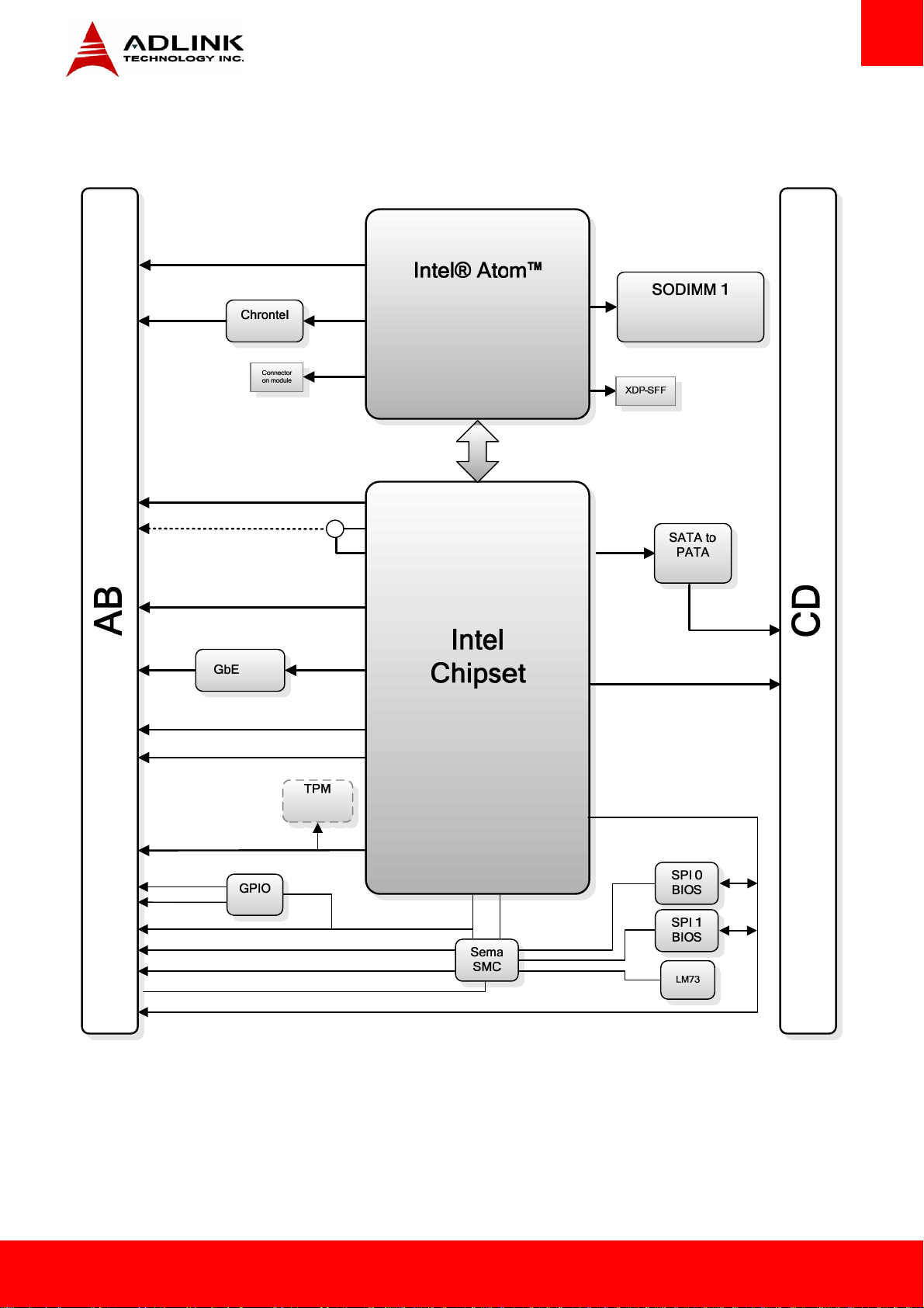
2.15. Functional Diagram
VGA
LVDS 24-bit
SATA 3Gb/s (port 0)
S
A
T
A
CH7511
3
(
s
/
b
G
3x PCIe x1
(port 0,1,2)
r
o
p
t
i210
8x USB 2.0
HDA Audio
)
1
eDP/DP
DP
PCIe x1
(port 3)
N2600
N2800
D2550
DMI
NM10
800/1067 MHz
1~4 GB DDR3
SATA
JM330
PATA
IDE
PCI Bus
ATMEL
AT97SC3204
4x GP0
4x GPI
SMbus
PCA9535
GP I2C
DDC I2C
s
C
L
P
b
u
SPI_CS0
SPI_CS1
SPI_CS#
SPI
Express-CVC Page 11
Page 12
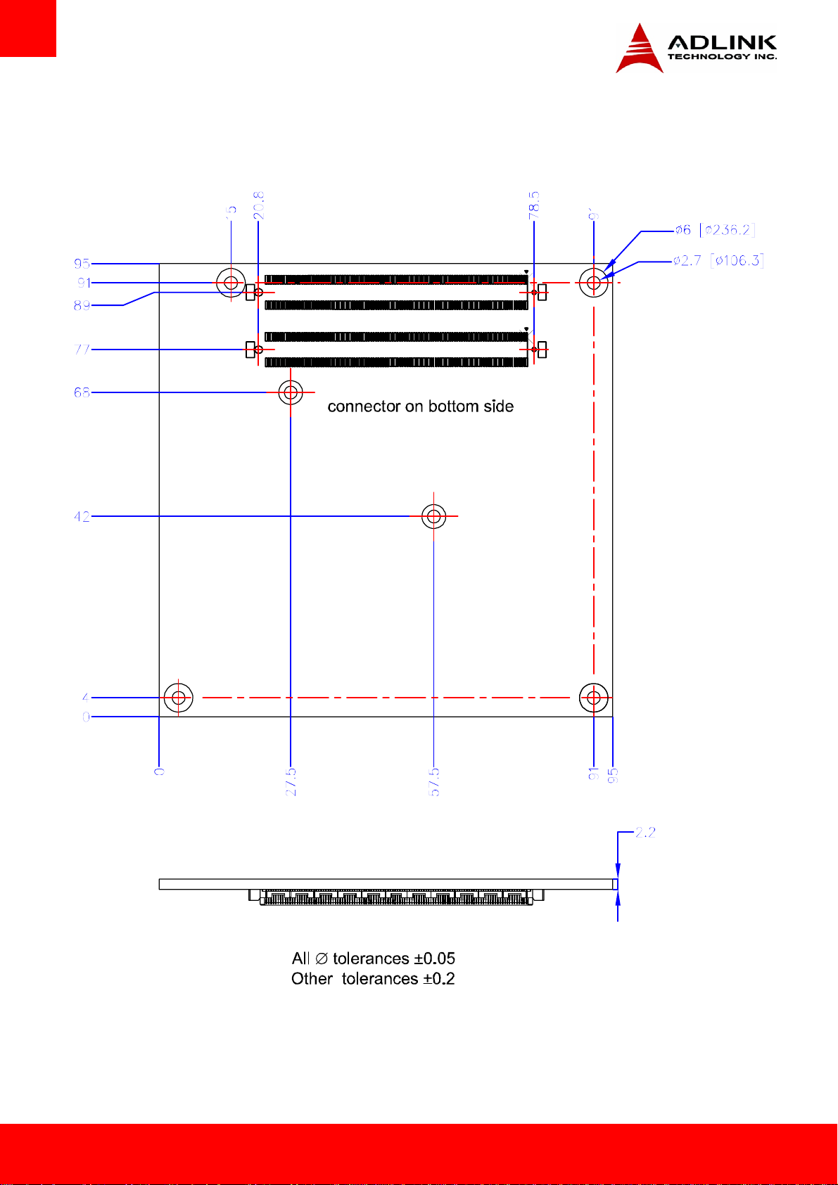
2.16. Mechanical Drawing
Page 12 Express-CVC
Page 13
3. COM Express Pinouts and Signal Descriptions
The following information is a summary of the most important information regarding pinout and signal description in the official PICMG
COM.0 Rev 2.0 (soon 2.1)
The pinout is noted here to emphazise issues that have not been followed in the past. The following might have small inacuaracies so in
case of doubt the offical design guide of PICMG should be consulted.
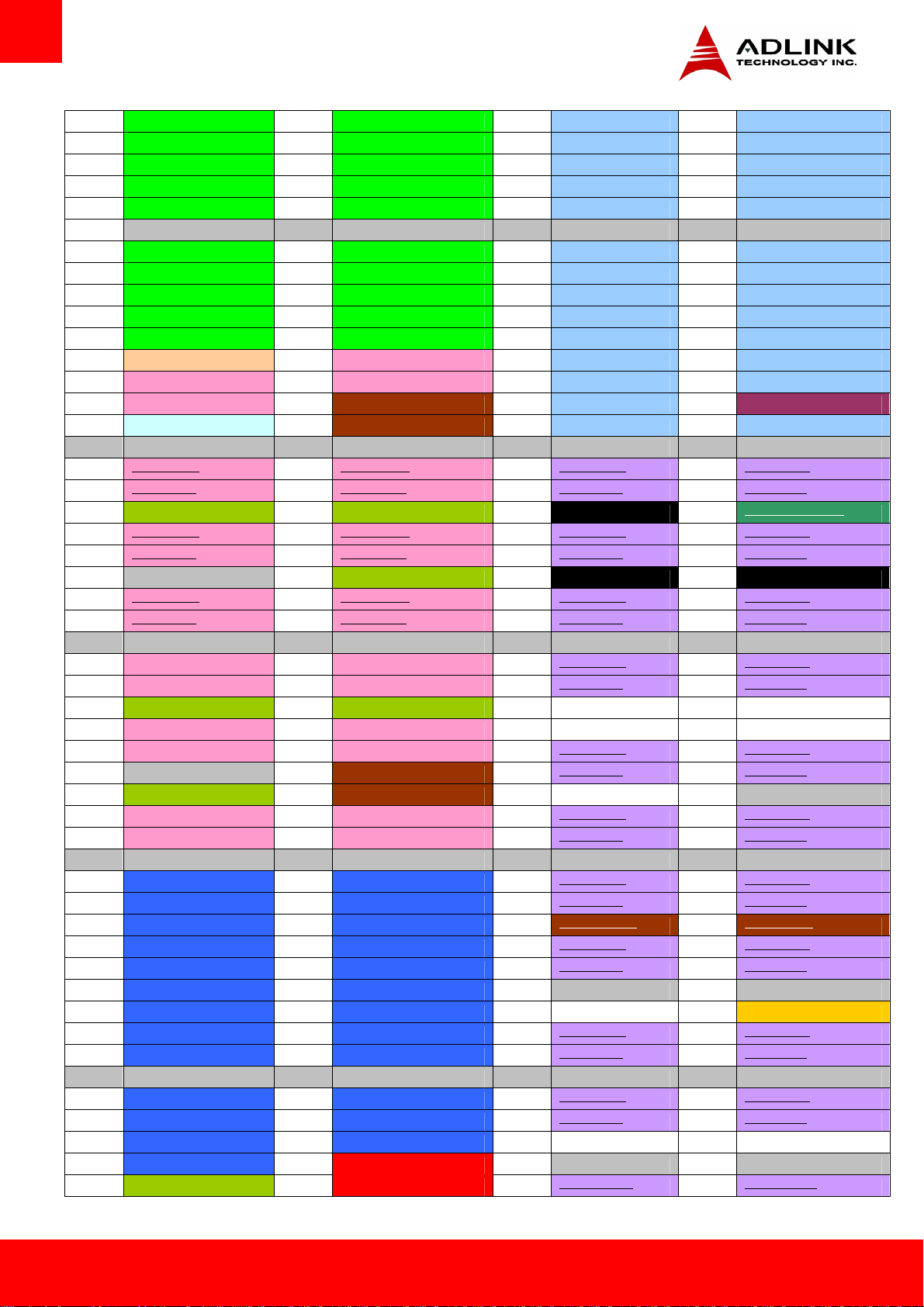
3.1. AB/CD Pin Definitions
The Express-CVC is a Type 2 module supporting PCI and PATA IDE on the CD connector.
All pins in the specification are described including those not supported on the Express-CVC.
Those not supported on the Express-CVC module are crossed out
Row A Row B Row C Row D
Pin Name Pin Name Pin Name Pin Name
A1 GND (FIXED) B1 GND (FIXED) C1 GND FIXED) D1 GND FIXED)
A2 GBE0_MDI3- B2 GBE0_ACT# C2 IDE_D7 D2 IDE_D5
A3 GBE0_MDI3+ B3 LPC_FRAME# C3 IDE_D6 D3 IDE_D10
A4 GBE0_LINK100# B4 LPC_AD0 C4 IDE_D3 D4 IDE_D11
A5 GBE0_LINK1000# B5 LPC_AD1 C5 IDE_D15 D5 IDE_D12
A6 GBE0_MDI2- B6 LPC_AD2 C6 IDE_D8 D6 IDE_D4
A7 GBE0_MDI2+ B7 LPC_AD3 C7 IDE_D9 D7 IDE_D0
A8 GBE0_LINK# B8 LPC_DRQ0# C8 IDE_D2 D8 IDE_REQ
A9 GBE0_MDI1- B9 LPC_DRQ1# C9 IDE_D13 D9 IDE_IOW#
A10 GBE0_MDI1+ B10 LPC_CLK C10 IDE_D1 D10 IDE_ACK#
A11 GND (FIXED) B11 GND (FIXED) C11 GND (FIXED) D11 GND (FIXED)
A12 GBE0_MDI0- B12 PWRBTN# C12 IDE_D14 D12 IDE_IRQ
A13 GBE0_MDI0+ B13 SMB_CK C13 IDE_IORDY D13 IDE_A0
A14 GBE0_CTREF B14 SMB_DAT C14 IDE_IOR# D14 IDE_A1
A15 SUS_S3# B15 SMB_ALERT# C15 PCI_PME# D15 IDE_A2
A16 SATA0_TX+ B16 SATA1_TX+ C16 PCI_GNT2# D16 IDE_CS1#
A17 SATA0_TX- B17 SATA1_TX- C17 PCI_REQ2# D17 IDE_CS3#
A18 SUS_S4# B18 SUS_STAT# C18 PCI_GNT1# D18 IDE_RESET#
A19 SATA0_RX+ B19 SATA1_RX+ C19 PCI_REQ1# D19 PCI_GNT3#
A20 SATA0_RX- B20 SATA1_RX- C20 PCI_GNT0# D20 PCI_REQ3#
A21 GND (FIXED) B21 GND (FIXED) C21 GND (FIXED) D21 GND (FIXED)
A22 SATA2_TX+ B22 SATA3_TX+ C22 PCI_REQ0# D22 PCI_AD1
A23 SATA2_TX- B23 SATA3_TX- C23 PCI_RESET# D23 PCI_AD3
A24 SUS_S5# B24 PWR_OK C24 PCI_AD0 D24 PCI_AD5
A25 SATA2_RX+ B25 SATA3_RX+ C25 PCI_AD2 D25 PCI_AD7
A26 SATA2_RX- B26 SATA3_RX- C26 PCI_AD4 D26 PCI_C/BE0#
A27 BATLOW# B27 WDT C27 PCI_AD6 D27 PCI_AD9
A28 (S)ATA_ACT# B28 AC/HDA_SDIN2 C28 PCI_AD8 D28 PCI_AD11
A29 AC/HDA_SYNC B29 AC/HDA_SDIN1 C29 PCI_AD10 D29 PCI_AD13
A30 AC/HDA_RST# B30 AC/HDA_SDIN0 C30 PCI_AD12 D30 PCI_AD15
A31 GND (FIXED) B31 GND (FIXED) C31 GND (FIXED) D31 GND (FIXED)
A32 AC/HDA_BITCLK B32 SPKR C32 PCI_AD14 D32 PCI_PAR
A33 AC/HDA_SDOUT B33 I2C_CK C33 PCI_C/BE1# D33 PCI_SERR#
A34 BIOS_DIS0# B34 I2C_DAT C34 PCI_PERR# D34 PCI_STOP#
A35 THRMTRIP# B35 THRM# C35 PCI_LOCK# D35 PCI_TRDY#
Express-CVC Page 13
Page 14
A36 USB6- B36 USB7- C36 PCI_DEVSEL# D36 PCI_FRAME#
A37 USB6+ B37 USB7+ C37 PCI_IRDY# D37 PCI_AD16
A38 USB_6_7_OC# B38 USB_4_5_OC# C38 PCI_C/BE2# D38 PCI_AD18
A39 USB4- B39 USB5- C39 PCI_AD17 D39 PCI_AD20
A40 USB4+ B40 USB5+ C40 PCI_AD19 D40 PCI_AD22
A41 GND (FIXED) B41 GND (FIXED) C41 GND (FIXED) D41 GND (FIXED)
A42 USB2- B42 USB3- C42 PCI_AD21 D42 PCI_AD24
A43 USB2+ B43 USB3+ C43 PCI_AD23 D43 PCI_AD26
A44 USB_2_3_OC# B44 USB_0_1_OC# C44 PCI_C/BE3# D44 PCI_AD28
A45 USB0- B45 USB1- C45 PCI_AD25 D45 PCI_AD30
A46 USB0+ B46 USB1+ C46 PCI_AD27 D46 PCI_IRQC#
A47 VCC_RTC B47 EXCD1_PERST# C47 PCI_AD29 D47 PCI_IRQD#
A48 EXCD0_PERST# B48 EXCD1_CPPE# C48 PCI_AD31 D48 PCI_CLKRUN#
A49 EXCD0_CPPE# B49 SYS_RESET# C49 PCI_IRQA# D49 PCI_M66EN GND)
A50 LPC_SERIRQ B50 CB_RESET# C50 PCI_IRQB# D50 PCI_CLK
A51 GND (FIXED) B51 GND (FIXED) C51 GND (FIXED) D51 GND (FIXED)
A52 PCIE_TX5+ B52 PCIE_RX5+ C52 PEG_RX0+ D52 PEG_TX0+
A53 PCIE_TX5- B53 PCIE_RX5- C53 PEG_RX0- D53 PEG_TX0-
A54 GPI0 B54 GPO1 C54 TYPE0# D54 PEG_LANE_RV#
A55 PCIE_TX4+ B55 PCIE_RX4+ C55 PEG_RX1+ D55 PEG_TX1+
A56 PCIE_TX4- B56 PCIE_RX4- C56 PEG_RX1- D56 PEG_TX1-
A57 GND B57 GPO2 C57 TYPE1# D57 TYPE2#
A58 PCIE_TX3+ B58 PCIE_RX3+ C58 PEG_RX2+ D58 PEG_TX2+
A59 PCIE_TX3- B59 PCIE_RX3- C59 PEG_RX2- D59 PEG_TX2-
A60 GND (FIXED) B60 GND (FIXED) C60 GND (FIXED) D60 GND (FIXED)
A61 PCIE_TX2+ B61 PCIE_RX2+ C61 PEG_RX3+ D61 PEG_TX3+
A62 PCIE_TX2- B62 PCIE_RX2- C62 PEG_RX3- D62 PEG_TX3-
A63 GPI1 B63 GPO3 C63 RSVD D63 RSVD
A64 PCIE_TX1+ B64 PCIE_RX1+ C64 RSVD D64 RSVD
A65 PCIE_TX1- B65 PCIE_RX1- C65 PEG_RX4+ D65 PEG_TX4+
A66 GND B66 WAKE0# C66 PEG_RX4- D66 PEG_TX4-
A67 GPI2 B67 WAKE1# C67 RSVD D67 GND
A68 PCIE_TX0+ B68 PCIE_RX0+ C68 PEG_RX5+ D68 PEG_TX5+
A69 PCIE_TX0- B69 PCIE_RX0- C69 PEG_RX5- D69 PEG_TX5-
A70 GND (FIXED) B70 GND (FIXED) C70 GND (FIXED) D70 GND (FIXED)
A71 LVDS_A0+ B71 LVDS_B0+ C71 PEG_RX6+ D71 PEG_TX6+
A72 LVDS_A0- B72 LVDS_B0- C72 PEG_RX6- D72 PEG_TX6-
A73 LVDS_A1+ B73 LVDS_B1+ C73 SDVO_DATA D73 SDVO_CLK
A74 LVDS_A1- B74 LVDS_B1- C74 PEG_RX7+ D74 PEG_TX7+
A75 LVDS_A2+ B75 LVDS_B2+ C75 PEG_RX7- D75 PEG_TX7-
A76 LVDS_A2- B76 LVDS_B2- C76 GND D76 GND
A77 LVDS_VDD_EN B77 LVDS_B3+ C77 RSVD D77 IDE_CBLID#
A78 LVDS_A3+ B78 LVDS_B3- C78 PEG_RX8+ D78 PEG_TX8+
A79 LVDS_A3- B79 LVDS_BKLT_EN C79 PEG_RX8- D79 PEG_TX8-
A80 GND (FIXED) B80 GND (FIXED) C80 GND (FIXED) D80 GND (FIXED)
A81 LVDS_A_CK+ B81 LVDS_B_CK+ C81 PEG_RX9+ D81 PEG_TX9+
A82 LVDS_A_CK- B82 LVDS_B_CK- C82 PEG_RX9- D82 PEG_TX9-
A83 LVDS_I2C_CK B83 LVDS_BKLT_CTRL C83 RSVD D83 RSVD
A84 LVDS_I2C_DAT B84 VCC_5V_SBY C84 GND D84 GND
A85 GPI3 B85 VCC_5V_SBY C85 PEG_RX10+ D85 PEG_TX10+
Page 14 Express-CVC
Page 15
A86 KBD_RST# B86 VCC_5V_SBY C86 PEG_RX10- D86 PEG_TX10-
A87 KBD_A20GATE B87 VCC_5V_SBY C87 GND D87 GND
A88 PCIE0_CK_REF+ B88 BIOS_DIS1# C88 PEG_RX11+ D88 PEG_TX11+
A89 PCIE0_CK_REF- B89 VGA_RED C89 PEG_RX11- D89 PEG_TX11-
A90 GND (FIXED) B90 GND (FIXED) C90 GND (FIXED) D90 GND (FIXED)
A91 SPI_POWER B91 VGA_GRN C91 PEG_RX12+ D91 PEG_TX12+
A92 SPI_MISO B92 VGA_BLU C92 PEG_RX12- D92 PEG_TX12-
A93 GPO0 B93 VGA_HSYNC C93 GND D93 GND
A94 SPI_CLK B94 VGA_VSYNC C94 PEG_RX13+ D94 PEG_TX13+
A95 SPI_MOSI B95 VGA_I2C_CK C95 PEG_RX13- D95 PEG_TX13-
A96 GND B96 VGA_I2C_DAT C96 GND D96 GND
A97 TYPE10# B97 SPI_CS# C97 RSVD D97 PEG_ENABLE#
A98 RSVD B98 RSVD C98 PEG_RX14+ D98 PEG_TX14+
A99 RSVD B99 RSVD C99 PEG_RX14- D99 PEG_TX14-
A100 GND (FIXED) B100 GND (FIXED) C100 GND (FIXED) D100 GND (FIXED)
A101 RSVD B101 RSVD C101 PEG_RX15+ D101 PEG_TX15+
A102 RSVD B102 RSVD C102 PEG_RX15- D102 PEG_TX15-
A103 RSVD B103 RSVD C103 GND D103 GND
A104 VCC_12V B104 VCC_12V C104 VCC_12V D104 VCC_12V
A105 VCC_12V B105 VCC_12V C105 VCC_12V D105 VCC_12V
A106 VCC_12V B106 VCC_12V C106 VCC_12V D106 VCC_12V
A107 VCC_12V B107 VCC_12V C107 VCC_12V D107 VCC_12V
A108 VCC_12V B108 VCC_12V C108 VCC_12V D108 VCC_12V
A109 VCC_12V B109 VCC_12V C109 VCC_12V D109 VCC_12V
A110 GND (FIXED) B110 GND (FIXED) C110 GND (FIXED) D110 GND (FIXED)
Express-CVC Page 15
Page 16

3.2. Signal Description Terminology
The following terms are used in the COM Express AB/CD Signal Descriptions below.
I Input to the Module
O Output from the Module
I/O Bi-directional input / output signal
OD Open drain output
I 3.3V Input 3.3V tolerant
I 5V Input 5V tolerant
O 3.3V Output 3.3V signal level
O 5V Output 5V signal level
I/O 3.3V Bi-directional signal 3.3V tolerant
I/O 5V Bi-directional signal 5V tolerant
I/O 3.3Vsb Input 3.3V tolerant active in standby state
P Power Input/Output
REF Reference voltage output that may be sourced from a module power plane.
PDS Pull-down strap. This is an output pin on the module that is either tied to GND or not connected.
The signal is used to indicate the PICMG module type to the Carrier Board.
PU ADLINK implemented pull-up resistor on module
PD ADLINK implemented pull-down resistor on module
Page 16 Express-CVC
Page 17
3.3. AB Signal Descriptions
3.3.1. Audio Signals
Signal Pin Description I/O PU/PD Comment
AC_RST# /
HDA_RST#
AC_SYNC /
HDA_SYNC
AC_BITCLK /
HDA_BITCLK
AC _SDOUT /
HDA_SDOUT
AC _SDIN[2:0]
HDA_SDIN[2:0]
A30 Reset output to CODEC, active low. O 3.3VSB
A29 Sample-synchronization signal to the CODEC(s). O 3.3V
A32 Serial data clock generated by the external
CODEC(s).
A33 Serial TDM data output to the CODEC. O 3.3V
B28B30
Serial TDM data inputs from up to 3 CODECs. I/O 3.3VSB
I/O 3.3V
3.3.2. Analog VGA
Signal Pin Description I/O PU/PD Comment
VGA_RED B89 Red for monitor.
Analog DAC output, designed to drive a
37.5-Ohm equivalent load.
VGA_GRN B91 Green for monitor.
Analog DAC output, designed to drive a
37.5-Ohm equivalent load.
O Analog If VGA is used than signal should be
pulled to GND by 150Ω on the carrier
O Analog If VGA is used than signal should be
pulled to GND by 150Ω on the carrier
VGA_BLU B92 Blue for monitor.
Analog DAC output, designed to drive a
37.5-Ohm equivalent load.
VGA_HSYNC B93 Horizontal sync output to VGA monitor O 3.3V
VGA_VSYNC B94 Vertical sync output to VGA monitor O 3.3V
VGA_I2C_CK B95 DDC clock line (I²C port dedicated to identify
VGA monitor capabilities)
VGA_I2C_DAT B96 DDC data line. I/O OD 3.3V PU 2k2 3.3V
O Analog If VGA is used than signal should be
I/O OD 3.3V PU 2k2 3.3V
pulled to GND by 150Ω on the carrier
Express-CVC Page 17
Page 18
3.3.3. LVDS
Signal Pin Description I/O PU/PD Comment
LVDS_A0+
LVDS_A0-
LVDS_A1+
LVDS_A1-
LVDS_A2+
LVDS_A2-
LVDS_A3+
LVDS_A3-
LVDS_A_CK+
LVDS_A_CK-
LVDS_B0+
LVDS_B0-
LVDS_B1+
LVDS_B1-
LVDS_B2+
LVDS_B2-
LVDS_B3+
LVDS_B3-
LVDS_B_CK+
LVDS_B_CK-
LVDS_VDD_EN A77 LVDS panel power enable O 3.3V
LVDS_BKLT_EN B79 LVDS panel backlight enable O 3.3V
LVDS_BKLT_CTRL B83 LVDS panel backlight brightness control O 3.3V
A71
A72
A73
A74
A75
A76
A78
A79
A81
A82
B71
B72
B73
B74
B75
B76
B77
B78
B81
B82
LVDS Channel A differential pairs O LVDS
LVDS Channel A differential clock O LVDS
LVDS Channel B differential pairs O LVDS
LVDS Channel B differential clock O LVDS
LVDS_I2C_CK A83 DDC lines used for flat panel detection and control. O 3.3V PU 2k2 3.3V
LVDS_I2C_DAT A84 DDC lines used for flat panel detection and control. I/O 3.3V
PU 2k2 3.3V
3.3.4. Gigabit Ethernet
Gigabit Ethernet Pin Description I/O PU/PD Comment
GBE0_MDI0+
GBE0_MDI0-
GBE0_MDI1+
GBE0_MDI1GBE0_MDI2+
GBE0_MDI2-
GBE0_MDI3+
GBE0_MDI3-
GBE0_ACT# B2 Gigabit Ethernet Controller 0 activity indicator, active low.
GBE0_LINK# A8 Gigabit Ethernet Controller 0 link indicator, active low.
GBE0_LINK100# A4 Gigabit Ethernet Controller 0 100Mbit/sec link indicator, active low.
GBE0_LINK1000# A5 Gigabit Ethernet Controller 0 1000Mbit/sec link indicator, active low.
A13
A11
A10
A9
A7
A6
A3
A2
Gigabit Ethernet Controller 0: Media Dependent Interface Differential
Pairs 0, 1, 2, 3. The MDI can operate in 1000, 100, and 10Mbit/sec
modes. Some pairs are unused in some modes according to the
following:
1000BASE-T 100BASE-TX 10BASE-T
MDI[0]+/- B1_DA+/- TX+/- TX+/-
MDI[1]+/- B1_DB+/- RX+/- RX+/-
MDI[2]+/- B1_DC+/MDI[3]+/- B1_DD+/-
I/O Analog Twisted
pair signals
for external
transformer
.
OD 3.3VSB PU 1k 3.3V
OD 3.3VSB
OD 3.3VSB
OD 3.3VSB
GBE0_CTREF A14 Reference voltage for Carrier Board Ethernet channel 1 and 2
magnetics center tap. The reference voltage is determined by the
requirements of the Module PHY and may be as low as 0V and as high
as 3.3V. The reference voltage output shall be current limited on the
Module. In the case in which the reference is shorted to ground, the
current shall be 250 mA or less.
GND min
3.3V max
Page 18 Express-CVC
Page 19
3.3.5. Serial ATA
Signal Pin Description I/O PU/PD Comment
SATA0_TX+
SATA0_TX-
SATA0_RX+
SATA0_RX-
SATA1_TX+
SATA1_TX-
SATA1_RX+
SATA1_RX-
SATA2_TX+
SATA2_TX-
SATA2_RX+
SATA2_RX-
SATA3_TX+
SATA3_TX-
SATA3_RX+
SATA3_RX-
(S)ATA_ACT# A28 ATA (parallel and serial) or SAS activity
A16
Serial ATA channel 0, Transmit Output
A17
differential pair.
A19
Serial ATA channel 0, Receive Input
A20
differential pair.
B16
Serial ATA channel 1, Transmit Output
B17
differential pair.
B19
Serial ATA channel 1, Receive Input
B20
differential pair.
A22
Serial ATA channel 2, Transmit Output
A23
differential pair.
A25
Serial ATA channel 2, Receive Input
A26
differential pair.
B22
Serial ATA channel 3, Transmit Output
B23
differential pair.
B25
Serial ATA channel 3, Receive Input
B26
differential pair.
indicator, active low.
O SATA AC coupled on Module
I SATA AC coupled on Module
O SATA AC coupled on Module
I SATA AC coupled on Module
O SATA Not supported
I SATA Not supported
O SATA Not supported
I SATA Not supported
O 3.3V
Express-CVC Page 19
Page 20
3.3.6. PCI Express
Signal Pin Description I/O PU/PD Comment
PCIE_TX0+
PCIE_TX0-
PCIE_RX0+
PCIE_RX0-
PCIE_TX1+
PCIE_TX1-
PCIE_RX1+
PCIE_RX1-
PCIE_TX2+
PCIE_TX2-
PCIE_RX2+
PCIE_RX2-
PCIE_TX3+
PCIE_TX3-
PCIE_RX3+
PCIE_RX3-
PCIE_TX4+
PCIE_TX4-
PCIE_RX4+
PCIE_RX4-
A68
A69
B68
B69
A64
A65
B64
B65
A61
A62
B61
B62
A58
A59
B58
B59
A55
A56
B55
B56
PCI Express channel 0, Transmit Output differential
pair.
PCI Express channel 0, Receive Input differential
pair.
PCI Express channel 1, Transmit Output differential
pair.
PCI Express channel 1, Receive Input differential
pair.
PCI Express channel 2, Transmit Output differential
pair.
PCI Express channel 2, Receive Input differential
pair.
PCI Express channel 3, Transmit Output differential
pair.
PCI Express channel 3, Receive Input differential
pair.
PCI Express channel 4, Transmit Output differential
pair.
PCI Express channel 4, Receive Input differential
pair.
O PCIE AC coupled on Module
I PCIE AC coupled off Module
O PCIE AC coupled on Module
I PCIE AC coupled off Module
O PCIE AC coupled on Module
I PCIE AC coupled off Module
O PCIE
I PCIE Not supported
O PCIE Not supported
I PCIE Not supported
Not supported
PCIE_TX5+
PCIE_TX5-
PCIE_RX5+
PCIE_RX5-
PCIE_CLK_REF+
PCIE_CLK_REF-
A52
A53
B52
B53
A88
A89
PCI Express channel 5, Transmit Output differential
pair.
PCI Express channel 5, Receive Input differential
pair.
PCI Express Reference Clock output for all PCI
Express and PCI Express Graphics Lanes.
O PCIE Not supported
I PCIE Not supported
O PCIE
3.3.7. Express Card
Signal Pin Description I/O PU/PD Comment
EXCD0_CPPE#
EXCD1_CPPE#
EXCD0_PERST#
EXCD1_PERST#
A49
B48
A48
B47
PCI ExpressCard: PCI Express capable card request I 3.3V PU 10k 3.3V
PCI ExpressCard: reset O 3.3V
Page 20 Express-CVC
Page 21

3.3.8. LPC bus
Signal Pin Description I/O PU/PD Comment
LPC_AD[0:3] B4-B7 LPC multiplexed address, command and data bus I/O 3.3V
LPC_FRAME# B3 LPC frame indicates the start of an LPC cycle O 3.3V
LPC_DRQ0#
LPC_DRQ1#
LPC_SERIRQ A50 LPC serial interrupt I/O OD 3.3V PU 8k2 3.3V
LPC_CLK B10 LPC clock output - 33MHz nominal O 3.3V
B8
B9
LPC serial DMA request I 3.3V
3.3.9. USB
Signal Pin Description I/O PU/PD Comment
USB0+
USB0-
USB1+
USB1-
USB2+
USB2-
USB3+
USB3-
USB4+
USB4-
USB5+
USB5-
A46
USB differential data pairs for Port 0 I/O 3.3VSB USB 1.1/ 2.0 compliant
A45
B46
USB differential data pairs for Port 1 I/O 3.3VSB USB 1.1/ 2.0 compliant
B45
A43
USB differential data pairs for Port 1 I/O 3.3VSB USB 1.1/ 2.0 compliant
A42
B43
USB differential data pairs for Port 2 I/O 3.3VSB USB 1.1/ 2.0 compliant
B42
A40
USB differential data pairs for Port 3 I/O 3.3VSB USB 1.1/ 2.0 compliant
A39
B40
USB differential data pairs for Port 4 I/O 3.3VSB USB 1.1/ 2.0 compliant
B39
USB6+
USB6-
USB7+
USB7-
USB_0_1_OC# B44 USB over-current sense, USB ports 0 and 1. A pull-up
USB_2_3_OC# A44 USB over-current sense, USB ports 2 and 3. A pull-up
USB_4_5_OC# B38 USB over-current sense, USB ports 4 and 5. A pull-up
USB_6_7_OC# A38 USB over-current sense, USB ports 6 and 7. A pull-up
A37
USB differential data pairs for Port 5 I/O 3.3VSB USB 1.1/ 2.0 compliant
A36
B37
USB differential data pairs for Port 6 I/O 3.3VSB USB 1.1/ 2.0 compliant
B36
for this line shall be present on the module. An open
drain driver from a USB current monitor on the carrier
board may drive this line low.
for this line shall be present on the module. An open
drain driver from a USB current monitor on the carrier
board may drive this line low. .
for this line shall be present on the module. An open
drain driver from a USB current monitor on the carrier
board may drive this line low.
for this line shall be present on the module. An open
drain driver from a USB current monitor on the carrier
board may drive this line low.
I 3.3VSB PU 10k 3.3VSB Do not pull high on carrier
I 3.3VSB PU 10k 3.3VSB Do not pull high on carrier
I 3.3VSB PU 10k 3.3VSB Do not pull high on carrier
I 3.3VSB PU 10k 3.3VSB Do not pull high on carrier
Express-CVC Page 21
Page 22
3.3.10. SPI (BIOS only)
Signal Pin Description I/O PU/PD Comment
SPI_CS# B97 Chip select for Carrier Board SPI BIOS Flash. O 3.3VSB
SPI_MISO A92 Data in to module from carrier board SPI BIOS flash. I 3.3VSB
SPI_MOSI A95 Data out from module to carrier board SPI BIOS flash. O 3.3VSB
SPI_CLK A94 Clock from module to carrier board SPI BIOS flash. O 3.3VSB
SPI_POWER A91 Power supply for Carrier Board SPI – sourced from Module
– nominally 3.3V.
The Module shall provide a minimum of 100mA on
SPI_POWER.
Carriers shall use less than 100mA of SPI_POWER.
SPI_POWER shall only be used to power SPI devices on
the Carrier
BIOS_DIS0# A34 Selection strap to determine the BIOS boot device. I PU 10K 3.3V Carrier shall pull to GND
BIOS_DIS1# B88 Selection strap to determine the BIOS boot device. I PU 10K 3.3V Carrier shall pull to GND
O P 3.3VSB
or leave not connected
or leave not connected
3.3.11. Miscellaneous
Signal Pin Description I/O PU/PD Comment
SPKR B32 Output for audio enunciator, the “speaker” in PC-AT
systems
WDT B27 Output indicating that a watchdog time-out event has
occurred.
KBD_RST# A86 Input to module from (optional) external keyboard
controller that can force a reset. Pulled high on the
module. This is a legacy artifact of the PC-AT.
O 3.3V
O 3.3V
I 3.3V PU 10K 3.3V
KBD_A20GATE A87 Input to module from (optional) external keyboard
controller that can be used to control the CPU A20 gate
line. The A20GATE restricts the memory access to the
bottom megabyte and is a legacy artifact of the PC-AT.
Pulled low on the module.
THRM# B35 Input from off-module temp sensor indicating an over-temp
situation.
THERMTRIP# A35 Active low output indicating that the CPU has entered
thermal shutdown.
TPM_PP11 C83 Trusted Platform Module (TPM) Physical Presence pin.
Active high. TPM chip has an internal pull down. This
signal is used to indicate Physical Presence to the TPM.
I 3.3V PU 10K 3.3V
I 3.3V
O 3.3V
I 3.3V PD 3.3V If TPM not installed on
module than remove PD
3.3V
Page 22 Express-CVC
Page 23

3.3.12. SMBus
Signal Pin Description I/O PU/PD Comment
SMB_CK B13 System Management Bus bidirectional clock line. Power
sourced through 5V standby rail and main power rails.
SMB_DAT# B14 System Management Bus bidirectional data line. Power
sourced through 5V standby rail and main power rails.
SMB_ALERT# B15 System Management Bus Alert – active low input can
be used to generate an SMI# (System Management
Interrupt) or to wake the system. Power sourced
through 5V standby rail and main power rails.
I/O OD 3.3VSB PU 2k2 3.3VSB
I/O OD 3.3VSB PU 2k2 3.3VSB
I 3.3VSB PU 10k 3.3VSB
3.3.13. I2C Bus
Signal Pin Description I/O PU/PD Comment
I2C_CK B33 General purpose I²C port clock output/input I/O OD 3.3VSB PU 2k2 3.3VSB
I2C_DAT B34 General purpose I²C port data I/O line I/O OD 3.3VSB PU 2k2 3.3VSB
3.3.14. General Purpose I/O (GPIO)
Signal Pin Description I/O PU/PD Comment
GPO[0] A93 General purpose output pins. O 3.3V
GPO[1] B54 General purpose output pins. O 3.3V
GPO[2] B57 General purpose output pins. O 3.3V
GPO[3] B63 General purpose output pins. O 3.3V
GPI[0] A54 General purpose input pins. Pulled high internally on the module. I 3.3V PU 10K 3.3V
GPI[1] A63 General purpose input pins. Pulled high internally on the module. I 3.3V PU 10K 3.3V
GPI[2] A67 General purpose input pins. Pulled high internally on the module. I 3.3V PU 10K 3.3V
GPI[3] A85 General purpose input pins. Pulled high internally on the module. I 3.3V PU 10K 3.3V
Express-CVC Page 23
Page 24

3.3.15. Power And System Management
Signal Pin Description I/O PU/PD Comment
PWRBTN# B12 Power button to bring system out of S5 (soft off), active on falling edge. I 3.3VSB PU 10k 3.3VSB
SYS_RESET# B49 Reset button input. Active low request for module to reset and reboot. May
be falling edge sensitive. For situations when SYS_RESET# is not able to
reestablish control of the system, PWR_OK or a power cycle may be used.
CB_RESET# B50 Reset output from module to Carrier Board. Active low. Issued by module
chipset and may result from a low SYS_RESET# input, a low PWR_OK
input, a VCC_12V power input that falls below the minimum specification, a
watchdog timeout, or may be initiated by the module software.
PWR_OK B24 Power OK from main power supply. A high value indicates that the power is
good. This signal can be used to hold off Module startup to allow carrier
based FPGAs or other configurable devices time to be programmed.
SUS_STAT# B18 Indicates imminent suspend operation; used to notify LPC devices. O 3.3VSB
SUS_S3# A15 Indicates system is in Suspend to RAM state. Active-low output. An inverted
copy of SUS_S3# on the carrier board (also known as “PS_ON”) may be
used to enable the non-standby power on a typical ATX power supply.
SUS_S4# A18 Indicates system is in Suspend to Disk state. Active low output. O 3.3VSB
SUS_S5# A24 Indicates system is in Soft Off state. O 3.3VSB
WAKE0# B66 PCI Express wake up signal. I 3.3VSB PU 10k 3.3VSB
WAKE1# B67 General purpose wake up signal. May be used to implement wake-up on
PS/2 keyboard or mouse activity.
BATLOW# A27 Battery low input. This signal may be driven low by external circuitry to signal
that the system battery is low, or may be used to signal some other external
power-management event.
I 3.3VSB PU 10k 3.3VSB
O 3.3VSB
I 3.3V
O 3.3VSB
I 3.3VSB PU 10k 3.3VSB
I 3.3VSB PU 10k 3.3VSB
Page 24 Express-CVC
Page 25

3.3.16. Power and Ground
Signal Pin Description I/O PU/PD Comment
VCC_12V A104-A109
B104-B109
VCC_5V_SBY B84-B87 Standby power input: +5.0V nominal. See section 7 “Electrical
VCC_RTC A47 Real-time clock circuit-power input. Nominally +3.0V. P
GND A1, A11, A21, A31,
A41, A51, A57, A66,
A80, A90, A96,
A100, A110, B1,
B11, B21 ,B31, B41,
B51, B60, B70, B80,
B90, B100, B110
Primary power input: +12V nominal (5 ~ 19V). See section 7
“Electrical Specifications“ for allowable input range. All available
VCC_12V pins on the connector(s) shall be used.
Specifications“ for allowable input range. If VCC5_SBY is used,
all available VCC_5V_SBY pins on the connector(s) shall be used.
Only used for standby and suspend functions. May be left
unconnected if these functions are not used in the system design.
Ground - DC power and signal and AC signal return path. P
P 5~20 V
P 5Vsb ±5%
Express-CVC Page 25
Page 26

3.4. CD Signal Descriptions
3.4.1. PATA IDE
Signal Pin Description I/O PU/PD Comment
IDE_D0
IDE_D1
IDE_D2
IDE_D3
IDE_D4
IDE_D5
IDE_D6
IDE_D7
IDE_D8
IDE_D9
IDE_D10
IDE_D11
IDE_D12
IDE_D13
IDE_D14
IDE_D15
IDE_A0 D13 Address lines to IDE device. O 3.3V
IDE_A1 D14 Address lines to IDE device. O 3.3V
IDE_A2 D15 Address lines to IDE device. O 3.3V
IDE_IOW# D9 I/O write line to IDE device. Data latched on trailing (rising)
IDE_IOR# C14 I/O read line to IDE device. O 3.3V
IDE_REQ D8 IDE Device DMA Request. It is asserted by the IDE device
IDE_ACK# D10 IDE Device DMA Acknowledge. O 3.3V
D7
C10
C8
C4
D6
D2
C3
C2
C6
C7
D3
D4
D5
C9
C12
C5
Bidirectional data to / from IDE device. I/O 3.3V
O 3.3V
edge.
I 3.3V
to request a data transfer.
IDE_CS1# D16 IDE Device Chip Select for 1F0h to 1FFh range. O 3.3V
IDE_CS3# D17 IDE Device Chip Select for 3F0h to 3FFh range. O 3.3V
IDE_IORDY C13 IDE device I/O ready input. Pulled low by the IDE device to
extend the cycle.
IDE_RESET# D18 Reset output to IDE device, active low.
IDE_IRQ D12 Interrupt request from IDE device. I 3.3V PD 10k shall
IDE_CBLID# D77 Input from off-module hardware indicating the type of IDE
cable being used. High indicates a 40-pin cable used for
legacy IDE modes. Low indicates that an 80-pin cable with
interleaved grounds is used. Such a cable is required for
Ultra-DMA 66, 100 and 133 modes.
I 3.3V PU 4k7 3.3V
O 3.3V
I 3.3V
Page 26 Express-CVC
Page 27

3.4.2. PCI
Signal Pin Description I/O PU/PD Comment
PCI_AD0
PCI_AD1
PCI_AD2
PCI_AD3
PCI_AD4
PCI_AD5
PCI_AD6
PCI_AD7
PCI_AD8
PCI_AD9
PCI_AD10
PCI_AD11
PCI_AD12
PCI_AD13
PCI_AD14
PCI_AD15
PCI_AD16
PCI_AD17
PCI_AD18
PCI_AD19
PCI_AD20
PCI_AD21
PCI_AD22
PCI_AD23
PCI_AD24
PCI_AD25
PCI_AD26
PCI_AD27
PCI_AD28
PCI_AD29
PCI_AD30
PCI_AD31
C24
PCI bus multiplexed address and data lines I/O 3.3V
D22
C25
D23
C26
D24
C27
D25
C28
D27
C29
D28
C30
D29
C32
D30
D37
C39
D38
C40
D39
C42
D40
C43
D42
C45
D43
C46
D44
C47
D45
C48
PCI_C/BE0#
PCI_C/BE1#
PCI_C/BE2#
PCI_C/BE3#
PCI_DEVSEL# C36 PCI bus Device Select, active low. I/O 3.3V PU 8k2 3.3V
PCI_FRAME# D36 PCI bus Frame control line, active low. I/O 3.3V PU 8k2 3.3V
PCI_IRDY# C37 PCI bus Initiator Ready control line, active low. I/O 3.3V PU 8k2 3.3V
PCI_TRDY# D35 PCI bus Target Ready control line, active low. I/O 3.3V PU 8k2 3.3V
PCI_STOP# D34 PCI bus STOP control line, active low, driven by cycle initiator. I/O 3.3V PU 8k2 3.3V
PCI_PAR D32 PCI bus parity I/O 3.3V
PCI_PERR# C34 Parity Error: An external PCI device drives PERR# when it
PCI_REQ0#
PCI_REQ1#
PCI_REQ2#
PCI_REQ3#
PCI_GNT0#
PCI_GNT1#
PCI_GNT2#
PCI_GNT3#
PCI_RESET# C23 PCI Reset output, active low. O 3.3V
D26
PCI bus byte enable lines, active low I/O 3.3V
C33
C38
C44
I/O 3.3V PU 8k2 3.3V
receives data that has a parity error.
C22
PCI bus master request input lines, active low. I 3.3V PU 8k2 3.3V
C19
C17
D20
C20
PCI bus master grant output lines, active low. O 3.3V
C18
C16
D19
Express-CVC Page 27
Page 28
PCI_LOCK# C35 PCI Lock control line, active low. I/O 3.3V PU 8k2 3.3V
PCI_SERR# D33 System Error: SERR# may be pulsed active by any PCI device
that detects a system error condition.
PCI_PME# C15 PCI Power Management Event: PCI peripherals drive PME# to
wake system from low-power states S1–S5.
PCI_CLKRUN# D48 Bidirectional pin used to support PCI clock run protocol for
mobile systems.
PCI_IRQA# PCI_IRQB#
PCI_IRQC# PCI_IRQD#
PCI_CLK D50 PCI 33MHz clock output O 3.3V
PCI_M66EN D49 Module input signal indicates whether an off-Module PCI device
C49
PCI interrupt request lines I 3.3V PU 8k2 3.3V
C50
D46
D47
is capable of 66MHz operation. Pulled to GND by Carrier Board
device or by Slot Card if the devices are NOT capable of 66
MHz operation.
If the Module is not capable of supporting 66 MHz PCI
operation, this input may be a no-connect on the Module.
If the Module is capable of supporting 66 MHz PCI operation,
and if this input is held low by the Carrier Board, the Module PCI
interface shall operate at 33 MHz.
I/O 3.3V PU 8k2 3.3V
I 3.3VSB
I/O 3.3V PU 10k 3.3V
Page 28 Express-CVC
Page 29

3.4.3. PCI Express Graphics x16 (PEG) or SDVO
PEG x16 Mode
Signal Pin Description I/O PU/PD Comment
PEG_RX0+
PEG_RX0-
PEG_RX1+
PEG_RX1-
PEG_RX2+
PEG_RX2-
PEG_RX3+
PEG_RX3-
PEG_RX4+
PEG_RX4-
PEG_RX5+
PEG_RX5-
PEG_RX6+
PEG_RX6-
PEG_RX7+
PEG_RX7-
PEG_RX8+
PEG_RX8-
PEG_RX9+
PEG_RX9-
PEG_RX10+
PEG_RX10-
PEG_RX11+
PEG_RX11-
PEG_RX12+
PEG_RX12-
PEG_RX13+
PEG_RX13-
PEG_RX14+
PEG_RX14-
PEG_RX15+
PEG_RX15
PEG_TX0+
PEG_TX0-
PEG_TX1+
PEG_TX1-
PEG_TX2+
PEG_TX2-
PEG_TX3+
PEG_TX3-
PEG_TX4+
PEG_TX4-
PEG_TX5+
PEG_TX5-
PEG_TX6+
PEG_TX6-
PEG_TX7+
PEG_TX7-
PEG_TX8+
PEG_TX8-
PEG_TX9+
PEG_TX9-
PEG_TX10+
PEG_TX10-
PEG_TX11+
PEG_TX11-
PEG_TX12+
PEG_TX12-
PEG_TX13+
PEG_TX13-
PEG_TX14+
C52
C53
C55
C56
C58
C59
C61
C62
C65
C66
C68
C69
C71
C72
C74
C75
C78
C79
C81
C82
C85
C86
C88
C89
C91
C92
C94
C95
C98
C99
C101
C102
D52
D53
D55
D56
D58
D57
D61
D62
D65
D66
D68
D69
D71
D72
D74
D75
D78
D79
D81
D82
D85
D86
D88
D89
D91
D92
D94
D95
D98
PCI Express Graphics transmit differential pairs. I PCIE Not supported
PCI Express Graphics receive differential pairs. O PCIE
Not supported
Express-CVC Page 29
Page 30

Signal Pin Description I/O PU/PD Comment
PEG_TX14-
PEG_TX15+
PEG_TX15-
PEG_LANE_RV# D54 PCI Express Graphics lane reversal input strap.
PEG_ENABLE# D97 Strap to enable PCI Express x16 external
D99
D101
D102
Pull low on the Carrier board to reverse lane
order.
graphics interface.
Pull low to enable the x16 interface.
I 1.05V
I 3.3V PU 10k 3.3V
Not supported
Not supported
SDVO Mode
Signal Pin Description I/O PU/PD Comment
SDVOB_RED+
SDVOB_RED-
SDVOB_GRN+
SDVOB_GRN-
SDVOB_BLU+
SDVOB_BLU-
SDVOB_CK+
SDVOB_CK-
SDVOB_INT+
SDVOB_INT-
SDVOC_RED+
SDVOC_RED-
SDVOC_GRN+
SDVOC_GRN-
SDVOC_BLU+
SDVOC_BLU-
SDVOC_CK+
SDVOC_CK-
SDVOC_INT+
SDVOC_INT-
SDVO_TVCLKIN+
SDVO_TVCLKIN-
SDVO_FLDSTALL+
SDVO_FLDSTALL-
SDVO_I2C_CK D73 SDVO I²C clock line to set up SDVO peripherals. I/O OD 2.5V
D52
Serial Digital Video B red output differential pair.
D53
Multiplexed with PEG_TX[0]+ and PEG_TX[0]- pair.
D55
Serial Digital Video B green output differential pair.
D56
Multiplexed with PEG_TX[1]+ and PEG_TX[1]-.
D58
Serial Digital Video B blue output differential pair.
D59
Multiplexed with PEG_TX[2]+ and PEG_TX[2]-.
D61
Serial Digital Video B clock output differential pair.
D62
Multiplexed with PEG_TX[3]+ and PEG_TX[3]-.
C55
Serial Digital Video B interrupt input differential pair.
C56
Multiplexed with PEG_RX[1]+ and PEG_RX[1]-.
D65
Serial Digital Video C red output differential pair.
D66
Multiplexed with PEG_TX[4]+ and PEG_TX[4]-.
D68
Serial Digital Video C green output differential pair.
D69
Multiplexed with PEG_TX[5]+ and PEG_TX[5]-.
D71
Serial Digital Video C blue output differential pair.
D72
Multiplexed with PEG_TX[6]+ and PEG_TX[6]-.
D74
Serial Digital Video C clock output differential pair.
D75
Multiplexed with PEG_TX[7]+ and PEG_TX[7]-.
C68
Serial Digital Video C interrupt input differential pair.
C69
Multiplexed with PEG_RX[5]+ and PEG_RX[5]-.
C52
Serial Digital Video TVOUT synchronization clock input
C53
differential pair. Multiplexed with PEG_RX[0]+ and PEG_RX[0]-.
C58
Serial Digital Video Field Stall input differential pair.
C59
Multiplexed with PEG_RX[2]+ and PEG_RX[2]-.
O PCIE
O PCIE
O PCIE
O PCIE
I PCIE
O PCIE
O PCIE
O PCIE
O PCIE
I PCIE
I PCIE
I PCIE
Not supported
Not supported
Not supported
Not supported
Not supported
Not supported
Not supported
Not supported
Not supported
Not supported
Not supported
Not supported
Not supported
SDVO_I2C_DAT C73 SDVO I²C data line to set up SDVO peripherals. I/O OD 2.5V
Not supported
Page 30 Express-CVC
Page 31

3.4.4. Module Type Definition
Pin Pin
Name
TYPE0#
TYPE1#
TYPE2#
C54
C57
D57
SDVO DP HDMI \ DVI
The TYPE pins indicate to the Carrier Board the Pin-out Type that is implemented on the
module. The pins are tied on the module to either ground (GND) or are no-connects (NC). For
Pinout Type 1, these pins are don’t care (X).
TYPE2# TYPE1# TYPE0#
X X X Pinout Type 1
NC NC NC Pinout Type 2
NC NC GND Pinout Type 3 (no IDE)
NC GND NC Pinout Type 4 (no PCI)
NC GND GND Pinout Type 5 (no IDE, no PCI)
GND NC NC Pinout Type 6 (no IDE, no PCI)
The Carrier Board should implement combinatorial logic that monitors the module TYPE pins
and keeps power off (e.g deactivates the ATX_ON signal for an ATX power supply) if an
incompatible module pin-out type is detected. The Carrier Board logic may also implement a
fault indicator such as an LED.
This is a Type 2
module
3.4.5. Power and Ground
Signal Pin Description I/O PU/PD Comment
VCC_12V C104-C109
D104-D109
Primary power input: +12V nominal. All available VCC_12V pins on
the connector(s) shall be used.
P 5~20 V
GND C1, C11, C21, C31, C41,
C51, C60, C70, C76, C80,
C84, C87, C90, C93, C96,
C100, C103, C110, D1,
D11, D21, D31, D41, D51,
D60, D67, D70, D76, D80,
D84, D87, D90, D93, D96,
D100, D103, D110
Ground - DC power and signal and AC signal return path.
All available GND connector pins shall be used and tied to carrier
board GND plane.
P
Express-CVC Page 31
Page 32

4. Non PICMG Connectors on the Module
This connector is a low height flex-edge connector. The overall board real estate required is significantly smaller than the 60-pin XDP debug
port connector. Compared to the 60-pin XDP debug port connector, the 26-pin XDP-SFF connector supports fewer DFX features. This is the
connector recommended for OEM/ODM designs. The 26-pin XDP-SFF debug port supports the following features on a Next Generation
Intel® Atom® Processor based Desktop and Mobile Platform:
• JTAG
• Run Control through dedicated PREQ/PRDY pins
• Reset and Powergood recovery and request signals.
Pin XDP Signal Name Target Signal I/O Pin XDP Signal Name Target Signal I/O
1 OBSFN_A0 PREQ#/BPM[5] O 2 OBSFN_A1 PRDY#/BP M[4] I
3 GND GND NA 4 OBSDTA_A[0] Open NA
5 OBSDATA_A[1] Open NA 6 GND GND NA
7 OBSDATA_A[2] Open NA 8 OBSDATA_A[3] Open NA
9 GND GND NA 10 HOOK0 PWROK I
11 HOOK1 PWRGOOD_REQ O 12 HOOK2 RSVD_K26 (optional) NA
13 HOOK3 Open I 14 HOOK4 Open NA
15 HOOK5 Open I 16 VCCOBS_AB VCC_CPU NA
17 HOOK6 RESET# I 18 HOOK7 DBR# O
19 GND GND NA 20 TDO TDO I
21 TRSTn TRSTn O 22 TDI TDI O
23 TMS TMS O 24 TCK1 Open
25 GND GND NA 26 TCK0 TCK0 O
For design information, refer to Intel Document: Debug Port Design Guide, Intel Document Number 492419.
Page 32 Express-CVC
Page 33

5. System Resources
5.1. System Memory Map
Address Range (decimal) Address Range (hex) Size Description
(4GB-2MB) FFE00000 – FFFFFFFF 2 MB High BIOS Area
(4GB-18MB) – (4GB-17MB-1) FEE00000 – FEEFFFFF 1 MB FSB Interrupt Memory Space
(4GB-20MB) – (4GB-19MB-1) FEC00000 – FECFFFFF 1 MB APIC Configuration Space
960 K – 1024 K F0000 – FFFFF 64 KB System BIOS Area
896 K – 960 K E0000 – EFFFF 64 KB Extended System BIOS Area
768 K – 896 K C0000 – DFFFF 128 KB Onboard VGA BIOS ROM
Intel i210 PXE ROM
640 K – 768 K A0000 – BFFFF 128 KB Legacy Video Buffer Area
0 K – 640 K 00000 – 9FFFF 640 KB DOS Area
5.2. Direct Memory Access Channels
Channel Number Data Width System Resource
0 8-bits Generic
1 8-bits Generic
2 8-bits Generic
3 8-bits Generic
4 Reserved - cascade channel
5 16-bits Generic
6 16-bits Generic
7 16-bits Generic
Note: These IRQs can be used for PCI devices when onboard device is disabled
Express-CVC Page 33
Page 34

5.3. I/O Map
Hex Range Device
000-01F DMA controller
020-02D and 030-03F Interrupt controller
02E-02F LPC SIO configuration index/data registers
040-05F Timer
060, 062, 064, 066 Keyboard
061, 063, 065, 067 NMI control and status
070-07F Real Time Clock Controller( bit 7 -NMI mask)
080-091 DMA controller
092 Reset (Bit 0)/ Fast Gate A20 (Bit 1)
93-9F DMA controller
0A0-0B1 and 0B4-0BF Interrupt controller
0B2h APM Control I/O Address
0B3h APM Status I/O Address
0C0-0DF DMA controller
0F0 Co-processor error register
180-181 Default AIM4 SRAM control register (May be remapped)
182-1EF Available
1F0-1F7 Primary IDE Controller (AT Drive)
1FB-22F Available
230 -277 Available
278-27F Reserved for parallel port
280-2F7 Available
2F8-2FF Serial Port 2
300-36F Available
370-377 Alt. Floppy Disk Controller
378-37F Reserved for parallel port
380-3AF Available
3B0-3BB and 3BF Mono/VGA mode video
3BC-3BE Reserved for parallel port
3C0-3DF VGA registers
3E0-3EF Available
3F0-3F7 Primary Floppy disk controller
3F8-3FF Serial port 1
4D0 Master PIC Edge/Level Trigger register
4D1 Slave PIC Edge/Level Trigger register
CF8-CFB PCI configuration address register (32 bit I/O only)
CF9 Reset Control register (8 bit I/O)
Page 34 Express-CVC
Page 35

Hex Range Device
CFC-CFF PCI configuration data register
F00 Smbus base address for SB.
500 GPIO Base Address for SB
400 PM (ACPI) Base Address for SB
460 Alias for ICH TCO base address.
0A00~0AFF Reserved for SIO functions base address (ex: PME /GPIO etc)
000-01F DMA controller
020-02D and 030-03F Interrupt controller
5.4. Interrupt Request (IRQ) Lines
PIC Mode
IRQ# Typical Interrupt Resource Connected to Pin Available
0 Counter 0 N/A No
1 Keyboard controller IRQ1 via SERIRQ No
2 Cascade interrupt from slave PIC N/A No
3 Serial Port 2 IRQ3 via SERIRQ / PIRQ Note
4 Serial Port 1 IRQ4 via SERIRQ / PIRQ Note
5 Generic Generic No
6 Floppy Drive Controller IRQ6 via SERIRQ / PIRQ Note
7 Generic IRQ7 via SERIRQ / PIRQ Note
8 Real-time clock N/A No
9 Generic IRQ9 via SERIRQ / PIRQ Note
10 Generic IRQ10 via SERIRQ / PIRQ Note
11 Generic IRQ11 via SERIRQ / PIRQ Note
12 PS/2 Mouse / PCI IRQ12 via SERIRQ / PIRQ Note
13 Internal N/A No
14 Primary IDE controller / PCI IRQ14 via SERIRQ / PIRQ Note
15 Secondary IDE controller / PCI IRQ15 via SERIRQ / PIRQ Note
Note: These IRQs can be used for PCI devices when onboard device is disabled
Express-CVC Page 35
Page 36

APIC Mode
IRQ# Typical Intterupt Resource Connected to Pin Available
0 Counter 0 N/A No
1 Keyboard controller N/A No
2 Cascade interrupt from slave PIC N/A No
3 Serial Port 2 (COM2) / PCI IRQ3 via SERIRQ / PIRQ Note
4 Serial Port 1 (COM1) / PCI IRQ4 via SERIRQ / PIRQ Note
5 Generic Generic No
6 Floppy Drive Controller IRQ6 via SERIRQ / PIRQ Note
7 Smbus Controller SMBus Controller / PIRQ Note
8 Real-time clock N/A No
9 Generic IRQ9 via SERIRQ / PIRQ Note
10 Generic IRQ10 via SERIRQ / PIRQ Note
11 Ethernet Controller IRQ11 via SERIRQ / PIRQ Note
12 PS/2 Mouse / PCI IRQ12 via SERIRQ / PIRQ Note
13 Math Processor N/A No
14 Primary IDE controller / PCI IRQ14 via SERIRQ / PIRQ Note
15 Secondary IDE controller / PCI IRQ15 via SERIRQ / PIRQ Note
16 N/A PCIE Port 0/1/2/3 UHCI Controller 3, P.E.G Root Port,
I.G.D,PCI Slot0/1
17 N/A PCIE Port 0/1/2/3, P.E.G Root Port, PCI Slot 0/1 Yes
18 N/A PCIE Port 0/1/2/3 UHCI Controller 2, P.E.G Root Port, SATA
Host controller, PCI Slot 0/1
19 N/A PCIE Port 0/1/2/3 UHCI Controller 1, P.E.G Root Port, SATA
Host controller, SMBus Controller ,PCI Slot 0/1
20 N/A NM10 internal GBE controller No
21 N/A N/A No
22 N/A HDA No
23 N/A UHCI Controller 0, EHCI Controller 1 No
Yes
Yes
Yes
Note: These IRQs can be used for PCI devices when onboard device is disabled
Page 36 Express-CVC
Page 37

5.5. PCI Configuration Space Map
Bus
Number
00h 00h 00h N/A Intel Host Processor Bridge
00h 02h 00h Internal Intel P.E.G. Root Port
00h 1Bh 00h Internal Intel HD Audio Device
00h 1Ch 00h Internal Intel PCI Express Root Ports 0
00h 1Ch 01h Internal Intel PCI Express Root Ports 1
00h 1Ch 02h Internal Intel PCI Express Root Ports 2
00h 1Ch 03h Internal Intel PCI Express Root Ports 3
00h 1Dh 00h Internal Intel USB UHCI Host Controllers 0
00h 1Dh 01h Internal Intel USB UHCI Host Controllers 1
00h 1Dh 02h Internal Intel USB UHCI Host Controllers 2
00h 1Dh 03h Internal Intel USB UHCI Host Controllers 3
00h 1Dh 07h Internal Intel USB EHCI Host Controller
00h 1Eh 00h N/A Intel PCI-to-PCI Bridge
00h 1Fh 00h N/A Intel LPC Interface Bridge
00h 1Fh 02h Internal Intel SATA controller
Device
Number
Function
Number
Routing Description
00h 1Fh 03h Internal Intel SMBus Controller
02h 00h 00h Internal Intel Ethernet Controller
Express-CVC Page 37
Page 38

5.6. PCI Interrupt Routing Map
INT
Line
INT0 INTA:16 INTH:23 INTH:23 INTG:22
INT1 INTD:19 INTD:19 INTD:19
INT2 INTC:18
INT3 INTA:16
P.E.G
Root Port
SATA
Controller
SMBUS
Controller
UHCI 0 UHCI 1 UHCI 2 UHCI 3 EHCI
Controller
#1
HDA
Controller
INT
Line
INT0 INTA:16 INTB:17 INTD:19 INTA:16
INT1 INTB:17 INTC:18 INTA:16 INTB:17
INT2 INTC:18 INTD:19 INTB:17 INTC:18
INT3 INTD:19 INTA:16 INTC:18 INTD:19
PCIE Port 0 PCIE Port 1 PCIE Port 2 GbE
Controller
5.7. SMBus
Device Address
DIMM A A0h SO-DIMM
Extend GPIO PCA9535BS 40h
The System Management (SM) bus originates from to the Intel NM10 PCH Smbus controller and connects to critical devices on the module.
It is not recommended to use this bus for off module devices.
.
5.8. I2C bus
The I2C bus is not occupied by any on module devices
Page 38 Express-CVC
Page 39

6. BIOS Setup
The following chapter describes basic navigation for the AMIBIOS®EFI BIOS setup utility.
6.1. Starting the BIOS
To enter the setup screen, follow these steps:
1. Power on the motherboard
2. Press the < Delete > key on your keyboard when you see the following text prompt: < Press DEL to run Setup >
3. After you press the < Delete > key, the main BIOS setup menu displays. You can access the other setup screens from the main
BIOS setup menu, such as Chipset and Power menus.
In most cases, the < Delete > key is used to invoke the setup screen. There are several cases that use other keys, such as <
F1 >, < F2 >, and so on.
Express-CVC Page 39
Page 40

6.1.1. Setup Menu
The main BIOS setup menu is the first screen that you can navigate. Each main BIOS setup menu option is described in this user’s guide.
The Main BIOS setup menu screen has two main frames. The left frame displays all the options that can be configured. “Grayed” options
cannot be configured, “Blue” options can be.
The right frame displays the key legend. Above the key legend is an area reserved for a text message. When an option is selected in the left
frame, it is highlighted in white. Often a text message will accompany it.
Page 40 Express-CVC
Page 41

6.1.2. Navigation
The BIOS setup/utility uses a key-based navigation system called hot keys. Most of the BIOS setup utility hot keys can be used at any time
during the setup navigation process. These keys include < F1 >, < F10 >, < Enter >, < ESC >, < Arrow > keys, and so on.
There is a hot key legend located in the right frame on most setup screens.
→← Left/Right. The Left and Right < Arrow > keys allow you to select a setup screen.
For example: Main screen, Advanced screen, Chipset screen, and so on.
↑↓ Up/Down The Up and Down < Arrow > keys allow you to select a setup item or sub-screen.
+- Plus/Minus The Plus and Minus < Arrow > keys allow you to change the field value of a particular setup item.
For example: Date and Time.
Tab The < Tab > key allows you to select setup fields.
Express-CVC Page 41
Page 42

Hot Key Description
Enter The < Enter > key allows you to display or change the setup option listed for a particular setup item. The < Enter
> key can also allow you to display the setup sub-screens.
F1 The < F1 > key allows you to display the General Help screen.
Press the < F1 > key to open the General Help screen.
F2 The < F2 > key on your keyboard is the previous values key. It is not displayed on the key legend by default. To set
the previous values settings of the BIOS, press the < F2 > key on your keyboard. It is located on the upper row of a
standard 101 keyboard. The previous values settings allow the motherboard to boot up with the least amount of
options set. This can lessen the probability of conflicting settings.
Press the < Enter > key to load previous values. You can also use the < Arrow > key to select Cancel and then
press the < Enter > key to abort this function and return to the previous screen.
F3 The < F3 > key on your keyboard is the optimized defaults key. To set the optimized defaults settings of the BIOS,
press the < F3 > key on your keyboard. It is located on the upper row of a standard 101 keyboard. The optimized
defaults settings allow the motherboard to boot up with the optimized defaults of options set. This can lessen the
probability of conflicting settings.
Press the < Enter > key to load optimized defaults. You can also use the < Arrow > key to select Cancel and then
press the < Enter > key to abort this function and return to the previous screen.
Page 42 Express-CVC
Page 43

F4 The < F4 > key allows you to save any changes you have made and exit Setup. Press the < F4 > key to save your
changes. The following screen will appear:
Press the < Enter > key to save the configuration and exit. You can also use the < Arrow > key to select Cancel
and then press the < Enter > key to abort this function and return to the previous screen.
ESC The < Esc > key allows you to discard any changes you have made and exit the Setup. Press the < Esc > key to
exit the setup without saving your changes. The following screen will appear:
Press the < Enter > key to discard changes and exit. You can also use the < Arrow > key to select Cancel and then
press the < Enter > key to abort this function and return to the previous screen.
Express-CVC Page 43
Page 44

6.2. Main Setup
Page 44 Express-CVC
Page 45

6.2.1. System Management
Power-Up Mode
Turn On:The machine starts automatically when the power supply is turned on.
Remain Off: To start the machine the power button has to be pressed.
Last State:The machine will return to the last state on power up.
ECO Mode
Reduces the power consumption of the system.
Express-CVC Page 45
Page 46

Power-Up Watchdog
The Power-Up Watchdog resets the system after a certain amount of time after power-up.
System & Board Info
The Main BIOS setup screen reports board information.
¾ Project Version
Displays the current BIOS version.
¾ Build Data
Displays the BIOS build data.
System Date/System Time
Use this option to change the system time and date. Highlight System Time or System Date using the < Arrow > keys. Enter new values
using the keyboard. Press the < Tab > key or the < Arrow > keys to move between fields. The date must be entered in MM/DD/YY format.
The time is entered in HH:MM:SS format.
The time is in 24-hour format. For example, 5:30 A.M. appears as 05:30:00, and 5:30 P.M. as 17:30:00.
Page 46 Express-CVC
Page 47

6.3. Advanced Setup
6.3.1. PCI Subsystem Settings
PCI Latency Timer
Value to be programmed into the PCI Latency Timer Register.
VGA Palette Snoop
Enables or Disables VGA Palette Registers Snooping.
PERR# Generation
Enables or Disables PCI Device to Generate PERR#.
SERR# Generation
Enables or Disables PCI Device to Generate SERR#.
Express-CVC Page 47
Page 48

6.3.2. ACPI Settings
Enable APIC Auto Configuration
BIOS ACPI Auto Configuration. Set this value to Enabled/Disabled.
Enable Hibernation
Controls system's ability to hibernate (OS/S4 Sleep State). Set this value to Enabled/Disabled.
ACPI Sleep State
Select the highest ACPI sleep state the system will enter, when the SUSPEND button is pressed. Set this value to Suspend Disable, S1, S3,
Both S1 and S3.
S1 only(CPU Stop Clock)
CPU Stop Clock - Under this setting the system enters a low power state instead of being completely shut off. This allows the
computer system to boot up in a few seconds.
S3 only(Suspend)
Suspend to RAM - Under this setting the system enters a low power state instead of being completely shut off. This allows the
computer system to boot up in a few seconds.
Emulation AT/ATX
Select Emulation AT or ATX function.If this option set to [Emulation AT], BIOS will report no suspend functions to ACPI OS. In Windows XP,
it will make the OS show a shutdown message during system shutdown.
Page 48 Express-CVC
Page 49

6.3.3. Trusted Computing
Security Device Support
Enables or Disables BIOS support for security device. OS will not show Security Device.TCG EFI protocol and INT1A interface will not be
available.
6.3.4. CPU Configuration
Hyper-threading
Enabled for Windows XP and Linux (OS optimized for Hyper-Threading Technology) and Disabled for other OS (OS not optimized for HyperThreading Technology). When disabled, only one thread per enabled core is enabled.
Express-CVC Page 49
Page 50

Execute Disable Bit
XD can prevent certain classes of malicious buffer overflow attacks when combined with a supporting OS (Windows Server 2003 SP1,
Windows XP SP2, SuSE Linux 9.2, Red Hat Enterprise 3 Update 3.)
Limit CPUID Maximum
When the computer boots, the operating system executes its CPUID instruction to identify the processor and its capabilities. Before it can do
so, it must first query the processor to find out the highest input value the CPUID recognizes. This determines the kind of basic information
CPUID can provide the operating system. This option allows you to circumvent problems with older operating systems.
When enabled, the processor will limit the maximum CPUID input value to 03h when queried, even if the processor supports a higher CPUID
input value. When Disabled, the processor will return the actual maximum CPUID input value of the processor when queried.
6.3.5. Thermal Configuration
Page 50 Express-CVC
Page 51

CPU Thermal Configuration
DTS SMM
Enabled: ACPI thermal management uses DTS SMM mechanism to obtain CPU temperature values.
CPU Temperature
Display current CPU temperature.
Express-CVC Page 51
Page 52

Platform Thermal Configuration
Critical Trip Point
This value controls the temperature of the ACPI Critical Trip Point - the point at which the OS will shut the system off. NOTE:
100°C is the Plan of Record (POR) for all Intel mobile processors.
Active Trip Point Lo Fan Speed
This value controls the temperature of the ACPI Active Trip Point - the point at which the OS will turn the processor fan to low.
Active Trip Point Hi Fan Speed
This value controls the temperature of the ACPI Active Trip Point - the point at which the OS will turn the processor fan to high.
Passive Trip Point
This value controls the temperature of the ACPI Passive Trip Point - the point at which the OS will begin throttling the processor.
Page 52 Express-CVC
Page 53

6.3.6. IDE Configuration
SATA Controller(s)
Enables or disables SATA Controller.
SATA-to-PATA controller
Enable if system uses PATA drive; Disable will reduce hard drive detection time when no PATA drive.
Note: To use two SATA ports (SATA0/1), this setting must be enabled
Configure SATA as
Select a configuration IDE/AHCI for SATA Controller.
Express-CVC Page 53
Page 54

Configure SATA as “AHCI”
Port0/1 Speed Limit
Select Port0/1 AHCI Speed Limit.
SATA Port 0/1
Enable or Disable SATA Port 0/1.
SATA Port 0/1 Hot Plug
Designates this port 0/1 as hot pluggable.
Page 54 Express-CVC
Page 55

6.3.7. USB Configuration
Legacy USB Support
Enables Legacy USB support. AUTO option, disables legacy support if no USB devices are connected. DISABLE option will keep USB
devices available only for EFI applications. Set this value to Enable/Disable/Auto.
EHCI Hand-off
This is a workaround for OSes without EHCI hand-off support. The EHCI ownership change should be claimed by EHCI driver. Set this value
to Enabled/Disabled.
USB transfer time-out
The time-out value for Control, Bulk, and Interrupt transfers. Set this value to 1 sec / 5 sec / 10 sec / 20 sec.
Device reset time-out
USB mass storage device Start Unit command time-out. Set this value to 10 sec / 20 sec / 30 sec / 40 sec.
Device power-up delay
Maximum time the device will take before it properly reports itself to the Host Controller. 'Auto' uses default value: for a Root port it is 100 ms,
for a Hub port the delay is taken from Hub descriptor. Set this value to Auto/Manual.
Express-CVC Page 55
Page 56

6.3.8. W8362DHG Super IO Configuration
Floppy Disk Controller Configuration
Change Settings
This option specifies the base I/O port address and interrupt request address of serial port 0,1 (COMA,B). Configuration options:
Auto, 3F0.
Page 56 Express-CVC
Page 57

Device Mode
Change mode of Floppy Disk Controller. Select 'Read Write' for normal operation. Select 'Write Protect' mode for read only
operation.
Serial Port 0/1 Configuration
Set Parameters of Serial Port 0/1 (COMA/B)
Change Settings
This option specifies the base I/O port address and interrupt request address of serial port 0,1 (COMA,B). Configuration options:
Auto, 3F8, 3E8, 2F8, 2E8.
Express-CVC Page 57
Page 58

Parallel Port
Set Parameters of Parallel Port. Set this value to Enabled/Disabled.
Change Settings
This option specifies the base I/O port address and interrupt request address of parallel port. Configuration options: Auto, 378, 278,
3BC.
Device Mode
Change the printer port mode.
Page 58 Express-CVC
Page 59

6.3.9. Serial Port Console Redirection
Console Redirection
Console Redirection Enable or Disable.
Console Redirection Setttings
The settings specify how the host computer and the remote computer (which the user is using) will exchange data. Both computers should
have the same or compatible settings.
Express-CVC Page 59
Page 60

Terminal Type
VT100+ is the preferred terminal type for out-of-band management. Configuration options: VT100, VT100+, VT-UTF8 , ANSI.
Bits per second
Select the bits per second you want the serial port to use for console redirection. The options are 115200, 57600, 38400, 19200,
9600.
Data Bits
Select the data bits you want the serial port to use for console redirection. Set this value to 7 / 8.
Parity
Set this option to select Parity for console redirection. The settings for this value are None, Even, Odd, Mark, Space.
Stop Bits
Stop bits indicate the end of a serial data packet. (A start bit indicates the beginning). The standard setting is 1 stop bit.
Communication with slow devices may require more than 1 stop bit. Set this value to 1 and 2.
Flow Control
Set this option to select Flow Control for console redirection.
The settings for this value are None, Hardware RTS/CTS.
VT-UTF8 Combo Key Support
Enable VT-UTF8 Combination Key Support for ANSI/VT100 terminals
Recorder Mode
Enabled this mode, only text will be sent. This is to capture terminal data. Set this value to Enabled/Disabled.
Resolution 100x31
Set this option to extended terminal resolution. Set this value to Enabled/Disabled.
Legacy OS Redirection
On Legacy OS, the number of rows and columns supported redirection.
Set this value to 80x24 / 80x25.
Putty KeyPad
Select Function Key and KeyPad on Putty.
Redirection After BIOS POST
The Settings specify if BootLoader is selected than Legacy console redirection is disabled before booting to Legacy OS. Default
value is Always Enable which means Legaacy console Redirection is enabled for Legacy OS.
Page 60 Express-CVC
Page 61

6.3.10. PPM Configuration
EIST
Allows the clock speed of the processor to be dynamically changed. Set this value to Enabled/Disabled.
C-States
Enable or Disable C2 and above. Set this value to Enabled/Disabled.
Enhanced C state
Enable/Disable Enhanced CPU C state
CPU Hard C4E
Enable/Disable CPU Hard C4E function
CPU C6 state
Enable/Disable CPU C6 state
C4 Exit Timing
This option controls a programmable time for the CPU voltage to stabilize when exiting from a C4 state.
C-state POPDOWN
Disabling the option prevents automatic return to a previous C3 or C4 state
C-state POPUP
On Enabled, SB observes bus master request, will take system from a C3/C4 state to a C2 state and auto enables bus masters
Express-CVC Page 61
Page 62

6.4. Chipset Setup
6.4.1. Host Bridge Configuration
Page 62 Express-CVC
Page 63

Intel IGD Configuration
IGFX-Boot Type
Select the boot display device. Set this value to CRT, LFP, CRT+LFP.
LCD Panel Type
When LVDS is selected from Boot Display Device, this option allows you to select resolution settings as below:
Backlight Control
Choose BMC/Chipset to control backligh.
Express-CVC Page 63
Page 64

LVDS Backlight Control
LVDS Backlight control.
Active LFP
Select the boot display device.
Page 64 Express-CVC
Page 65

6.4.2. South Bridge
TPT Device
Enable/Disable Intel IO Controller Hub Devices.
Azalia Controller
The audio controller. Set this value to Disabled, HD Auto.
Azalia PME Enable
Enable or Disable Power Management capability of Audio Controller
Express-CVC Page 65
Page 66

Azalia Vci Enable
Azalia supports 1 extended VC, which, when enabled, overrides ICH VCp settings
Select USB Mode
Select USB mode to control USB ports.
UHCI #1-4 Controller
The UHCI controller. Set this value to Enabled/Disabled.
USB2.0 Controller
The EHCI controller. Set this value to Enabled/Disabled.
SMBus Controller
The SMBus controller. Set this value to Enabled/Disabled.
LAN Controller
Enable/Disable OnChip NIC Controller.
SMBus Controller
Enable/Disable OnChip SMBus Controller.
SIRQ Logic
Enable/Disable SIRQ logic.
SIRQ Mode
Set SIRQ mode.
PCI Express Ports Configuration
The PCI Express Ports in the chipset. Configuration options: Enable, Disable.
DMI Link ASPM Control
The control of Active State Power Management on both NB side and SB side of the DMI Link.
PCI-Exp. High Priority Port
Select a PCI Express High Priority Port.
High Precision Timer
Enable/Disable the High Precision Event Timer.
Page 66 Express-CVC
Page 67

SLP_S4 Assertion Width
Select a minimum assertion width of the SLP_S4# signal.
LAN Controller
Enable or disable the Ethernet Controller.
PHY of LAN
Enable or disable the PHY of LAN.
Express-CVC Page 67
Page 68

6.5. Boot Setup
Setup Prompt Timeout
Number of seconds to wait for setup activation key. 65535 (0xFFFF) means indefinite waiting.
Bootup Numlock State
Select the keyboard NumLock state.
Quiet Boot
Enable or disables Quiet Boot option.
CSM parameters
Launch PXE OpROM policy
This Controls the execution of UEFI and Legacy PXE OpROM.
Launch storage OpROM
This Controls the execution of UEFI and Legacy PXE OpROM.
Page 68 Express-CVC
Page 69

6.6. Security Setup
Administrator Password
Set Administrator Password
User Password
Set User Password
Express-CVC Page 69
Page 70

6.7. Save & Exit Menu
Save Changes and Exit
Exit system setup after saving the changes.
Discard Changes and Exit
Exit system setup without saving any changes.
Save changes and Reset
Reset the system after saving the changes.
Discard changes and Reset
Reset system setup without saving any changes.
Save changes
Save Changes done so far to any of the setup options.
Discard Changes
Discard Changes done so far to any of the setup options.
Restore Defaults
Restore/Load Default values for all the setup options.
Save as User Defaults
Save the changes done so far as User Defaults.
Restore User Defaults
Restore the User Defaults to all the setup options.
Launch EFI Shell from filesystem device
Attempts to Launch EFI Shell application (Shellx64.efi) from one of the available filesystem devices
Page 70 Express-CVC
Page 71

Safety Instructions
Read and follow all instructions marked on the product and in the documentation before you operate your system. Retain all safety and
operating instructions for future use.
• Please read these safety instructions carefully.
• Please keep this User‘s Manual for later reference.
• Read the specifications section of this manual for detailed information on the operating environment of this equipment.
• When installing/mounting or uninstalling/removing equipment, turn off the power and unplug any power cords/cables.
• To avoid electrical shock and/or damage to equipment:
Keep equipment away from water or liquid sources.
Keep equipment away from high heat or high humidity.
Keep equipment properly ventilated (do not block or cover ventilation openings).
Make sure to use recommended voltage and power source settings.
Always install and operate equipment near an easily accessible electrical socket-outlet.
Secure the power cord (do not place any object on/over the power cord).
Only install/attach and operate equipment on stable surfaces and/or recommended mountings.
If the equipment will not be used for long periods of time, turn off and unplug the equipment from its power source.
• Never attempt to fix the equipment. Equipment should only be serviced by qualified personnel.
Express-CVC Page 71
Page 72

Getting Service
ADLINK Technology, Inc.
Address: 9F, No.166 Jian Yi Road, Zhonghe District
New Taipei City 235, Taiwan
Tel: +886-2-8226-5877
Fax: +886-2-8226-5717
Email: service@adlinktech.com
Ampro ADLINK Technology, Inc.
Address: 5215 Hellyer Avenue, #110, San Jose, CA 95138, USA
Tel: +1-408-360-0200
Toll Free: +1-800-966-5200 (USA only)
Fax: +1-408-360-0222
Email: info@adlinktech.com
ADLINK Technology (China) Co., Ltd.
Address: 300 Fang Chun Rd., Zhangjiang Hi-Tech Park,
Pudong New Area, Shanghai, 201203 China
Tel: +86-21-5132-8988
Fax: +86-21-5132-3588
Email: market@adlinktech.com
ADLINK Technology Beijing
Address: Rm. 801, Power Creative E, No. 1, B/D
Shang Di East Rd., Beijing, 100085 China
Tel: +86-10-5885-8666
Fax: +86-10-5885-8625
Email: market@adlinktech.com
ADLINK Technology Shenzhen
Address: 2F, C Block, Bldg. A1, Cyber-Tech Zone, Gao Xin Ave. Sec. 7,
High-Tech Industrial Park S., Shenzhen, 518054 China
Tel: +86-755-2643-4858
Fax: +86-755-2664-6353
Email: market@adlinktech.com
LiPPERT ADLINK Technology GmbH
Address: Hans-Thoma-Strasse 11, D-68163, Mannheim, Germany
Tel: +49-621-43214-0
Fax: +49-621 43214-30
Email: emea@adlinktech.com
Page 72 Express-CVC
Page 73

ADLINK Technology, Inc. (French Liaison Office)
Address: 15 rue Emile Baudot, 91300 Massy CEDEX, France
Tel: +33 (0) 1 60 12 35 66
Fax: +33 (0) 1 60 12 35 66
Email: france@adlinktech.com
ADLINK Technology Japan Corporation
Address: KANDA374 Bldg. 4F, 3-7-4 Kanda Kajicho,
Chiyoda-ku, Tokyo 101-0045, Japan
Tel: +81-3-4455-3722
Fax: +81-3-5209-6013
Email: japan@adlinktech.com
ADLINK Technology, Inc. (Korean Liaison Office)
Address: 802, Mointer B/D, 326 Seocho-daero, Seocho-Gu,
Seoul 137-881, Korea
Tel: +82-2-2057-0565
Fax: +82-2-2057-0563
Email: korea@adlinktech.com
ADLINK Technology Singapore Pte. Ltd.
Address: 84 Genting Lane #07-02A, Cityneon Design Centre,
Singapore 349584
Tel: +65-6844-2261
Fax: +65-6844-2263
Email: singapore@adlinktech.com
ADLINK Technology Singapore Pte. Ltd. (Indian Liaison Office)
Address: #50-56, First Floor, Spearhead Towers
Margosa Main Road (between 16th/17th Cross),
Malleswaram, Bangalore-560055, India
Tel: +91-80-65605817, +91-80-42246107
Fax: +91-80- 23464606
Email: india@adlinktech.com
Express-CVC Page 73
 Loading...