

Page 1
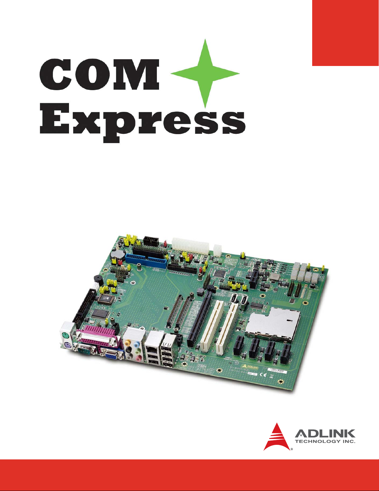
Express-BASE
User’s Manual
Manual Revision: 2.30
Revision Date: July 6, 2011
Part Number: 50-1J012-1030
Page 2
Revision History
Release Date Change
2.00 2006/9/15 Initial Release
2.10 2007/10/19 Updated ETXexpress/Express name changes
2.20 2009/03/05 Updated Engineering Specifications (B2)
2.21 2010/06/11 Updated to D1 PCB version
2.30 2011/07/06 Updated to D2 PCB version: Removed TV-out, extended power
Updated company contact information
(compatible with PICMG COM Express Carrier Design Guide)
connectors; added LVDS panel control header and jumpers, SPI BIOS
socket and Secondary BIOS instructions, ATX 12V 4-pin connector, ATX
power connector info
Express-BASE User’s ManualPage 2
Page 3

Table of Contents
Preface ............................................................................................................................5
1 Introduction...............................................................................................................7
2 Special Features .......................................................................................................8
2.1 Primary LPC based Super I/O...............................................................................................8
2.2 Secondary BIOS ...................................................................................................................8
2.3 Integrated Debug Port with Single Step Execution ...............................................................8
2.4 Onboard Audio......................................................................................................................8
2.5 Information LEDs ..................................................................................................................8
3 Component Location................................................................................................9
4 Function Block Diagram ........................................................................................10
5 Mechanical Dimensions......................................................................................... 11
6 Connectors and Pin-outs.......................................................................................12
6.1 Carrier Board Signals..........................................................................................................12
6.2 Connector and Pinout Compatibility....................................................................................12
6.3 Carrier Board Design ..........................................................................................................12
6.4 COM Express Board-to-Board Connectors.........................................................................13
6.5 PCI Express and PCI Express Graphic (PEG) Slots...........................................................15
6.6 PCI Slots.............................................................................................................................18
6.7 LPC Debug .........................................................................................................................19
6.8 I2C and SMB Bus (for user access)...................................................................................20
6.9 USB and LAN......................................................................................................................22
6.10 Audio...................................................................................................................................23
6.11 VGA, LVDS ......................................................................................................................... 24
6.12 LVDS Jumper Settings........................................................................................................25
6.13 Keyboard & Mouse .............................................................................................................26
6.14 Serial and IrDA Ports ..........................................................................................................26
6.15 Parallel Port ........................................................................................................................27
6.16 Storage: SATA, PATA, FDD, CF..........................................................................................27
6.18 Power Connectors ..............................................................................................................30
Page 3Express-BASE User’s Manual
Page 4

6.19 Power Jumper Settings.......................................................................................................32
6.17 Other Connectors................................................................................................................33
6.20 Other Jumper Settings........................................................................................................35
7 Secondary BIOS......................................................................................................37
7.1 FWH Secondary BIOS - COM.0 Rev. 1.0 ...........................................................................37
7.2 SPI Secondary BIOS - COM.0 Rev. 2.0..............................................................................38
8 Switches, POST, LEDs & Power ............................................................................39
8.1 On/Off and RESET .............................................................................................................39
8.2 POST & Module Type Display.............................................................................................39
8.3 Indicator LEDs ....................................................................................................................40
8.4 Digital I/O LEDs ..................................................................................................................40
8.5 ATX Power Connectors.......................................................................................................41
8.6 AT Power Mode ..................................................................................................................42
Important Safety Instructions .....................................................................................43
Getting Service.............................................................................................................44
Express-BASE User’s ManualPage 4
Page 5

Preface
Copyright 2006-2011 ADLINK Technology, Inc.
This document contains proprietary information protected by copyright. All rights are reserved. No
part of this manual may be reproduced by any mechanical, electronic, or other means in any form
without prior written permission of the manufacturer.
Disclaimer
The information in this document is subject to change without prior notice in order to improve
reliability, design, and function and does not represent a commitment on the part of the manufacturer.
In no event will the manufacturer be liable for direct, indirect, special, incidental, or consequential
damages arising out of the use or inability to use the product or documentation, even if advised
of the possibility of such damages.
Environmental Responsibility
ADLINK is committed to fulfill its social responsibility to global environmental preservation
through compliance with the European Union's Restriction of Hazardous Substances (RoHS)
directive and Waste Electrical and Electronic Equipment (WEEE) directive. Environmental
protection is a top priority for ADLINK. We have enforced measures to ensure that our products,
manufacturing processes, components, and raw materials have as little impact on the
environment as possible. When products are at their end of life, our customers are encouraged to
dispose of them in accordance with the product disposal and/or recovery programs prescribed by
their nation or company.
Trademarks
COM Express™ and PICMG® are registered trademarks of the PCI Industrial Computer
Manufacturers Group.
Product names mentioned herein are used for identification purposes only and may be trademarks and/or registered trademarks of their respective companies.
Page 5Express-BASE User’s Manual
Page 6
Conventions
Take note of the following conventions used throughout this manual to make sure that users
perform certain tasks and instructions properly.
Additional information, aids, and tips that help users perform tasks.
Information to prevent minor physical injury, component damage, data loss,
and/or program corruption when trying to complete a task.
Information to prevent serious physical injury, component damage, data
loss, and/or program corruption when trying to complete a specific task.
Express-BASE User’s ManualPage 6
Page 7

1 Introduction
The COM Express approach of custom carrier combined with off the shelf system cores is an
excellent solution when you need to customize but lack the time or quantity for a complete
redesign. It fits most system integration projects with production volumes from 500 to 10,000 pcs
per year. The COM Express concept has a great many advantages over full custom designs, it
reduces engineering complexity, lowers the threshold for total project quantity and last but not
least brings your product to the market in no time. The average time to design a carrier board is
less than half the time of a full custom OEM board.
Express-BASE is a standard ATX size carrier board. Together with the COM Express module of
your choice and off the shelf add-on cards you can quickly emulate the functionality of your
desired end product for software development and hardware verification.
To build a functional prototype of your target system you will need:
f COM Express module
f Express-BASE carrier board
f PCI Express or PCI add on cards
f PATA / SATA storage or Flash disk solution
The Express-BASE is compatible with Basic and Compact form factor Type 2 pinout COM
Express modules and accommodates up to five PCI Express x1 slots, one PCI Express Graphics
x16 slot, one ExpressCard slot and two PCI slots.
The Express-BASE is based on the PICMG COM Express™ (COM.0 Rev. 2.0) specification and
is compatible with the PICMG COM Express™ Carrier Design Guide (see 6.3 Carrier Board
Design on page 12).
Page 7Express-BASE User’s Manual
Page 8

2 Special Features
2.1 Primary LPC based Super I/O
COM Express modules do not have a Super I/O chip onboard as this is considered legacy.
Therefore, a Super I/O is placed on the carrier board as an optional item. The Express-BASE
uses a Winbond W83627HG-AW that supports FDD, LPT, COM and PS/2 Keyboard and Mouse.
2.2 Secondary BIOS
The Express-BASE using firmware hub (FWH) for COM.0 Rev. 1.0 modules and Serial Peripheral
Interface (SPI) for COM.0 Rev. 2.0 modules. Selection of active BIOS can be made by jumper
setting.
2.3 Integrated Debug Port with Single Step Execution
In addition to a two-digit POST code display, the board also provides a four-digit address display.
By jumper selection the board can be switched into single step BIOS execution mode. Steps are
executed using a manually operated onboard mini switch.
2.4 Onboard Audio
The Express-BASE has a Realtek ALC888 audio codec onboard. Audio I/O is provided by a sixjack connector.
2.5 Information LEDs
General information is obtained through signaling LEDs for HDD, Power and Watchdog status.
Additionally the Express-BASE gives information about module types being plug into the board.
See 8.2 POST & Module Type Display on page 40 and 8.3 Indicator LEDs on page 41.
Express-BASE User’s ManualPage 8
Page 9
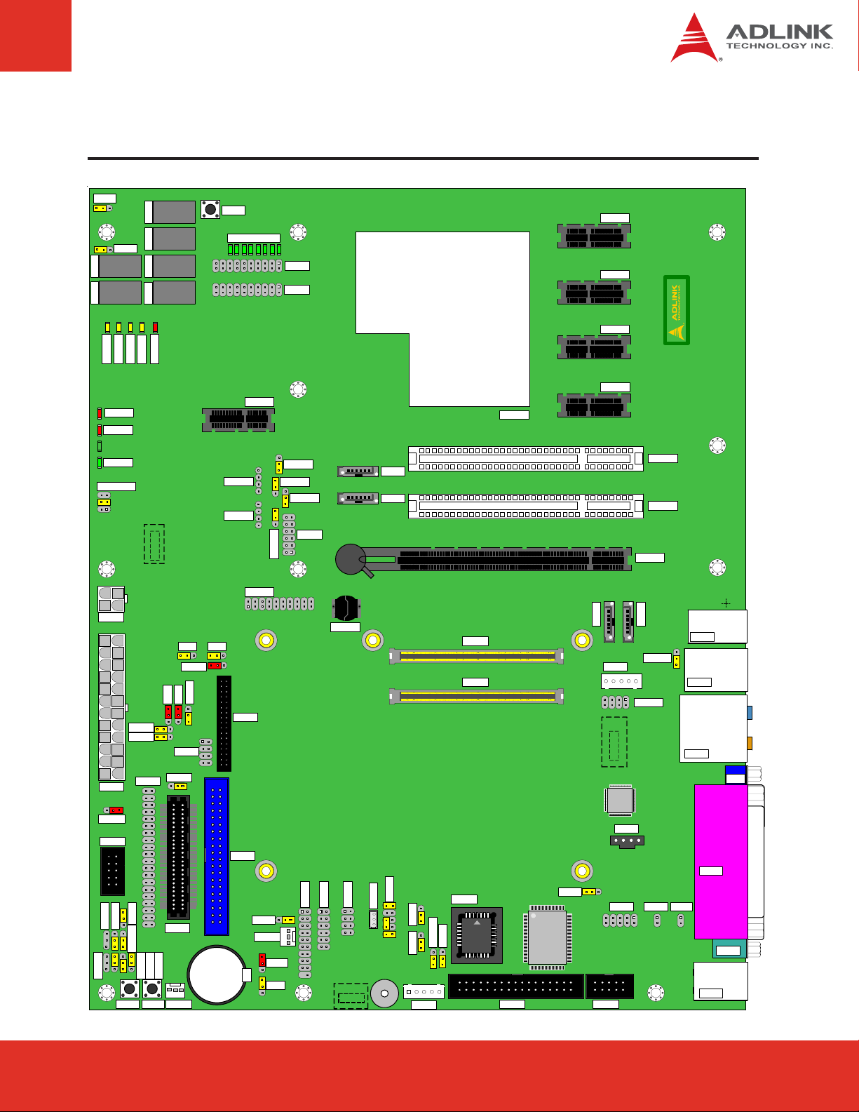
3 Component Location
JP1
LED14LED13
LED15
LED21
LED2
LED20
CNY6
CN42
CN41
JPY10
CNY9
JPY14
JPA6
JPA2
88
LED16
LED17
LED18
JPZ2
JPZ1
CNY4
JP6
JPY13
JPY12
JPA5
SW3 SW1
SW2
LEDX8 – X1
CNY2
CN30
CN31
CNY5
PCIE6
CN32
CNY3
PCIE3
JPY4
JPY5
JPY2
CNY1
JPY3
UZ3
CN11
CN12
CN21
CN20
88 88
LED10 LED11 LED12
LED9
LED19
CN40
JP4
JP3
JPZ3
JP8
JP7
JPY9
CNY8
JPZ4
PCIE5
PCIE4
PCIE2
PCIE1
CN17
CN13
CN16
ALC
CN15
883
PCIA1
PCIE7
CN9
JPY11
CNZ1
PCI2
CN6
CN7
CN2
51-46604-0D20
Express-BASE
CN1
CN35
CN5
CNY7
CN29
CNZ2
JPA4
JPA3
CN37
JPY8
CN33
JPY1
JP5
CN25
CN28
CN26
CN43
CN24
U14
JPZ5
JP2
JPY7 JPY6
CN19 CN18
JPA1
CN8CN10CN14
Winbond
W83627HG-AW
CN3
CN4
Page 9Express-BASE User’s Manual
Page 10
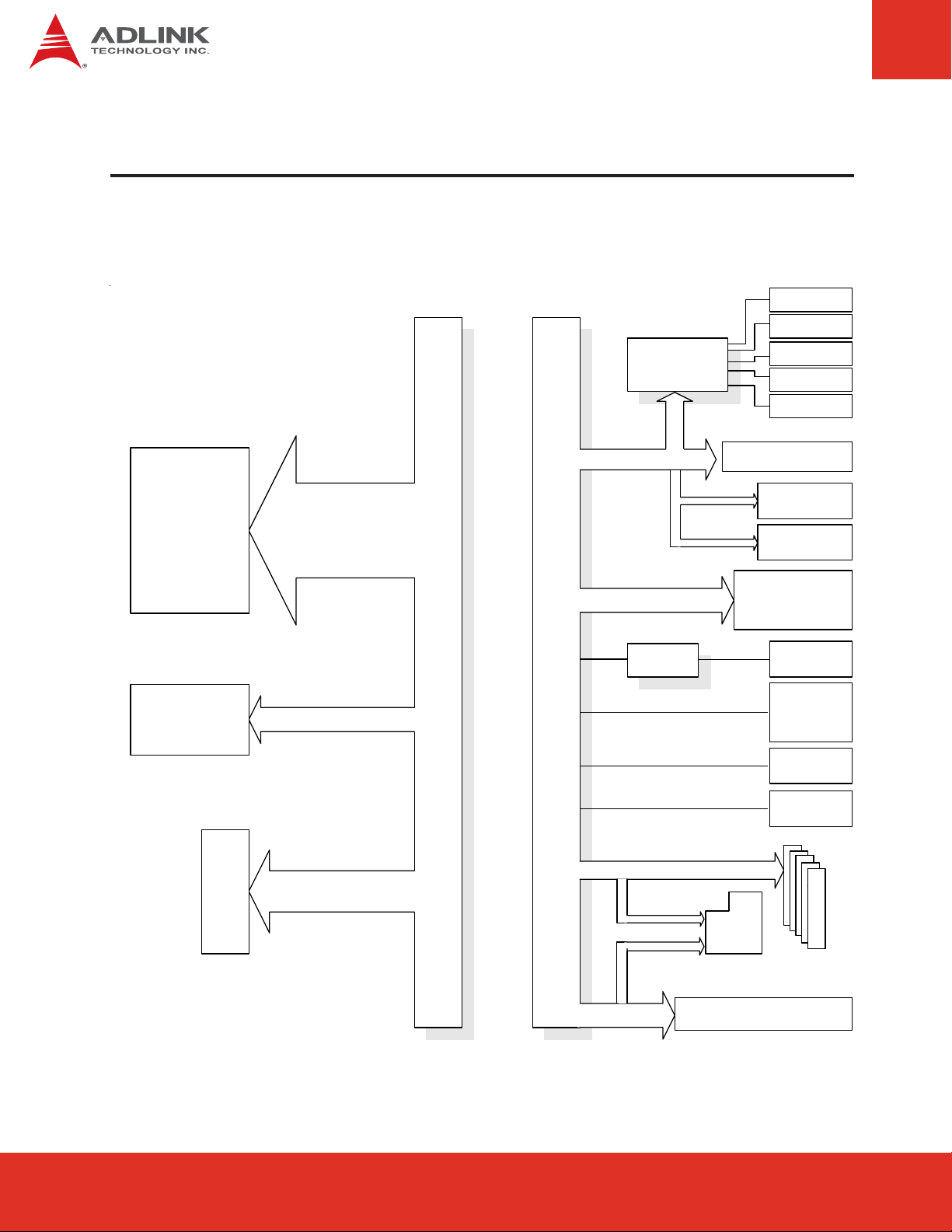
4 Function Block Diagram
W83627HG
Primary
Super I/O
LPT1
COM1
COM2
KB/MS
FDD
PCI Express x16
onboard slot
Onboard IDE
Connector
PCI
2
PCI Express
Graphics x16
PATA
32-bit PCI
CD
AB
LPC
SATA
ALC888
Codec
PCI Express
Debug Header
SATA headers
Express
Card
Secondary
BIOS
POST Code
Display
4 onboard
Audio on
Rear I/O
Gigabit
Ethernet
Rear I/O
CRT VGA
Rear I/O
LVDS
headers
P
P
P
C
P
C
P
C
I
C
I
C
I
E
I
E
I
E
1
E
1
E
1
1
5
USB
6x USB on Rear I/O
1x USB on header
Express-BASE User’s ManualPage 10
Page 11
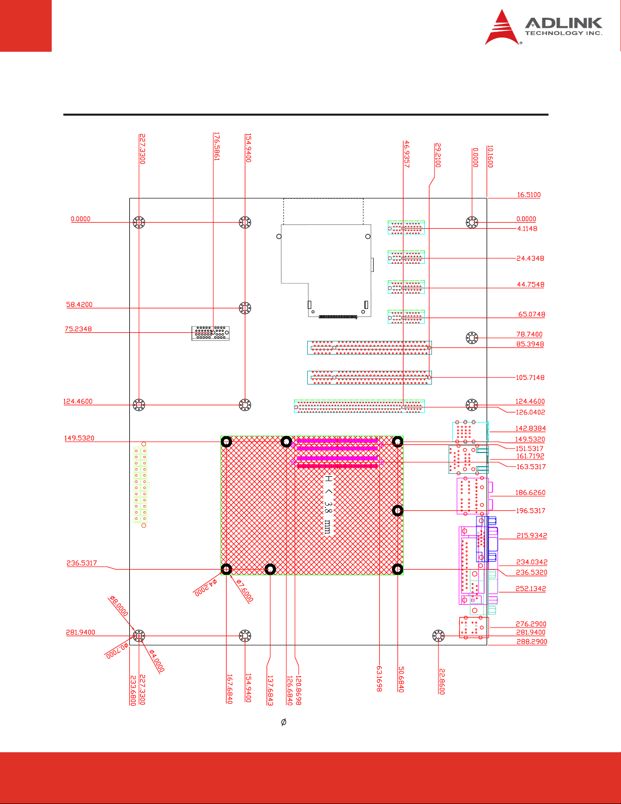
5 Mechanical Dimensions
All tolerances ± 0.05 mm
Other tolerances ± 0.2 mm
Page 11Express-BASE User’s Manual
Page 12
6 Connectors and Pin-outs
6.1 Carrier Board Signals
AB Connector
1 Gigabit Ethernet port
LPC interface
4 Serial ATA channels
High Definition Audio
8 USB 2.0 ports
6 PCI Express Lanes x1
Dual 24-bit LVDS channels
Analog VGA
TV-out ports (SDTV/HDTV)
8 GPIO pins
SMB and I2C bus
+12V primary power input
+5V standby and 3V RTC
C D
A B
6.2 Connector and Pinout Compatibility
Connectors positions and pinouts comply with pinout and signal descriptions in the “PICMG®
COM.0 - COM Express Module Base specification, Revision 2”. This document includes:
description of pinouts, signal descriptions and mechanical characteristics of the COM Express
specification. The Express-BASE is compatible with COM Express modules in Basic and
Compact form factor, Type 2 pinout, COM.0 Rev. 1.0 and Rev. 2.0 .
CD Connector
Parallel ATA, IDE port
alternate definition assigns this to
2 additional Gigabit Ethernet ports
32-bit PCI v2.3 bus
alternate definition assigns this to
10 additional PCI Express x1 lanes
PCI Express x16 for Graphics
these pins can also be assigned to
two SDVO extensions (multiplexed)
+12V primary power input
6.3 Carrier Board Design
The Express-BASE closely follows the PICMG COM Express™
Carrier Design Guide (CDG). Please note that the CDG gives
design advice, and contains unverified reference schematics. The
Express-BASE design and schematics are fully verified, and we
recommend that you follow them as a reference for your carrier
board design.
The CDG and Express-BASE Rev. D2 Schematics and
Mechanical files can be downloaded from the ADLINK
Express-BASE product webpage:
http://www.adlinktech.com/PD/web/PD_detail.php?cKind=&pid=705
Express-BASE User’s ManualPage 12
Page 13
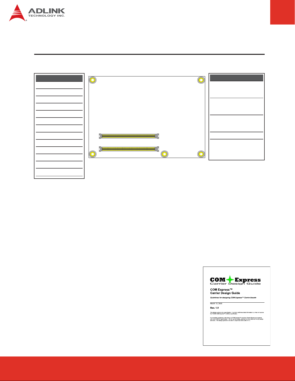
6.4 COM Express Board-to-Board Connectors
R
Signals and Pinout for:
Basic form factor, Type 2.
D1
C1
D110
C D
C110
B1
A1
B110
A110
A B
Row ARow BRow CRow D
Pin No. Pin Na me Pin N o. Pin Name Pi n No. Pin Name Pin No. Pin Name
A1 GND (FIXED) B1 GND (FIXED) C1 GND FIXED) D1 GND FIXED)
A2 GBE0_MDI3- B2 GBE0_ACT# C2 IDE_D7 D2 IDE_D5
A3 GBE0_MDI3+ B3 LPC_FRAME# C3 IDE_D6 D3 IDE_D10
A4 GBE0_LINK100# B4 LPC_AD0 C4 IDE_D3 D4 IDE_D11
A5 GBE0_LINK1000# B5 LPC_AD1 C5 IDE_D15 D5 IDE_D12
A6 GBE0_MDI2- B6 LPC_AD2 C6 IDE_D8 D6 IDE_D4
A7 GBE0_MDI2+ B7 LPC_AD3 C7 IDE_D9 D7 IDE_D0
A8 GBE0_LINK# B8 LPC_DRQ0# C8 IDE_D2 D8 IDE_REQ
A9 GBE0_MDI1- B9 LPC_DRQ1# C9 IDE_D13 D9 IDE_IOW#
A10 GBE0_MDI1+ B10 LPC_CLK C10 IDE_D1 D10 IDE_ACK#
A11 GND (FIXED) B11 GND (FIXED) C11 GND (FIXED) D11 GND (FIXED)
A12 GBE0_MDI0- B12 PWRBTN# C12 IDE_D14 D12 IDE_IRQ
A13 GBE0_MDI0+ B13 SMB_CK C13 IDE_IORDY D13 IDE_A0
A14 GBE0_CTREF B14 SMB_DAT C14 IDE_IOR# D14 IDE_A1
A15 SUS_S3# B15 SMB_ALERT# C15 PCI_PME# D15 IDE_A2
A16 SATA0_TX+ B16 SATA1_TX+ C16 PCI_GNT2# D16 IDE_CS1#
A17 SATA0_TX- B17 SATA1_TX- C17 PCI_REQ2# D17 IDE_CS3#
A18 SUS_S4# B18 SUS_STAT# C18 PCI_GNT1# D18 IDE_RESET#
A19 SATA0_RX+ B19 SATA1_RX+ C19 PCI_REQ1# D19 PCI_GNT3#
A20 SATA0_RX- B20 SATA1_RX- C20 PCI_GNT0# D20 PCI_REQ3#
A21 GND (FIXED) B21 GND (FIXED) C21 GND (FIXED) D21 GND (FIXED)
A22 SATA2_TX+ B22 SATA3_TX+ C22 PCI_REQ0# D22 PCI_AD1
A23 SATA2_TX- B23 SATA3_TX- C23 PCI_RESET# D23 PCI_AD3
A24 SUS_S5# B24 PWR_OK C24 PCI_AD0 D24 PCI_AD5
A25 SATA2_RX+ B25 SATA3_RX+ C25 PCI_AD2 D25 PCI_AD7
A26 SATA2_RX- B26 SATA3_RX- C26 PCI_AD4 D26 PCI_C/BE0#
A27 BATLOW# B27 WDT C27 PCI_AD6 D27 PCI_AD9
A28 (S)ATA_ACT# B28 AC/HDA_SDIN2
A29 AC/HDA_SYNC B29 AC/HDA_SDIN1
A30 AC/HDA_RST# B30 AC/HDA_SDIN0
A31 GND (FIXED) B31 GND (FIXED) C31 GND (FIXED) D31 GND (FIXED)
A32 AC/HDA_BITCLK
A33 AC/HDA_SDOUT
A34 BIOS_DIS0#
A35 THRMTRIP# B35 THRM# C35 PCI_LOCK# D35 PCI_TRDY#
A36 USB6- B36 USB7- C36 PCI_DEVSEL# D36 PCI_FRAME#
A37 USB6+ B37 USB7+ C37 PCI_IRDY# D37 PCI_AD16
A38 USB_6_7_OC# B38 USB_4_5_OC# C38 PCI_C/BE2# D38 PCI_AD18
A39 USB4- B39 USB5- C39 PCI_AD17 D39 PCI_AD20
A40 USB4+ B40 USB5+ C40 PCI_AD19 D40 PCI_AD22
A41 GND (FIXED) B41 GND (FIXED) C41 GND (FIXED) D41 GND (FIXED)
A42 USB2- B42 USB3- C42 PCI_AD21 D42 PCI_AD24
A43 USB2+ B43 USB3+ C43 PCI_AD23 D43 PCI_AD26
A44 USB_2_3_OC# B44 USB_0_1_OC# C44 PCI_C/BE3# D44 PCI_AD28
A45 USB0- B45 USB1- C45 PCI_AD25 D45 PCI_AD30
B32 SPK
B33 I2C_CK C33 PCI_C/BE1# D33 PCI_SERR#
B34 I2C_DAT C34 PCI_PERR# D34 PCI_STOP#
C28 PCI_AD8 D28 PCI_AD11
C29 PCI_AD10 D29 PCI_AD13
C30 PCI_AD12 D30 PCI_AD15
C32 PCI_AD14 D32 PCI_PAR
Pin definitions that are new for COM.0 Rev. 2.0 are highlighted in bold.
Page 13Express-BASE User’s Manual
Page 14
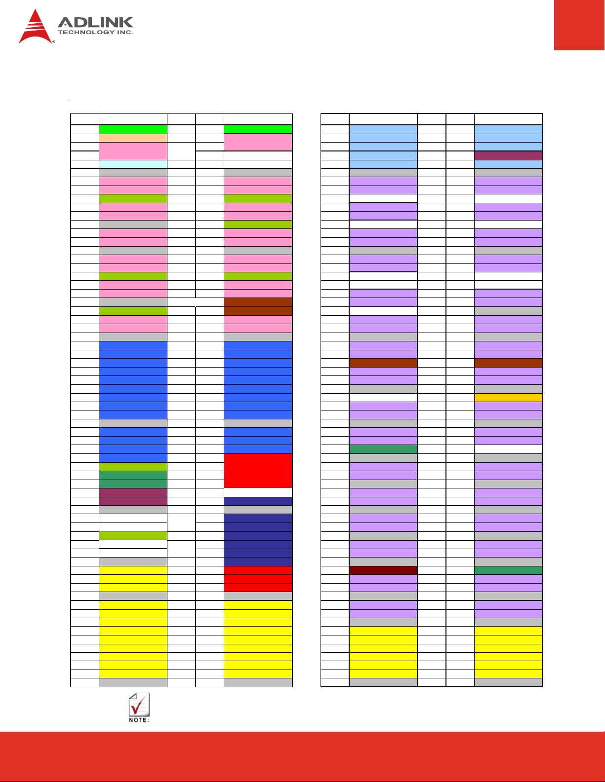
COM Express Board-to-Board Connectors (cont'd):
Row ARow BRow CRow D
Pin No. Pin Name Pin No. Pin Name Pin No. Pin Name Pin No. Pin Name
A46 USB0+ B46 USB1+ C46 PCI_AD27 D46 PCI_IRQC#
A47 VCC_RTC B47 EXCD1_PERST# C47 PCI_AD29 D47 PCI_IRQD#
A48 EXCD0_PERST# B48 EXCD1_CPPE# C48 PCI_AD31 D48 PCI_CLKRUN#
A49 EXCD0_CPPE# B49 SYS_RESET# C49 PCI_IRQA# D49 PCI_M66EN
A50 LPC_SERIRQ B50 CB_RESET# C50 PCI_IRQB# D50 PCI_CLK
A51 GND (FIXED) B51 GND (FIXED) C51 GND (FIXED) D51 GND (FIXED)
A52 PCIE_TX5+ B52 PCIE_RX5+ C52 PEG_RX0+ D52 PEG_TX0+
A53 PCIE_TX5- B53 PCIE_RX5- C53 PEG_RX0- D53 PEG_TX0A54 GPI0 B54 GPO1 C54 TYPE0# D54 PEG_LANE_RV#
A55 PCIE_TX4+ B55 PCIE_RX4+ C55 PEG_RX1+ D55 PEG_TX1+
A56 PCIE_TX4- B56 PCIE_RX4- C56 PEG_RX1- D56 PEG_TX1A57 GND B57 GPO2 C57 TYPE1# D57 TYPE2#
A58 PCIE_TX3+ B58 PCIE_RX3+ C58 PEG_RX2+ D58 PEG_TX2+
A59 PCIE_TX3- B59 PCIE_RX3- C59 PEG_RX2- D59 PEG_TX2A60 GND (FIXED) B60 GND (FIXED) C60 GND (FIXED) D60 GND (FIXED)
A61 PCIE_TX2+ B61 PCIE_RX2+ C61 PEG_RX3+ D61 PEG_TX3+
A62 PCIE_TX2- B62 PCIE_RX2- C62 PEG_RX3- D62 PEG_TX3A63 GPI1 B63 GPO3 C63 RSVD D63 RSVD
A64 PCIE_TX1+ B64 PCIE_RX1+ C64 RSVD D64 RSVD
A65 PCIE_TX1- B65 PCIE_RX1- C65 PEG_RX4+ D65 PEG_TX4+
A66 GND B66 WAKE0# C66 PEG_RX4- D66 PEG_TX4A67 GPI2 B67 WAKE1# C67 RSVD D67 GND
A68 PCIE_TX0+ B68 PCIE_RX0+ C68 PEG_RX5+ D68 PEG_TX5+
A69 PCIE_TX0- B69 PCIE_RX0- C69 PEG_RX5- D69 PEG_TX5A70 GND (FIXED) B70 GND (FIXED) C70 GND (FIXED) D70 GND (FIXED)
A71 LVDS_A0+ B71 LVDS_B0+ C71 PEG_RX6+ D71 PEG_TX6+
A72 LVDS_A0- B72 LVDS_B0- C72 PEG_RX6- D72 PEG_TX6A73 LVDS_A1+ B73 LVDS_B1+ C73 SDVO_DATA D73 SDVO_CLK
A74 LVDS_A1- B74 LVDS_B1- C74 PEG_RX7+ D74 PEG_TX7+
A75 LVDS_A2+ B75 LVDS_B2+ C75 PEG_RX7- D75 PEG_TX7A76 LVDS_A2- B76 LVDS_B2- C76 GND D76 GND
A77 LVDS_VDD_EN B77 LVDS_B3+ C77 RSVD D77 IDE_CBLID#
A78 LVDS_A3+ B78 LVDS_B3- C78 PEG_RX8+ D78 PEG_TX8+
A79 LVDS_A3- B79 LVDS_BKLT_EN C79 PEG_RX8- D79 PEG_TX8A80 GND (FIXED) B80 GND (FIXED) C80 GND (FIXED) D80 GND (FIXED)
A81 LVDS_A_CK+ B81 LVDS_B_CK+ C81 PEG_RX9+ D81 PEG_TX9+
A82 LVDS_A_CK- B82 LVDS_B_CK- C82 PEG_RX9- D82 PEG_TX9A83 LVDS_I2C_CK B83 LVDS_BKLT_CTRL C83 RSVD D83 RSVD
A84 LVDS_I2C_DAT B84 VCC_5V_SBY C84 GND D84 GND
A85 GPI3 B85 VCC_5V_SBY C85PEG_RX10+ D85PEG_TX10+
A86 KBD_RST# B86 VCC_5V_SBY C86PEG_RX10- D86PEG_TX10A87 KBD_A20GATE B87 VCC_5V_SBY C87 GND D87 GND
A88 PCIE_CLK_REF+
A89 PCIE_CLK_REF- B89 VGA_RED C89PEG_RX11- D89PEG_TX11A90 GND (FIXED) B90 GND (FIXED) C90 GND (FIXED) D90 GND (FIXED)
A91 SPI_POWER
A92 SPI_MISO
A93 GPO0 B93 VGA_HSYNC C93 GND D93 GND
A94 SPI_CLK
A95 SPI_MOSI
A96 GND B96 VGA_I2C_DAT C96 GND D96 GND
A97 TYPE10# B97 SPI_CS#
A98 RSVD B98 RSVD
A99 RSVD B99 RSVD
A100 GND (FIXED) B100 GND (FIXED) C100 GND (FIXED) D100 GND (FIXED)
A101 RSVD B101 RSVD
A102 RSVD B102 RSVD
A103 RSVD B103 RSVD
A104 VCC_12V B104 VCC_12V C104 VCC_12V D104 VCC_12V
A105 VCC_12V B105 VCC_12V C105 VCC_12V D105 VCC_12V
A106 VCC_12V B106 VCC_12V C106 VCC_12V D106 VCC_12V
A107 VCC_12V B107 VCC_12V C107 VCC_12V D107 VCC_12V
A108 VCC_12V B108 VCC_12V C108 VCC_12V D108 VCC_12V
A109 VCC_12V B109 VCC_12V C109 VCC_12V D109 VCC_12V
A110 GND (FIXED) B110 GND (FIXED) C110 GND (FIXED) D110 GND (FIXED)
B88 BIOS_DIS1#
B91 VGA_GRN C91PEG_RX12+ D91PEG_TX12+
B92 VGA_BLU C92PEG_RX12- D92PEG_TX12-
B94 VGA_VSYNC C94PEG_RX13+ D94PEG_TX13+
B95 VGA_I2C_CK C95PEG_RX13- D95PEG_TX13-
C88PEG_RX11+ D88PEG_TX11+
C97 RSVD D97 PEG_ENABLE#
C98PEG_RX14+ D98PEG_TX14+
C99PEG_RX14- D99PEG_TX14-
C101 PEG_RX15+ D101 PEG_TX15+
C102 PEG_RX15- D102 PEG_TX15C103 GND D103 GND
Pin definitions that are new for COM.0 Rev. 2.0 are highlighted in bold.
Express-BASE User’s ManualPage 14
Page 15

6.5 PCI Express and PCI Express Graphic (PEG) Slots
PCI Express x1:
PCIE1
PCIE2
PCIE4
PCIE5
PCIE6
B1
B11
B12
B18
A1
A11
A12
A18
Pin Signal Pin Signal
B1 + 12V A1 NC
B2 + 12V A2 + 12V
B3 NC A3 + 12V
B4 GND A4 GND
B5 SMB_CK A5 TCK
B6 SMB_DAT A6 TDI
B7 GND A7 NC
B8 + 3.3V A8 TMS
B9 TRST# A9 + 3.3V
B10 +3.3VSB A10 + 3.3V
B11 WAKE# A11 PERST#
B12 NC A12 GND
B13 GND A13 REFCLK+
B14 PETp0 A14 REFCLKB15 PETn0 A15 GND
B16 GND A16 PERp0
B17 NC A17 PERn0
B18 GND A18 GND
CN44: ExpressCard (PCIE3, USB7)
Pin Signal Pin Signal
1 GND 14 +3.3V
2 USBD- 15 +3.3V
3 USBD+ 16 CLKREQ#
4 CPUSB# 17 CPPE#
5 RESERVED 18 REFCLK6 RESERVED 19 REFCLK+
7 SMB_CK 20 GND
8 SMB_DAT 21 PERn0
9 +1.5V 22 PERp0
10 +1.5V 23 GND
11 WAKE# 24 PETn0
12 +3.3VSB 25 PETp0
13 PERST# 26 GND
Page 15Express-BASE User’s Manual
Page 16

A1A11A12A82
B1B11B12B82
PCIE7: PCI Express x16 mode
See the JP6 jumper description for PCI Express x16 mode and SDVO mode settings on p. 35.
Pin Signal Pin Signal
B1 + 12V A1 NC
B2 + 12V A2 + 12V
B3 NC A3 + 12V
B4 GND A4 GND
B5 SMB_CK A5 TCK
B6 SMB_DAT A6 TDI
B7 GND A7 NC
B8 + 3.3V A8 TMS
B9 TRST# A9 + 3.3V
B10 +3.3VSB A10 + 3.3V
B11 WAKE# A11 PERST#
B12 NC A12 GND
B13 GND A13 REFCLK+
B14 PETp0 A14 REFCLKB15 PETn0 A15 GND
B16 GND A16 PERp0
B17 RSVD A17 PERn0
B18 GND A18 GND
B19 PETp1 A19 NC
B20 PETn1 A20 GND
B21 GND A21 PERp1
B22 GND A22 PERn1
B23 PETp2 A23 GND
B24 PETn2 A24 GND
B25 GND A25 PERp2
B26 GND A26 PERn2
B27 PETp3 A27 GND
B28 PETn3 A28 GND
B29 GND A29 PERp3
B30 NC A30 PERn3
B31 RSVD A31 GND
B32 GND A32 NC
B33 PETp4 A33 NC
B34 PETn4 A34 GND
B35 GND A35 PERp4
B36 GND A36 PERn4
B37 PETp5 A37 GND
B38 PETn5 A38 GND
B39 GND A39 PERp5
B40 GND A40 PERn5
B41 PETp6 A41 GND
Pin Signal Pin Signal
B42 PETn6 A42 GND
B43 GND A43 PERp6
B44 GND A44 PERn6
B45 PETp7 A45 GND
B46 PETn7 A46 GND
B47 GND A47 PERp7
B48 NC A48 PERn7
B49 GND A49 GND
B50 PETp8 A50 NC
B51 PETn8 A51 GND
B52 GND A52 PERp8
B53 GND A53 PERn8
B54 PETp9 A54 GND
B55 PETn9 A55 GND
B56 GND A56 PERp9
B57 GND A57 PERn9
B58 PETp10 A58 GND
B59 PETn10 A59 GND
B60 GND A60 PERp10
B61 GND A61 PERn10
B62 PETp11 A62 GND
B63 PETn11 A63 GND
B64 GND A64 PERp11
B65 GND A65 PERn11
B66 PETp12 A66 GND
B67 PETn12 A67 GND
B68 GND A68 PERp12
B69 GND A69 PERn12
B70 PETp13 A70 GND
B71 PETn13 A71 GND
B72 GND A72 PERp13
B73 GND A73 PERn13
B74 PETp14 A74 GND
B75 PETn14 A75 GND
B76 GND A76 PERp14
B77 GND A77 PERn14
B78 PETp15 A78 GND
B79 PETn15 A79 GND
B80 GND A80 PERp15
B81 NC A81 PERn15
B82 NC A82 GND
Express-BASE User’s ManualPage 16
Page 17

PCIE7: SDVO mode
A1A11A12A82
B1B11B12B82
See the JP6 jumper description for PCI Express x16 mode and SDVO mode settings on p. 35.
Pin Signal Pin Signal
B1 + 12V A1 NC
B2 + 12V A2 + 12V
B3 NC A3 + 12V
B4 GND A4 GND
B5 SMB_CK A5 TCK
B6 SMB_DAT A6 TDI
B7 GND A7 NC
B8 + 3.3V A8 TMS
B9 TRST# A9 + 3.3V
B10 +3.3VSB A10 + 3.3V
B11 WAKE# A11 PERST#
B12 NC A12 GND
B13 GND A13 REFCLK+
B14 SDVOB_RED+ A14 REFCLKB15 SDVOB_RED- A15 GND
B16 GND A16 SDVO_TVCLKIN+
B17 SDVO_CLK A17 SDVO_TVCLKINB18 GND A18 GND
B19 SDVOB_GRN+ A19 NC
B20 SDVOB_GRN- A20 GND
B21 GND A21 SDVOB_INT+
B22 GND A22 SDVOB_INTB23 SDVOB_BLU+ A23 GND
B24 SDVOB_BLU- A24 GND
B25 GND A25 SDVO_FLDSTALL+
B26 GND A26 SDVO_FLDSTALLB27 SDVOB_CK+ A27 GND
B28 SDVOB_CK- A28 GND
B29 GND A29 RSVD
B30 NC A30 RSVD
B31 SDVO_DAT A31 GND
B32 GND A32 NC
B33 SDVOC_RED+ A33 NC
B34 SDVOC_RED- A34 GND
B35 GND A35 RSVD
B36 GND A36 RSVD
B37 SDVOC_GRN+ A37 GND
B38 SDVOC_GRN- A38 GND
B39 GND A39 RSVD
B40 GND A40 RSVD
B41 SDVOC_BLU+ A41 GND
Pin Signal Pin Signal
B42 SDVOC_BLU- A42 GND
B43 GND A43 RSVD
B44 GND A44 RSVD
B45 SDVOC_CK+ A45 GND
B46 SDVOC_CK- A46 GND
B47 GND A47 RSVD
B48 NC A48 RSVD
B49 GND A49 GND
B50 RSVD A50 NC
B51 RSVD A51 GND
B52 GND A52 RSVD
B53 GND A53 RSVD
B54 RSVD A54 GND
B55 RSVD A55 GND
B56 GND A56 RSVD
B57 GND A57 RSVD
B58 RSVD A58 GND
B59 RSVD A59 GND
B60 GND A60 RSVD
B61 GND A61 RSVD
B62 RSVD A62 GND
B63 RSVD A63 GND
B64 GND A64 RSVD
B65 GND A65 RSVD
B66 RSVD A66 GND
B67 RSVD A67 GND
B68 GND A68 RSVD
B69 GND A69 RSVD
B70 RSVD A70 GND
B71 RSVD A71 GND
B72 GND A72 RSVD
B73 GND A73 RSVD
B74 RSVD A74 GND
B75 RSVD A75 GND
B76 GND A76 RSVD
B77 GND A77 RSVD
B78 RSVD A78 GND
B79 RSVD A79 GND
B80 GND A80 RSVD
B81 NC A81 RSVD
B82 NC A82 GND
Page 17Express-BASE User’s Manual
Page 18

6.6 PCI Slots
PCI interrupts
OnboardDevice Pin INTA# Pin INTB# Pin INTC# Pin INTD# IDSEL
PCIA1 X1_INTA# X1_INTB# X1_INTC# X1_INTD# AD20
PCI2 X1_INTB# X1_INTC# X1_INTD# X1_INTA# AD21
A1
PCIA1, PCI2: 32-bit PCI slot
B1
A Signal B Signal
1 TRST_L 1 -12V
2 +12V 2 TCK
3 TMS 3 Ground
4 TDI 4 TDO
5 +5V 5 +5V
6 INTA_L 6 +5V
7 INTC_L 7 INTB_L
8 +5V 8 INTD_L
9 Reserved 9 PRSNT1_L
10 +5V 10 Reserved
11 Reserved 11 PRSNT2_L
12 Ground 12 Ground
13 Ground 13 Ground
14 Reserved 14 Reserved
15 RST_L 15 Ground
16 +5V 16 CLK
17 GNT_L 17 Ground
18 Ground 18 REQ_L
19 Reserved 19 +5V
20 AD[30] 20 AD[31]
21 +3.3V 21 AD[29]
22 AD[28] 22 Ground
23 AD[26] 23 AD[27]
24 Ground 24 AD[25]
25 AD[24] 25 +3.3V
26 IDSEL 26 C/BE[3]_L
27 +3.3V 27 AD[23]
28 AD[22] 28 Ground
29 AD[20] 29 AD[21]
30 Ground 30 AD[19]
31 AD[18] 31 +3.3V
A62
B62
A Signal B Signal
32 AD[16] 32 AD[17]
33 +3.3V 33 C/BE[2]_L
34 FRAME_L 34 Ground
35 Ground 35 IRDY_L
36 TRDY_L 36 +3.3V
37 Ground 37 DEVSEL_L
38 STOP_L 38 Ground
39 +3.3V 39 LOCK_L
40 Reserved 40 PERR_L
41 Reserved 41 +3.3V
42 Ground 42 SERR_L
43 PAR 43 +3.3V
44 AD[15] 44 C/BE[1]_L
45 +3.3V 45 AD[14]
46 AD[13] 46 Ground
47 AD[11] 47 AD[12]
48 Ground 48 AD[10]
49 AD[09] 49 Ground
50 KEYWAY 50 KEYWAY
51 KEYWAY 51 KEYWAY
52 C/BE[0]_L 52 AD[08]
53 +3.3V 53 AD[07]
54 AD[06] 54 +3.3V
55 AD[04] 55 AD[05]
56 Ground 56 AD[03]
57 AD[02] 57 Ground
58 AD[00] 58 AD[01]
59 +5V 59 +5V
60 REQ64_L 60 ACK64_L
61 +5V 61 +5V
62 +5V 62 +5V
Express-BASE User’s ManualPage 18
Page 19

6.7 LPC Debug
CN32: LPC Debug header
12
19 20
CNY1: LPC Test Connector
(compatible with ADLINK
LPC Debug Card)
Pin Signal Pin Signal
1 LPC_CLK 2 GND
3 LPC_FRAME# 4 KEY
5 LPC_RST# 6 + 5V
7 LPC_AD3 8 LPC_AD2
9 + 3.3V 10 L_AD1
11 LPC_AD0 12 GND
13 SMB_CK 14 SMB_DAT
15 SPD_A1 (See JP3) 16 SPD_A0 (See JP4)
17 GND 18 LPC_SERIRQ
19 KBRST# 20 A20GATE#
Pin Signal Pin Signal
1 LPC_DRQ0# 2 LPC_AD0
3 LPC_DRQ1# 4 LPC_AD1
5 LPC_SERIRQ 6 LPC_AD2
7 LPC_FRAME# 8 LPC_AD3
9 LPC_RST# 10 GND
11 LPC_CLK 12 GND
External LPC EEPROM Address Selection
JP3 & JP4 configure the address of the external EEPROM connected to the LPC Debug header (CN32)
JP3: EEPROM Address A0 Selection
1
2
3
JP4: EEPROM Address A1 Selection
1
2
3
NOTE: <<<< indicates default setting
Jumper Status
1-2 High "1" <<<<
2-3 Low "0"
Jumper Status
1-2 High "1" <<<<
2-3 Low "0"
Page 19Express-BASE User’s Manual
Page 20

6.8 I2C and SMB Bus
(for user access)
CN31: I2C Bus
1
CN30: SMB Bus
1
Pin Signal
1 +5V
2 I2C_DAT
3 I2C_CK
4 GND
Pin Signal
1 +5V
2 SMB_DAT
3 SMB_CK
4 GND
I2C/SMBus Buffers
These buffers settings are for isolation of the I2C and SMBus - test feature only.
ON: I2C/SMBus passes through LTC4300A-2 Buffer
OFF: Bypass Buffer
JPY2: I2C BUFFER (data)
1
2
3
Jumper Status
1-2 ON
2-3 OFF <<<<
JPY3: I2C BUFFER (clock)
JPY4: SMBus BUFFER (data)
JPY5: SMBus BUFFER (clock)
1
2
3
1
2
3
1
2
3
Jumper Status
1-2 ON
2-3 OFF <<<<
Jumper Status
1-2 ON
2-3 OFF <<<<
Jumper Status
1-2 ON
2-3 OFF <<<<
NOTE: <<<< indicates default setting
Express-BASE User’s ManualPage 20
Page 21

I2C EEPROM Address Selection
JPY12 to JPY14 configure the address of the A0, A1 and A2 bits of the I2C EEPROM
JPY12: I2C EEPROM A0
JPY13: I2C EEPROM A1
JPY14: I2C EEPROM A2
1
2
3
1
2
3
1
2
3
Jumper Status
1-2 A0_HIGH "1"
2-3 A0_LOW "0" <<<<
Jumper Status
1-2 A1_HIGH "1"
2-3 A1_LOW "0" <<<<
Jumper Status
1-2 A2_HIGH "1"
2-3 A2_LOW "0" <<<<
NOTE: <<<< indicates default setting
Page 21Express-BASE User’s Manual
Page 22

6.9 USB and LAN
CN6: USB x4 Connector
CN7: RJ-45 Gbe LAN
+ USB
Pin Signal
1 +5V
2 USB3 USB+
4 Ground
Pin Signal
1 MDI[0]+
2 MDI[0]3 MDI[1]+
4 MDI[1]5 MDI[2]+
6 MDI[2]7 MDI[3]+
8 MDI[3]-
CN13: USB Header
1
Pin Signal
1 +5V
2 USB3 USB+
4 Ground
Pin Signal
1 +5V
2 USB3 USB+
4 Ground
Express-BASE User’s ManualPage 22
Page 23

6.10 Audio
CN2: Six-in-One
Audio Phone Jack
CN14: Audio Pin Header
9
1
CN8: SPDIF Input Header
1
Color Signal
BLUE Line-In
GREEN Line-Out
PINK MIC-In
ORANGE Center/Subwoofer
BLACK Rear Speaker Out
GRAY Side Speaker Out
Pin Signal Pin Signal
1 MIC-In-L 2 AGND
3 MIC-In-R 4 ACZ Detect
5 Line-In-R 6 MIC-In Detect
7 Front I/O Sense 8 Key
9 Line-In-L 10 Line-In Detect
Pin Signal Pin Signal
1 SPDIF-In 2 GND
CN10: SPDIF Output Header
1
Pin Signal Pin Signal
1 SPDIF-Out 2 GND
CN15: CD Audio-out Connector
CNZ1: AC’97 Pin Header
1
7
Pin Signal Pin Signal
1 GND 2 AC_SYNC
3 AC_SDOUT 4 AC_RST#
5 AC_BITCLK 6 GND
7 AC_SDIN0 8 NC
Pin Signal
1 LINR
2 AGND
1
3 AGND
4 LINL
Page 23Express-BASE User’s Manual
Page 24

6.11 VGA, LVDS
CN1: VGA
CNY5: LVDS Flat Panel Connector
Pin Signal Pin Signal
1 Red 2 Green
3 Blue 4 NC
5 GND 6 GND
7 GND 8 GND
9 NC 10 GND
11 DDC Power 12 DDC2B Data
13 HSYNC 14 Vsync
15 DDC2B clock
Pin Signal Pin Signal
1 LVDS_I2C_DAT 2 LVDS_I2C_CK
3 N.C 4 N.C
5 GND 6 LVDS_A07 LVDS_A0+ 8 LVDS_VDD_EN
9 LVDS_A1- 10 LVDS_A1+
11 LVDS_BKLT_EN 12 LVDS_A2+
13 LVDS_A2- 14 N.C
15 LVDS_A_CK- 16 LVDS_A_CK+
17 N.C 18 LVDS_A3+
19 LVDS_A3- 20 GND
21 LVDS_B0- 22 LVDS_B0+
23 GND 24 LVDS_B125 LVDS_B1+ 26 GND
27 LVDS_B2- 28 LVDS_B2+
29 GND 30 LVDS_B_CK+
31 LVDS_B_CK- 32 N.C
33 LVDS_B3+ 34 LVDS_B3-
CNY8: Backlight Control
See 6.12 LVDS Jumper Settings for Panel Power Voltage (JP8), Backlight Power Voltage
(JP7) and other LVDS jumper settings.
To avoid damage to the display panel, be sure to set the Panel Power Voltage (JP8) and
Backlight Power Voltage (JP7) to the correct values for your display.
12
Pin Signal Pin Signal
1 GND 2 Panel PWR
3 Backlight CTRL 4 GND
5 Backlight Enable 6 GND
7 NC 8 Backlight PWR
Express-BASE User’s ManualPage 24
Page 25

6.12 LVDS Jumper Settings
JP7: Backlight Power Voltage
Selects the Backlight Power voltage on CNY8
Backlight Control pin header (pin 8).
JP8: Panel Power Voltage
Selects the Panel Power voltage on CNY8
Backlight Control pin header (pin 2).
JPZ1: Brightness Control
Sets the Panel Brightness Control (CNY8 pin 3:
Backlight CTRL) to Voltage Level or PWM .
When set to Voltage Level, the Backlight CTRL
signal can be varied from 0~5V in 0.5V
increments.
JPZ2: Brightness PWM Source
Sets the Panel Brightness PWM Source
to GPU or LVDS I2C. When Brightness PWM
Source is set to LVDS I2C, the user will be able
to use the AIDI Library AidiVgaSetBacklight
command to control the PWM pulse to the panel
backlight.
1
2
3
1
2
3
1
2
3
1
2
3
Jumper Status
1-2 + 12V
2-3 + 5V <<<<
Jumper Status
1-2 + 3.3V <<<<
2-3 + 5V
Jumper Status
1-2 Voltage Level
2-3 PWM <<<<
Jumper Status
1-2 GPU
2-3 LVDS I2C <<<<
JPY9: Backlight Enable Signal Type
Sets the Backlight Enable Signal to "Normal"
1
2
3
or "Inverse" type.
NOTE: <<<< indicates default setting
Jumper Status
1-2 Inverse
2-3 Normal <<<<
Page 25Express-BASE User’s Manual
Page 26

6.13 Keyboard & Mouse
CN4: Mouse (top)
Keyboard (bottom)
6.14 Serial and IrDA Ports
CN3: COM1 (DB9)
65
4
21
65
4
21
3
3
Pin Signal Pin Signal
6 DSR 1 DCD#
7 RTS# 2 RXD
8 CTS# 3 TXD
9 RI# 4 DTR#
Pin Signal
1 MSDAT
2NC
3 GND
4 KB5V
5 MSCLK
6NC
Pin Signal
1 KBDAT
2NC
3 GND
4 KB5V
5 KBCLK
6NC
5 GND
CN18: COM2 (header)
CN24: IrDA Connector
Pin Signal Pin Signal
5
1
1
1 DCD# 6 DSR
2 RXD 7 RTS#
3 TXD 8 CTS#
4 DTR# 9 RI#
5 GND 10 NC
Pin Signal
1 +5V
2 No connect
3 IrRXD
4 Ground
5 IrTXD
Express-BASE User’s ManualPage 26
Page 27

6.15 Parallel Port
CN5: DB25
Pin Signal Pin Signal
1 STROBE# 14 AUTOFD#
2 DATA0 15 ERROR#
3 DATA1 16 INIT#
4 DATA2 17 SELIN#
5 DATA3 18 GND
6 DATA4 19 GND
7 DATA5 20 GND
8 DATA6 21 GND
9 DATA7 22 GND
10 ACK# 23 GND
11 BUSY 24 GND
12 PAPER EMPTY 25 GND
13 SEL 26 N/C
6.16 Storage: SATA, PATA, FDD, CF
CN9/11/12/17: SATA
1 7
Pin Signal Pin Signal
1 GND 2 Tx+
3 Tx- 4 GND
5 Rx- 6 Rx+
7 GND
Page 27Express-BASE User’s Manual
Page 28
CN19: FDD Connector
1 2
33 34
Pin Signal Pin Signal
1 Ground 2 Drive density selection
0
3 Ground 4 N.C.
5 N.C. 6 Drive density selection
1
7 Ground 8 Index
9 Ground 10 Motor enable 0 (1)
11 Ground 12 Drive select 1
13 Ground 14 Drive select 0 (1)
15 Ground 16 Motor enable 1
17 Ground 18 Direction
19 Ground 20 Step
21 Ground 22 Write data
23 Ground 24 Write gate
25 Ground 26 Track 00
27 Ground 28 Write protect
29 Ground 30 Read data
31 Ground 32 Side 1 select
33 Ground 34 Diskette change
CN35: IDE Connector
1 2
39 40
Pin Signal Pin Signal
1 Reset IDE 2 GND
3 IDE Data 7 4 IDE Data 8
5 IDE Data 6 6 IDE Data 9
7 IDE Data 5 8 IDE Data 10
9 IDE Data 4 10 IDE Data 11
11 IDE Data 3 12 IDE Data 12
13 IDE Data 2 14 IDE Data 13
15 IDE Data 1 16 IDE Data 14
17 IDE Data 0 18 IDE Data 15
19 Ground 20 KEY
21 DREQ0 22 GND
23 IDEIOW# 24 GND
25 IDEIOR# 26 GND
27 IDEIORDY 28 CBSEL
29 DACK0# 30 GND
31 IDEIRQ14 32 NC
33 IDE Address 1 34 PDIAG#
35 IDE Address 0 36 IDE Address 2
37 IDE Chip select 1# 38 IDE Chip select 3#
39 IDE activity 40 GND
Express-BASE User’s ManualPage 28
Page 29

CNZ2: CF Socket
Pin Signal Pin Signal
1 GND 2 IDE_D3
3 IDE_D4 4 IDE_D5
5 IDE_D6 6 IDE_D7
7 IDE_CS1J 8 GND
9 GND 10 GND
11 GND 12 GND
13 5VCC 14 GND
15 GND 16 GND
17 GND 18 IDE_A2
19 IDE_A1 20 IDE_A0
21 IDE_D0 22 IDE_D1
23 IDE_D2 24 IOIS16J
25 GND 26 GND
27 IDE_D11 28 IDE_D12
1
29 IDE_D13 30 IDE_D14
31 IDE_D15 32 IDE_CS3J
33 GND 34 IDE_IORJ
35 IDE_IOWJ 36 CFWE
37 IDE_IRQ 38 5VCC
39 CFSCSEL 40 NC
41 PLTRSTJ 42 IDE_IORDY
43 IDE_REQJ 44 IDE_ACKJ
45 IDE_ACTJ 46 IDE_66DECT
47 IDE_D8 48 IDE_D9
49 IDE_D10 50 GND
JPZ4: CF Master/Slave Setting
The default setting is CF slot (CNZ2) Master
and IDE Slave (CN35).
1
2
3
Jumper Status
1-2 CF Master <<<<
2-3 CF Slave
Page 29Express-BASE User’s Manual
Page 30

6.18 Power Connectors
CN33/37: 12 V Fan Power
321
Pin Signal
1 FAN Tach output
2 12 V
3 GND
CN41: ATX 24-pin Power Connector
+3.3 V
Connect the ATX 24-pin (or 20-pin) connector
to supply power to the Express-BASE carrier.
-12 V
COM
PWR_ON
COM
COM
COM
-5 V
+5 V
+5 V
+5 V
COM
+3.3 V
13
14
15
16
17
18
19
20
21
22
23
24
1
2
3
4
5
6
7
8
9
10
11
12
+3.3 V
Ground
+5 V
Ground
+5 V
Ground
PWR_GOOD
+5 V
SB
+12 V
+12 V
+3.3 V
CN42: ATX 12V 4-pin Connector
Connect the ATX 12V 4-pin connector to
supply power to the COM Express module.
All 12V power for the COM Express module is provided by the ATX 12V 4-pin connector.
The system will not power up if CN42 is not connected to the power supply.
To avoid damage to the carrier board and installed components, be sure to connect the
ATX power supply to the correctly connectors. See 8.5 ATX Power Connectors on page 42
for detailed information.
Pin Signal
24
1
3
1 GND
2 GND
3 +12V
4 +12V
Express-BASE User’s ManualPage 30
Page 31

CN43: 5 Volt FAN Power
321
CNY9: Smart Battery
Pin Signal
15 V
2 GND
3 FAN Tach output
Connects to Smart Battery
module
Pin Signal Pin Signal
1 I2C_CK 6 SUS_S45#
2 I2C_DAT 7 +12V
3 PWRBTN# 8 +5VSB
4 BATLOW# 9 SUS_STAT#
5 PS_ON# 10 GND
Page 31Express-BASE User’s Manual
Page 32

6.19 Power Jumper Settings
CNY6: PWR_OK Config
CNY7: Power Up Config
*The Super I/O detects a power button event using the 'PSIN' pin. When a power button event occurs, the powerup logic of the Super I/O sets 'PSOUT#' low and asserts 'PWRBTN#' of the module's chipset. The Super I/O also
sets the 'PWRCTL#' pin to low, which asserts the 'PS_ON#' signal and switches on the ATX power supply.
JPY1: AT/ATX MODE
In AT mode, JPY1 shorts PS_ON# to ground
Jumper Status
1-2 Add 3.3V Pullup with 10K to signal PWR_OK
3-4 Connect PWRGOOD of ATX power supply <<<<
5-6 Connect PWRGOOD of onboard DCDC regulator
Jumper Status
101
1-10
5-6 Power-up by module <<<<
8-9
2-9
3-8 Power-up by Super I/O*
5
6
4-7
1
2
3
Jumper Status
1-2 A TX Mode <<<<
2-3 A T Mode
directly to force power on.
JPY10: PS_ON# Signal Source
All ADLINK modules support S3 mode and
1
2
3
Jumper Status
1-2 SUS_S3# <<<<
2-3 SUS_S5#
consecutive power down of ATX power supply.
For modules that connect the S3 signal, PS_ON#
should always be set to SUS_S3# as source (even when S3 mode is disabled in the BIOS). For
modules that do not bring out the S3 signal, PS_ON# should be set to SUS_S5# as source.
JPZ3: AT Power 5V Setting
With an AT power supply is connected to
1
2
3
Jumper Status
1-2 AT without P5V <<<<
2-3 AT with P5V
the Express-BASE, JPZ3 can be used to
provide 5VSB to the COM module from
the carrier board.
NOTE: <<<< indicates default setting
Express-BASE User’s ManualPage 32
Page 33

6.17 Other Connectors
CN25: GPIO Header
GPIOs of CN25 come from
the COM Express module.
CN29: Miscellaneous
Connector
12
78
1 11
10 20
Pin Signal Pin Signal
1 GPI0 2 GPO0
3 GPI1 4 GPO1
5 GPI2 6 GPO2
7 GPI3 8 GPO3
Pin Signal Pin Signal
1 Power LED 11 Speaker
2 Power LED 12 Speaker
3 Power LED 13 Speaker
4 Keyboard Lock 14 Speaker
5 Keyboard Lock 15 RESET
6 NC 16 RESET
7 NC 17 HDD LED
8 NC 18 HDD LED
9 NC 19 Power Button
10 NC 20 Power Button
CNY2-3: Digital I/O
The Express-Base provides
GPIO expansion for I²C
applications via a Phillips
PCA955 with 16-bit I²C
I/O port and interrupt.
Pin Signal Pin Signal
1 I/O 0 11 GND
2 I/O 1 12 GND
3 I/O 2 13 GND
4 I/O 3 14 GND
5 I/O 4 15 GND
6 I/O 5 16 GND
7 I/O 6 17 GND
8 I/O 7 18 GND
9 INT# 19 BATLOW#
10 3V3 20 +3.3V
Page 33Express-BASE User’s Manual
Page 34

CNY4: Feature Connector
12
39 40
Pin Signal Pin Signal
1 +5V 2 +5VSB
3 +5V 4 Hard Disk Activity
5 I2C_DAT 6 SMBCLK_SB
7 I2C_CK 8 SMBDATA_SB
9 Internal use 10 GPO0
11 Internal use 12 GPO1
13 PS_ON# 14 GPO2
15 SUS_S3# 16 GPO3
17 GND 18 GND
19 THRMTRIP# 20 SMBALRT#
21 GPI1 22 SUS_S4#
23 SUS_STAT# 24 GPI0
25 GPI2 26 SUS_S5#
27 WDTRIG 28 THRM#
29 GPI3 30 PCI_M66EN
31 BATLOW# 32 WAKE1#
33 PEG_ENABLE# 34 PEG_LANE_RV#
35 KBINH# 36 SYS_RESET#
37 GND 38 GND
39 PWBTN# 40 PWR_OK
UZ3: Secondary SPI BIOS Socket
See JP2/JPZ5 BIOS Selection Jumpers
on page 35 and 7.2 SPI Secondary BIOS
on page 38 for detailed information.
Pin Signal
1 CS#
2DO
3 WP#
4 GND
5DI
6 CLK
7 HOLD#
8 +3.3V
Express-BASE User’s ManualPage 34
Page 35

6.20 Other Jumper Settings
JP1: LPC Port 80
Free Run: BIOS will complete the boot process
1
2
3
Jumper Status
1-2 Free Run <<<<
2-3 Single Step
Single Step: BIOS will execute step-by-step by
pressing SW2 button
JP2/JPZ5: BIOS Selection
See 7 Secondary BIOS on page 37 for
a detailed description.
JP5: CMOS Clear
To clear CMOS, shut down the power and short
1
2
3
JPZ5 JP2 Status
1-2 1-2 Module BIOS <<<<
1-2 2-3 Carrier FWH BIOS
2-3 1-2 Carrier SPI BIOS
2-3 2-3 Reserved
1
2
3
Jumper Status
1-2 Normal <<<<
2-3 Clear CMOS
pins 2 and 3 (shorts VBA T to ground).
JP6: External PEG/Internal Graphics with SDVO Selection
This jumper controls PCIE7: PCI Express x16 mode and SDVO mode. Enables/disables internal
graphics or external graphics on the x16 PCI Express Graphics (PEG) port. If the PEG port is
enabled, both the internal graphics and SDVO will be disabled.
1
2
3
JPY6: TPM Signal Jumper
Configuring the jumper to "ON" pulls the
Jumper Enable
1-2 Internal Graphics with SDVO <<<<
2-3 PCI Express x16 slot graphics
1
2
3
Jumper Status
1-2 ON
2-3 OFF <<<<
TPM signal high and "OFF" does nothing
to the TPM signal. Dependent upon module's
design for the TPM signal.
NOTE: <<<< indicates default setting
Page 35Express-BASE User’s Manual
Page 36

JPY11: Ethernet Mode
Configure the jumper to "10/100/1000" for
modules with Gigabit Ethernet, to "10/100" for
modules with Fast Ethernet
1
2
3
Jumper Status
1-2 10/100/1000 <<<<
2-3 10/100
JPA1: Super I/O
Enables/disables the Super IO. By default, the
Express-BASE enables the onboard W83627HGAW Super I/O. To disable the Onboard Super I/O,
short pins 2-3 of Jumper JP A1.
JPY7, JPY8: Reserved
1
2
3
Jumper Status
1-2 Enable <<<<
2-3 Disable
NOTE: <<<< indicates default setting
Express-BASE User’s ManualPage 36
Page 37

7 Secondary BIOS
The Express-BASE supports Secondary BIOS using firmware hub (FWH) for COM.0 Rev. 1.0
modules and Serial Peripheral Interface (SPI) for COM.0 Rev. 2.0 modules. Secondary BIOS
solutions can be used as an alternative to the on-module BIOS and provide support for the
following:
f Testing new BIOS versions
f Development of firmware modifications
f Recovery if soldered BIOS on module is corrupted
7.1 FWH Secondary BIOS - COM.0 Rev. 1.0
The firmware hub (FWH) is supported by PICMG COM.0 Rev. 1.0 to provide a Secondary BIOS
f
or COM Express Rev. 1.0 modules that support a FWH Secondary BIOS (not supported by
COM.0 Rev.1.0 modules with SPI BIOS).
When using the FWH Secondary BIOS, the soldered BIOS on the module does not need
to be removed.
To use the BIOS on the module:
f Short pins 1-2 on both JPZ5 and JP2.
To use the FWH BIOS on the carrier board:
f Short pins 1-2 on JPZ5 and pins 2-3 on JP2.
Page 37Express-BASE User’s Manual
Page 38

7.2 SPI Secondary BIOS - COM.0 Rev. 2.0
SPI is supported by PICMG COM.0 Rev. 2.0 to provide a Secondary BIOS for COM Express
Rev 2.0 modules that support a SPI Secondary BIOS.
When using SPI Secondary BIOS, the FWH BIOS chip must be removed from the carrier
board. If the FWH BIOS chip is not removed, the COM Express module may not boot
correctly.
To use the BIOS on the module:
f Short pins 1-2 on both JPZ5 and JP2.
To use the SPI BIOS on the carrier board:
f Short pins 2-3 on JPZ5 pins 1-2 on JP2.
Open the SPI BIOS socket and insert the
secondary BIOS flash chip.
Express-BASE User’s ManualPage 38
Page 39

8 Switches, POST, LEDs & Power
8.1 On/Off and RESET
The top left corner of the board contains two
mini switches.
The SW3 switch is the ATX power button.
This switch can be used to power up and
power down the system with an ATX power
supply.
The SW1 switch is the RESET button.
8.2 POST & Module Type Display
COM Express type:
1-2, 3, 4, 5 or wrong pinout
An LPC based POST display is added for
debugging.
The top two LEDs shows the actual
POST data and a bottom row of four LEDs
shows the address
The POST circuitry allows you to execute the
BIOS step-by-step.
JP1 short 2-3 results in single step BIOS
execution. A single step can be executed by
pressing the SW2 mini switch
To the left of the POST display a column of 5
mini LEDs indicate what type of COM Ex-
press module is installed on Express-BASE.
Page 39Express-BASE User’s Manual
Page 40

8.3 Indicator LEDs
8.4 Digital I/O LEDs
A row of mini LEDs to the left of the POST
display indicates the following:
LED20 5Vsb:ATX power attached
on standby or active
LED2 HDD: Hard disk activity
(SATA and PATA)
LED21 WDT: programmable LED to debug
watchdog during count down
LEDX1 - LEDX8 are indicators for the
Digital I/O Connector CNY2. When the I/O
signal is high, the LED will light. The I/O 0
signal corresponds to LEDX1, and the I/O 7
signal corresponds to LEDX8.
Express-BASE User’s ManualPage 40
Page 41

8.5 ATX Power Connectors
ATX 24-pin
Connector
ATX 12V 4-pin
Connector
The nanoX-BASE has one ATX 24-pin
connector to supply power to the carrier board
and one ATX 12V 4-pin connector to supply
power to the COM Express module.
The system will not power on unless
an ATX 12V 4-pin connector is
connected.
If your power supply has a 24-pin A TX
connector, then attach the connectors as
shown.
ATX 20-pin
Connector
ATX 12V 4-pin
Connector
If your power supply has a 20-pin ATX
connector, then attach the connectors as
shown.
DO NOT plug the ATX 12V 4-pin
connector into the ATX 24-pin power
connector.
Page 41Express-BASE User’s Manual
Page 42

8.6 AT Power Mode
To operate the system in AT Mode with an ATX power supply, use the AT mode PSU converter
cable (no 5Vsb) to connect the ATX 20/24-pin power connector to the carrier board as shown.
Set the ATX/AT Mode jumper JP1 to AT Mode as described in 6.24 Power Jumper Settings.
Express-BASE User’s ManualPage 42
Page 43

Important Safety Instructions
For user safety, please read and follow all instructions, warnings, cautions, and notes marked
in this manual and on the associated equipment before handling/operating the equipment.
f Read these safety instructions carefully.
f Keep this user’s manual for future reference.
f Read the specifications section of this manual for detailed information on the operating
environment of this equipment.
f When installing/mounting or uninstalling/removing equipment:
- Turn off power and unplug any power cords/cables.
f To avoid electrical shock and/or damage to equipment:
- Keep equipment away from water or liquid sources;
- Keep equipment away from high heat or high humidity;
- Keep equipment properly ventilated (do not block or cover ventilation openings);
- Make sure to use recommended voltage and power source settings;
- Always install and operate equipment near an easily accessible electrical socket-outlet;
- Secure the power cord (do not place any object on/over the power cord);
- Only install/attach and operate equipment on stable surfaces and/or recommended
mountings; and,
- If the equipment will not be used for long periods of time, turn off and unplug the
equipment from its power source.
f Never attempt to fix the equipment. Equipment should only be serviced by qualified
personnel.
f A Lithium-type battery may be provided for uninterrupted, backup or emergency power.
Risk of explosion if battery is replaced by an incorrect type. Dispose of used batteries
according to the instructions.
f Equipment must be serviced by authorized technicians when:
- The power cord or plug is damaged;
- Liquid has penetrated the equipment;
- It has been exposed to high humidity/moisture;
- It is not functioning or does not function according to the user’s manual;
- It has been dropped and/or damaged; and/or,
- It has an obvious sign of breakage.
Page 43Express-BASE User’s Manual
Page 44

Getting Service
Contact us should you require any service or assistance.
ADLINK Technology, Inc.
Address: 9F, No.166 Jian Yi Road, Zhonghe District
New Taipei City 235, Taiwan
ᄅקؑխࡉ৬ԫሁ 166 ᇆ 9 ᑔ
Tel: +886-2-8226-5877
Fax: +886-2-8226-5717
Email: service@adlinktech.com
Ampro ADLINK Technology, Inc.
Address: 5215 Hellyer Avenue, #110, San Jose, CA 95138, USA
Tel: +1-408-360-0200
Toll Free: +1-800-966-5200 (USA only)
Fax: +1-408-360-0222
Email: info@adlinktech.com
ADLINK Technology (China) Co., Ltd.
Address: Ϟ⍋Ꮦ⌺ϰᮄᓴ∳催⾥ᡔು㢇䏃 300 ো(201203)
300 Fang Chun Rd., Zhangjiang Hi-Tech Park,
Pudong New Area, Shanghai, 201203 China
Tel: +86-21-5132-8988
Fax: +86-21-5132-3588
Email: market@adlinktech.com
ADLINK Technology Beijing
Address: ࣫ҀᏖ⍋⎔Ϟഄϰ䏃 1 োⲜ߯ࡼ E ᑻ 801 ᅸ(100085)
Rm. 801, Power Creative E, No. 1, B/D
Shang Di East Rd., Beijing, 100085 China
Tel: +86-10-5885-8666
Fax: +86-10-5885-8625
Email: market@adlinktech.com
ADLINK Technology Shenzhen
Address: ⏅ഇᏖቅ⾥ᡔು催ᮄϗ䘧᭄ᄫᡔᴃು
A1 2 ὐ C (518057)
2F, C Block, Bldg. A1, Cyber-Tech Zone, Gao Xin Ave. Sec. 7,
High-Tech Industrial Park S., Shenzhen, 518054 China
Tel: +86-755-2643-4858
Fax: +86-755-2664-6353
Email: market@adlinktech.com
Express-BASE User’s ManualPage 44
Page 45

ADLINK Technology (Europe) GmbH
Address: Nord Carree 3, 40477 Duesseldorf, Germany
Tel: +49-211-495-5552
Fax: +49-211-495-5557
Email: emea@adlinktech.com
ADLINK Technology, Inc. (French Liaison Office)
Address: 15 rue Emile Baudot, 91300 Massy CEDEX, France
Tel: +33 (0) 1 60 12 35 66
Fax: +33 (0) 1 60 12 35 66
Email: france@adlinktech.com
ADLINK Technology Japan Corporation
Address: ͱ101-0045 ᵅҀ䛑ҷ⬄⼲⬄䤯ފ⬎ 3-7-4
⼲⬄ 374 ɛɳ 4F
KANDA374 Bldg. 4F, 3-7-4 Kanda Kajicho,
Chiyoda-ku, Tokyo 101-0045, Japan
Tel: +81-3-4455-3722
Fax: +81-3-5209-6013
Email: japan@adlinktech.com
ADLINK Technology, Inc. (Korean Liaison Office)
Address: 昢殾柢 昢爎割 昢爎壟 1506-25 穢壊 B/D 2 猻
2F, Hando B/D, 1506-25, Seocho-Dong, Seocho-Gu,
Seoul 137-070, Korea
Tel: +82-2-2057-0565
Fax: +82-2-2057-0563
Email: korea@adlinktech.com
ADLINK Technology Singapore Pte. Ltd.
Address: 84 Genting Lane #07-02A, Cityneon Design Centre,
Singapore 349584
Tel: +65-6844-2261
Fax: +65-6844-2263
Email: singapore@adlinktech.com
ADLINK Technology Singapore Pte. Ltd. (Indian Liaison Office)
Address: No. 1357, "Anupama", Sri Aurobindo Marg, 9th Cross,
JP Nagar Phase I, Bangalore - 560078, India
Tel: +91-80-65605817
Fax: +91-80-22443548
Email: india@adlinktech.com
Page 45Express-BASE User’s Manual
Page 46

 Loading...