

Page 1
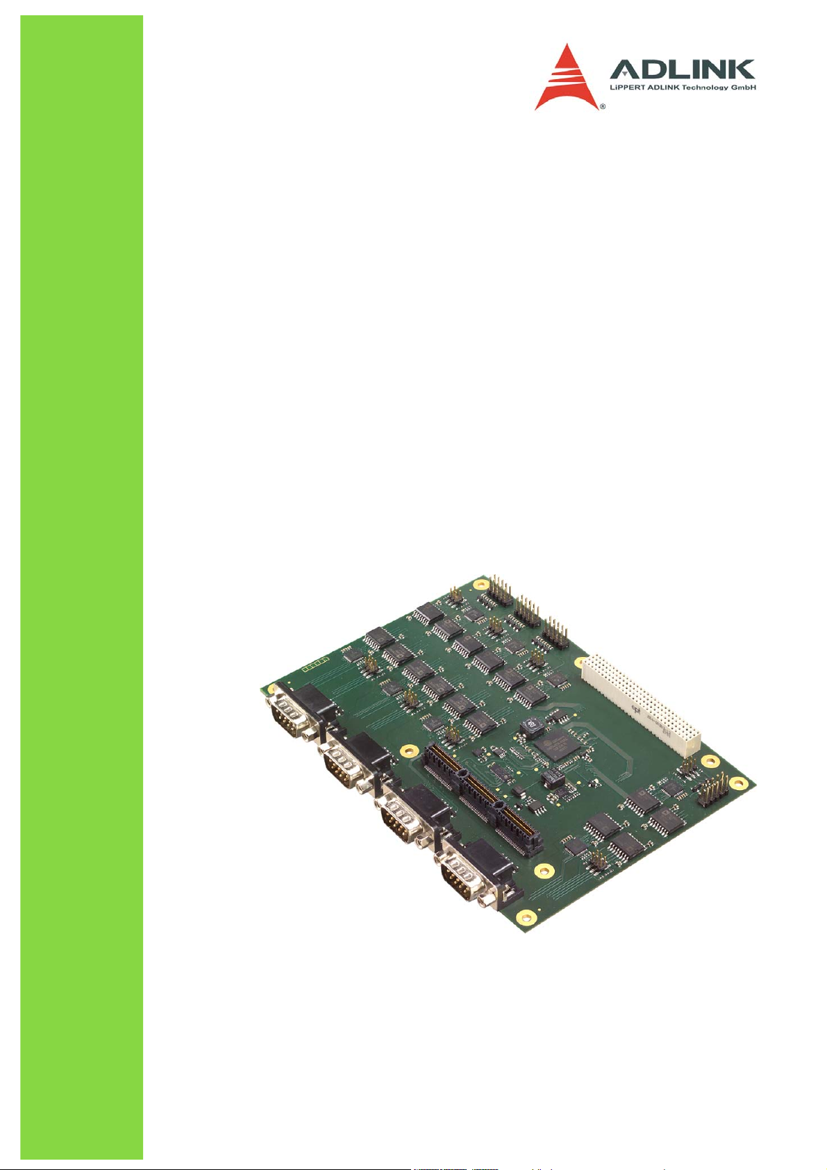
EXP-ISO-COM8
EPIC Express
TM
Add-on-Board
Technical Manual
TME-EXP-ISO-COM8-R1V0
Revision 1.0 / February 14
©LiPPERT Adlink Technology GmbH
Hans-Thoma-Str. 11
D-68163 Mannheim
http://www.adlinktech.com
Page 2

Technical Manual EXP-ISO-COM8
LiPPERT Document: TME-EXP-ISO-COM8-R1V0 Revision 1.0
Copyright © 2009 LiPPERT Adlink Technology GmbH, All rights reserved
Contents and specifications within this manual are subject of change without notice.
Trademarks
Windows XP is a trademark of Microsoft Corporation. EPIC Express is a registered trademark of PC/104
Consortium. All other trademarks appearing in this document are the property of their respective owners.
Page 3

Table of Contents
1 Overview 1
1.1 Introduction ................................................................................................................................. 1
Features .................................................................................................................................................................... 1
Block Diagram ........................................................................................................................................................ 2
1.2 Ordering Information ................................................................................................................ 3
EXP-ISO-COM8 Models ..................................................................................................................................... 3
Cable Sets and Accessories .............................................................................................................................. 3
1.3 Specifications ............................................................................................................................... 4
Electrical Specifications ...................................................................................................................................... 4
Environmental Specifications ........................................................................................................................... 4
Mean Time Between Failures ........................................................................................................................... 4
Mechanical ............................................................................................................................................... 5
Getting Started 8
1.4 Connector Locations .................................................................................................................. 8
Top .............................................................................................................................................................................. 8
Bottom ...................................................................................................................................................................... 9
1.5 Jumper Locations...................................................................................................................... 11
1.6 LED indicators ........................................................................................................................... 12
1.7 Hardware Setup ........................................................................................................................ 13
1.8 Software Setup .......................................................................................................................... 14
TME-EXP-ISO-COM8-R1V0 Rev 1.0 i
Page 4

2 Module Description 15
2.1 OXPCIe958 ................................................................................................................................. 15
Serial Ports ............................................................................................................................................................ 15
DSUB-9 Connectors ........................................................................................................................................... 15
IDC10 Connectors .............................................................................................................................................. 15
RS485-Selection and Termination Jumpers ............................................................................................. 17
2.2 PC/104-Plus Bus Connector .................................................................................................... 18
2.3 PCI/104 Express Bus Interface ............................................................................................... 20
Top PCI/104-Express Connector ................................................................................................................... 20
Bottom PCI/104-Express Connector ........................................................................................................... 22
2.4 Port Isolation ............................................................................................................................. 24
Appendix A, Contact Information A
Appendix B, Additional Information B
Appendix C, Getting Help C
Appendix D, Revision History D
TME-EXP-ISO-COM8-R1V0 Rev 1.0 ii
Page 5

Acronyms
CTS Clear To Send
DCD Data Carrier Detect
DSR Data Set Ready
DTR Data Terminal Ready
FIFO First In First Out
GND Ground
ISO-GND Isolated Ground
MSI-Extend Message Signaled Interrupts - Extend
PCB Printed Circuit Board
PCI Peripheral Component Interconnect
PCIe Peripheral Component Interconnect Express
RI Ring Indicator
RTS Request To Send
RxD Received Data
SerDes Serializer/Deserializer
TxD Transmitted Data
USB Universal Serial Bus
TME-EXP-ISO-COM8-R1V0 Rev 1.0 iii
Page 6

1 Overview
1.1 Introduction
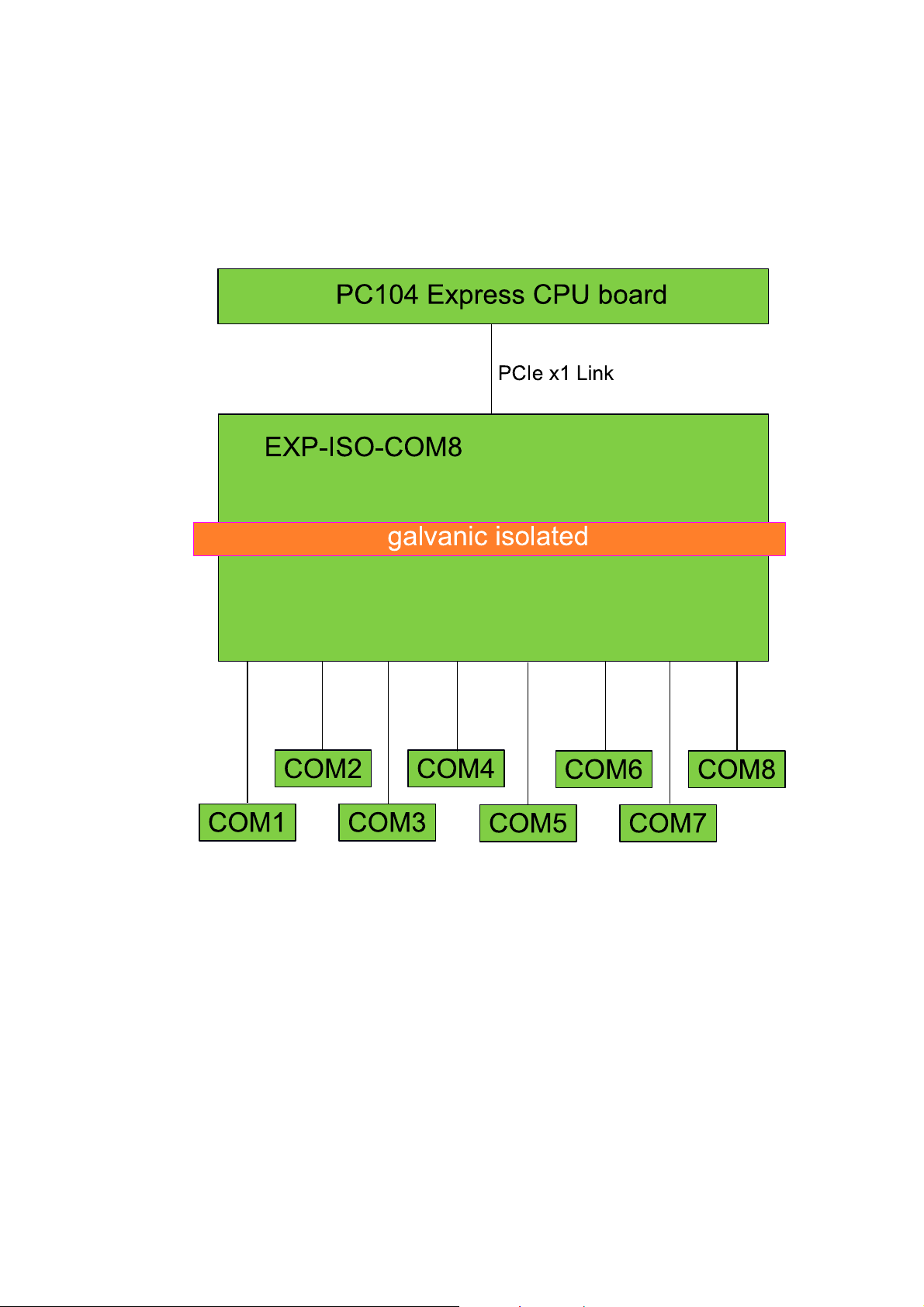
The EXP-ISO-COM8 is an Add-on Module conforming to the EPIC Express Specification. It comprises eight
independent serial ports with RS232 / RS422 / RS485 standards.
Especially for the embedded market all interfaces are galvanic isolated that external distortions cannot
damage the whole Module as well as the CPU board. The galvanic isolation is a good solution for potential
differences with interconnections.
The EXP-ISO-COM8 supports Stack-up and Stack-down to a CPU Module.
The different modes RS232/RS485 for the serial transceivers can be selected by setting a 2.00 mm jumper close
to each interface. The same can be done with termination resistors for RS422 / RS485 mode. Four serial ports
can be found at the front in form of DSUB-9 connectors. The other four are available on IDC10 pin headers.
Furthermore the EXP-ISO-COM8 runs out of a single 5 Volts power supply coming from the PCI/104 Express
connector. All other voltages are generated on the board itself.
The EXP-ISO-COM8 runs with Linux and Windows XP operation systems.
Features
Serial Ports
High-performance Oxford Semiconductor 950
UARTs
Asynchronous baud rate
up to 4Mbps in RS485 mode
up to 460 Kbps in RS232 mode
128-byte deep transmit/receive FIFOs
9, 8, 7, 6 & 5- bit data framing
Flexible clock prescaler from 1 to 31.875
Automated in-band, Xon/Xoff flow control
Automated hardware flow control
Advanced FIFO fill management
RS232, RS422, RS485 operation
Programmable RS485 turn-around delay
450 through 950 software compatibility
PCI Express
Single lane with integrated SerDes
PCI Express bas spec 1.1 compliant
PCI Power Management 1.2 compliant
MSI/MSI-X compatible
DMA/bus mastering facility for all UARTs
ASPM (L0S, L1) Link power management
TME-EXP-ISO-COM8-R1V0 Rev 1.0 1 (24)
Page 7
Block Diagram
TME-EXP-ISO-COM8-R1V0 Rev 1.0 2 (24)
Page 8

1.2 Ordering Information
EXP-ISO-COM8 Models
Order number Description
714-0002-10 EXP-ISO-COM8 with galvanic isolated serial ports
Commercial operating temp. range: 0°C…+60°C
814-0002-10 EXP-ISO-COM8 with galvanic isolated serial ports
Industrial operating temp. range: -20°C…+60°C
914-0002-10 EXP-ISO-COM8 with galvanic isolated serial ports
Extended operating temp. range: -40°C…+85°C
Cable Sets and Accessories
There are some options offered for the EXP-ISO-COM8.
Order number Description
862-0007-10 Adapter Cable, IDC10 (2.54mm) to DSUB9 (COM), 200mm length
TME-EXP-ISO-COM8-R1V0 Rev 1.0 3 (24)
Page 9

1.3 Specifications
Electrical Specifications
Supply voltage +5 V DC
Rise time < 10 ms
Supply voltage tolerance ± 5% *
Supply current maximal 0,5 A (with transfer on all 8 ports at the same time)
typical 0,4 A (with transfer on 4 ports at the same time)
minimal 0,36 A (with no transfer)
Environmental Specifications
Operating:
Temperature range 0 … 60 °C (commercial version)
-20 … 60 °C (industrial version)
-40 … 85 °C (extended version)
Temperature change max. 10K / 30 minutes
Humidity (relative) 10 … 90 % (non-condensing)
Pressure 450 … 1100 hPa
Non-Operating/Storage/Transport:
Temperature range -40 … 85 °C
Temperature change max. 10K / 30 minutes
Humidity (relative) 5 … 95 % (non-condensing)
Pressure 450 … 1100 hPa
Mean Time Between Failures
MTBF at 25°C 713.269 hours
TME-EXP-ISO-COM8-R1V0 Rev 1.0 4 (24)
Page 10

Mechanical
Dimensions (L x W) 165 mm x 115 mm
Height max. 17 mm on top side above PCB
max. 12 mm on bottom side above PCB
Weight 168 g
Mounting 4 mounting holes
Board-to-Board Stacking
height
22 mm
Note: It is strongly recommend using plastic spacers instead of metal spacers to mount
the board. With metal spacers, there is a possible danger to create a short circuit
with the components located around the mounting holes.
This can damage the board!
TME-EXP-ISO-COM8-R1V0 Rev 1.0 5 (24)
Page 11

O
Me
c
v
m
0
i
i
e
0
d
t
a
a
e
s
a
2
Front
Side
Syste
hanical v
view
iew
stack-up v
ew
ew with Hurr
icane-QM57
nd heat spr
ader
TME-EXP-IS
-COM8-R1V
Not
For detaile
departmen
mechanical
.
drawings or
Rev 1.0
tep files ple
se contact our support
6 (
4)
Page 12

Metrics on Top
The connectors' pin 1 is marked with an arrow.
TME-EXP-ISO-COM8-R1V0 Rev 1.0 7 (24)
Page 13

Getting Started
1.4 Connector Locations
Top
Port 8
Port 7
Port 4
Port 3
Port 2
Port 6
X10
Port 5
The connectors' pin 1 is marked with an arrow.
PCI/104
Express
PC/104
Port 1
TME-EXP-ISO-COM8-R1V0 Rev 1.0 8 (24)
Page 14

Bottom
PCI/104
Express
PC/104
TME-EXP-ISO-COM8-R1V0 Rev 1.0 9 (24)
Page 15

TME-EXP-ISO-COM8-R1V0 Rev 1.0 10 (24)
Page 16

1.5 Jumper Locations
Port 8
Port 7
Port 6
Port 4
Port 3
Port 2
Port 1
Port 5
The connectors' pin 1 is marked with an arrow.
TME-EXP-ISO-COM8-R1V0 Rev 1.0 11 (24)
Page 17

O
1.6 LED
o
w
0
r
a
o
0
t
e
Onb
the
indicato
ard there is
orking state
s
yellow LED
f the OXPCI
hat shows
chip.
TME-EXP-IS
-COM8-R1V
Rev 1.0
12 (2 4)
Page 18
1.7 Hardware Setup
Caution Be sure to observe the EMC security measures. Make sure you are always at
Caution Do never connect or disconnect the EXP-ISO-COM8 Add-on Module with a
Be sure that your power supply is able to provide enough current to your system. An insufficient power supply
leads to an instable system.
The EXP-ISO-COM8 does not need any cooling devices.
the same potential as the module.
CPU board while that is running.
TME-EXP-ISO-COM8-R1V0 Rev 1.0 13 (24)
Page 19

1.8 Software Setup
Driver packages are available for the following operating systems:
Linux
Windows XP
Please contact our support department support@lippertembedded.com or have a look at the website
www.lippertmebedded.com for downloading the necessary drivers. Installation guide and all necessary
information is provided in the driver package.
TME-EXP-ISO-COM8-R1V0 Rev 1.0 14 (24)
Page 20

2 Module Description
2.1 OXPCIe958
The device combines a fully integrated, single-lane PCI Express end-point controller and SerDes with eight
high-performance 950 UART.
The OXPCIe958 achieves outstanding performance including 128 byte transmit and receive FIFOs of the 950
UART, with advanced system management features such as MSI/MSI-X interrupt handling and bus master DMA
to maximize data throughput while substantially reducing CPU and system overheads. Each 950 UART has full
modem interface and includes advanced features such as hardware-accelerated out-of-band and in-band flow
control, readable FIFO levels and RS485 turnaround delay for further performance optimization, while the
flexible clock prescaler provides scope for the widest-possible range of baud rates.
Serial Ports
Four serial ports are conducted to DSUB-9 connectors at the front side. The other four serial ports are available
on IDC10 pin headers which can be used with the help of adapter cables provided by Lippert. All ports can
either work in RS232 or in RS485 mode. That mode can be switched with jumpers at runtime, the location can
be found in chapter jumper.
DSUB-9 Connectors
Connector type D-SUB9, male
IDC10 Connectors
Pin RS232 RS485 Pin RS232 RS485
1 DCD Not used 6 DSR RXD+
2
RXD RXD- 7 RTS TXD+
3
TXD TXD- 8 CTS Not used
4
DTR Not used 9 RI Not used
5
ISOGND ISOGND Shield Not used Not used
1
6
Connector type IDC10 pin header 2.54 mm
TME-EXP-ISO-COM8-R1V0 Rev 1.0 15 (24)
Page 21

Pin RS232 RS485 Pin RS232 RS485
1 DCD
3 RXD RXD- 4 RTS TXD+
5 TXD TXD- 6 CTS Not used
7 DTR Not used 8 RI Not used
9 ISOGND ISOGND 10 Not used Not used
Not used
2 DSR RXD+
Pin 1 is marked with a small arrow
TME-EXP-ISO-COM8-R1V0 Rev 1.0 16 (24)
Page 22

O
RS4
8
e
2
R
e
n
e
R
d
8
e
0
n
s
a
R
i
v
i
h
o
d
d
n
a
e
f
e
3
s
h
p
t
a
d
n
I
h
t
o
e
i
e
a
s
-RX+
a
Conn
Use
The
For s
5-Selectio
ctor type
mm jumper
S485 termin
lecting the
and Termi
IDC6 pin he
to terminat
tion jumpers
S485 mode t
ation Jum
der 2.00 mm
lines correc
are located
he pins 5 an
ers
ly.
t the top of
6 at each p
he printed c
rt have to b
rcuit board,
shorted.
ee chapter 1
5
Pin
1
3
5
Whe
the jumper
are t
rminated wit
(e.g.
Addit
ionally, positi
pulle
order
COM
It is r
Signal
TX+
RX+
RS485 mo
X+ and RX-)
up/down w
to protect t
from overv
commende
Pin
2
4
e 6
s set, the dif
h 120 betw
e/negative r
th 10 k to
e transceiver
ltage.
to protect t
Signal
TX-
RX-
VCC
erential pairs
en them.
ceive lines a
,3 V/ GND i
of the EXP-
e ports of t
re
SO-
e external d
RX+
UART
RX-
vice in the s
10 k
120
10 k
me way!
3,3 V
Jumper
GND
extern
devic
RX
l
e
TME-EXP-IS
-COM8-R1V
Rev 1.0
17 (2
4)
Page 23

2.2 PC/104-Plus Bus Connector
The PC/104-plus bus is not used on that module. The mounted connector forward the signal through.
Pin A B C D
1 GND n.c. n.c. n.c.
2 n.c. n.c. n.c. n.c.
3 n.c. GND n.c. n.c.
4 n.c. n.c. GND n.c.
5 GND n.c. n.c. GND
6 n.c. n.c. n.c. n.c.
7 n.c. n.c. GND n.c.
8 n.c. n.c. n.c. n.c.
9 n.c. GND n.c. n.c.
10 GND n.c. n.c. n.c.
11 n.c. n.c. n.c. GND
12 n.c. n.c. GND n.c.
13 n.c. GND n.c. n.c.
14 GND n.c. n.c. n.c.
15 n.c. n.c. n.c. GND
16 n.c. n.c. GND n.c.
17 n.c. n.c. n.c. n.c.
18 n.c. GND n.c. n.c.
19 n.c. n.c. n.c. n.c.
20 GND n.c. n.c. GND
21 n.c. n.c. n.c. n.c.
22 n.c. n.c. GND n.c.
23 n.c. GND n.c. n.c.
24 GND n.c. n.c. n.c.
25 n.c. n.c. n.c. GND
TME-EXP-ISO-COM8-R1V0 Rev 1.0 18 (24)
Page 24

Pin A B C D
26 n.c. n.c. GND n.c.
27 n.c. n.c. n.c. GND
28 GND n.c. n.c. n.c.
29 n.c. n.c. n.c. n.c.
30 n.c. n.c. n.c. GND
TME-EXP-ISO-COM8-R1V0 Rev 1.0 19 (24)
Page 25

2.3 PCI/104 Express Bus Interface
The EXP-ISO-COM8 uses x1 link of the PCI/104-Express bus. According to the EPIC Express specification it
depends on the stacking position above or below the CPU board which link is used. On the module there is a
PCI Express switch that detects the type of connection and forwards the other links according to the
specification.
Top PCI/104-Express Connector
Connector Type: Samtec ASP-142781-05
PIN Signal PIN Signal
1
3
5
7
9
11
13
15
17
19
21
23
25
27
29
31
33
35
37
39
41
43
45
47
49
51
+3.3V
USB_1+
USB_1-
GND
Pex1_1Tp
Pex1_1Tn
GND
Pex1_2 Tp
Pex1_2 Tn
GND
Pex1_1Rp
Pex1_1Rn
GND
Pex1_2 Rp
Pex1_2 Rn
GND
Pex1_1Clkp
Pex1_1Clkn
+5V_Always
Pex1_2Clkp
Pex1_2Clkn
CPU_DIR
SMB_DAT
SMB_CLK
SMB_ALERT
2
4
6
8
10
12
14
16
18
20
22
24
26
+5V
28
30
32
34
36
38
40
42
44
46
48
50
52
+3.3V
USB_0+
USB_0-
GND
Pex1_0 Tp
Pex1_0 Tn
GND
Pex1_3 Tp
Pex1_3 Tn
GND
Pex1_0 Rp
Pex1_0 Rn
GND
Pex1_3 Rp
Pex1_3 Rn
GND
Pex1_0Clkp
Pex1_0Clkn
+5V_Always
Pex1_3Clkp
Pex1_3Clkn
PWRGOOD
Pex16_Clkp
Pex16_Clkn
PSON#
The blue highlighted signals are used by the OXPCIe958 chip, if the EXP-ISO-COM8 is stacked below the CPU
(stacked-down).
TME-EXP-ISO-COM8-R1V0 Rev 1.0 20 (24)
Page 26

The following table shows the shifting of PCI Express links from top to bottom connector.
The rest of not listed PCI/104 Express pins are directly forwarded.
PCI/104 Express TOP Bottom
OXPCIe958 3x1 link -
shifted 2x1 link 3x1 link
shifted 1x1 link 2x1 link
shifted 1x0 link 1x1 link
TME-EXP-ISO-COM8-R1V0 Rev 1.0 21 (24)
Page 27

Bottom PCI/104-Express Connector
Connector Type: Samtec ASP-129646-03
PIN Signal PIN Signal
1
3
5
7
9
11
13
15
17
19
21
23
25
27
29
31
33
35
37
39
41
43
45
47
49
51
+3.3V
USB_1+
USB_1-
GND
Pex1_1Tp
Pex1_1Tn
GND
Pex1_2 Tp
Pex1_2 Tn
GND
Pex1_1Rp
Pex1_1Rn
GND
Pex1_2 Rp
Pex1_2 Rn
GND
Pex1_1Clkp
Pex1_1Clkn
+5V_Always
Pex1_2Clkp
Pex1_2Clkn
CPU_DIR
SMB_DAT
SMB_CLK
SMB_ALERT
2
4
6
8
10
12
14
16
18
20
22
24
26
+5V
28
30
32
34
36
38
40
42
44
46
48
50
52
+3.3V
USB_0+
USB_0-
GND
Pex1_0 Tp
Pex1_0 Tn
GND
Pex1_3 Tp
Pex1_3 Tn
GND
Pex1_0 Rp
Pex1_0 Rn
GND
Pex1_3 Rp
Pex1_3 Rn
GND
Pex1_0Clkp
Pex1_0Clkn
+5V_Always
Pex1_3Clkp
Pex1_3Clkn
PWRGOOD
Pex16_Clkp
Pex16_Clkn
PSON#
The blue highlighted signals are used by the OXPCIe958 chip, if the EXP-ISO-COM8 is stacked above the CPU
(stacked-up).
The following table shows the shifting of PCI Express links from bottom to top connector.
The rest of not listed PCI/104 Express pins are directly forwarded.
PCI/104-Express Connector Bottom TOP
OXPCIe958 0x1 link -
shifted 1x1 link 0x1 link
shifted 2x1 link 1x1 link
shifted 3x1 link 2x1 link
TME-EXP-ISO-COM8-R1V0 Rev 1.0 22 (24)
Page 28

TME-EXP-ISO-COM8-R1V0 Rev 1.0 23 (24)
Page 29

O
2.4 Por
t
s
M
n
u
u
g
O
O
0
n
D
s
m
w
m
p
m
n
m
1
e
v
h
q
a
e
h
d
h
t
o
w
r
u
n
c
c
Each
ADu
galva
GND
Isolatio
serial port is
5401 and A
ic isolated. I
and Data.
extra isolated
uM5404 fro
n conclusion
. Onboard th
Analog De
there are eig
ere are two
ices the dat
ht separated
uad channel
channels ar
zones with t
isolators for
optical und
eir own pote
ne COM po
the power s
ntial regardi
t. With the
pply is
g to VCC,
Feat
AD
Hi
S
25
V
re
M540x
h common-
IC package
00 Vs for 1
= 560 V
I
RM
ode transie
ith > 8.0 m
inute per UL
eak
t immunity:
creepage
577
> 25 kV/µs
PCB
separate
throug
and to
I/O zones
out all layers
he common
ith > 3 mm
between ea
interface
reepage
h other
TME-EXP-IS
-COM8-R1V
Rev 1.0
24 (2
4)
Page 30

Appendix A, Contact Information
Headquarters
LiPPERT ADLINK Technology GmbH
Hans-Thoma-Straße 11
68163 Mannheim
Germany
Phone +49 621 43214-0
Fax +49 621 4321430
E-mail sales: emea@adlinktech.com
Support: helpdesk@adlinktech.com
RMA: RMA.EMEA@adlinktech.com
Website http://www.adlinktech.com/rugged/index.php
TME-EXP-ISO-COM8-R1V0 Rev 1.0 Appendix A
Page 31

Appendix B, Additional Information
B.1 Additional Reading
Datasheet of the OXPCIe958 at http://www.plxtech.com
B.2 PCI/104 ExpressTM
A copy of the latest PCI/104 Express and can be obtained from the PC/104 Consortium's website at
www.pc104.org
TME-EXP-ISO-COM8-R1V0 Rev 1.0 Appendix B
Page 32

Appendix C, Getting Help
Should you have technical questions that are not covered by the respective manuals, please contact our
support department at http://askanexpert.adlinktech.com .
Please allow one working day for an answer.
Returning Products for Repair
To return a product to ADLINK Technology GmbH for repair, you need to get a Return Material Authorization
(RMA) number first.
Please print the RMA Request Form from http://www.adlinktech.com/lippert/rma.php
fill in the blanks and fax it to +49 621 4321430. We'll return it to you with the RMA number.
For further RMA requests use this RMA email: RMA.EMEA@adlinktech.com
Caution: Deliveries without a valid RMA number are returned to sender at his or her own cost.
TME-EXP-ISO-COM8-R1V0 Rev 1.0 Appendix C
Page 33

Appendix D, Revision History
Filename Date Edited
by
TME-EXP-ISO-COM8-R0V0.doc 2009-12-10 CS Draft
TME-EXP-ISO-COM8-R0V1.doc 2010-04-12 MF Some minor changes
Driver section added
TME-EXP-ISO-COM8-R0V2.doc 2011-01-18 MF Some minor changes
MTBF value added
TME-EXP-ISO-COM8-R0V3.doc 2011-02-21 MF Mechanical dimensions corrected
part numbers 8xx, 9xx added
Appendix A new US address
TME-EXP-ISO-COM8-R1V0.doc 2014-02-03 MF Ch. 1.4 clarified stacking height 22m, mechanical view
added
Ch. 2.3 SAMTEC part number corrected
Change
TME-EXP-ISO-COM8-R1V0 Rev 1.0 Appendix D
 Loading...