

Page 1

ETX®-PVR
Computer-on-Module
Reference Manual
P/N 50-1Z057-1010
Page 2

Notice Page
DISCLAIMER
ADLINK Technology, Incorporated makes no representations or warranties with respect to the contents of
this manual or of the associated ADLINK products, and specifically disclaims any implied warranties of
merchantability or fitness for any particular purpose. ADLINK shall under no circumstances be liable for
incidental or consequential damages or related expenses resulting from the use of this product, even if it has
been notified of the possibility of such damages. ADLINK reserves the right to revise this publication from
time to time without obligation to notify any person of such revisions. If errors are found, please contact
ADLINK at the address shown at the bottom of this page.
TRADEMARKS
CoreModule and the Ampro logo are registered trademarks, and ADLINK, Little Board, LittleBoard,
MightyBoard, MightySystem, MilSystem, MiniModule, ReadyBoard, ReadyBox, ReadyPanel,
ReadySystem, and RuffSystem are trademarks of ADLINK Technology, Inc. All other marks are the
property of their respective companies.
REVISION HISTORY
Revision Reason for Change Date
1000 Initial Release Nov/10
1010 Replaced N450, D410, and D510 CPUs with N455 and D525;
upgraded DDR2 memory to DDR3; revised definition of JP1 from
Clear CMOS to SSD Select; added U20 Temperature Sensor; revised
DASP and PDIAG signals in Tab le 3- 8; revised various sections of
ch 4; added Figures 2-9, 2-10, and 2-11 to illustrate In-Rush power
consumption
Aug/12
ADLINK Technology, Incorporated
5215 Hellyer Avenue, #110
San Jose, CA 95138-1007
Tel. 408 360-0200
Fax 408 360-0222
www.adlinktech.com
© Copyright 2010, 2011, 2012 ADLINK Technology, Incorporated
Audience
This manual provides reference only for computer design engineers, including but not limited to hardware
and software designers and applications engineers. ADLINK Technology, Inc. assumes you are qualified to
design and implement prototype computer equipment.
ii Reference Manual ETX-PVR
Page 3

Contents
Chapter 1 About This Manual ....................................................................................................1
Purpose of this Manual ....................................................................................................................1
References ......................................................................................................................................1
Chapter 2 Product Overview......................................................................................................3
ETX Computer-on-Module Concept.................................................................................................3
Product Description..........................................................................................................................4
Board Features ..........................................................................................................................5
Block Diagram ............................................................................................................................7
Major Components (ICs)..................................................................................................................8
Connector and Socket Definitions..................................................................................................10
Jumper Header Definition ......................................................................................................12
Specifications ................................................................................................................................13
Physical Specifications ............................................................................................................13
Mechanical Specifications ........................................................................................................13
Environmental Specifications ...................................................................................................14
Power Specifications .............................................................................................................14
Thermal/Cooling Requirements .........................................................................................17
Chapter 3 Hardware ...............................................................................................................19
Overview ........................................................................................................................................19
CPU ...............................................................................................................................................20
Graphics ........................................................................................................................................20
Memory .........................................................................................................................................20
Interrupt Channel Assignments (IRQs) ..........................................................................................21
Memory Map .................................................................................................................................22
I/O Address Map ...........................................................................................................................22
X1 PCI Bus Interface (J1) .............................................................................................................23
PCI Bus ....................................................................................................................................23
Universal Serial Bus (USB) ......................................................................................................23
Serial Interrupt Request ...........................................................................................................23
Audio Interface .........................................................................................................................24
X2 ISA Bus Interface (J2) ...........................................................................................................27
X3 Primary I/O Interface (J3) ........................................................................................................31
Floppy Interface .......................................................................................................................31
Parallel Interface ......................................................................................................................31
Serial Ports 1 and 2 .................................................................................................................31
PS/2 Keyboard .........................................................................................................................31
PS/2 Mouse .............................................................................................................................31
VGA Interface ..........................................................................................................................31
LVDS Interface ........................................................................................................................32
X4 IDE and Auxiliary Interface (J4) ...............................................................................................36
IDE Port .................................................................................................................................36
Ethernet Port Interface..............................................................................................................36
Power Control Signals .............................................................................................................37
Power Management Signals ....................................................................................................37
Speaker ...................................................................................................................................37
Real Time Clock (RTC) .........................................................................................................37
SMBus ...................................................................................................................................38
ETX-PVR Reference Manual iii
Page 4

Contents
Miscellaneous ............................................................................................................................... 42
Oops! Jumper (BIOS Recovery) ............................................................................................. 42
Remote Access ...................................................................................................................... 42
Remote Access Setup ........................................................................................................ 42
Hot (Serial) Cable .............................................................................................................. 42
Temperature Monitoring .......................................................................................................... 42
Watchdog Timer (WDT) ........................................................................................................... 43
Power Interface ............................................................................................................................. 43
Power and Sleep States................................................................................................................ 43
Power-On Switch .................................................................................................................... 43
Sleep States (ACPI) ................................................................................................................. 44
Chapter 4 BIOS Setup .............................................................................................................. 47
Introduction.................................................................................................................................... 47
Entering BIOS Setup (Local Video Display) ............................................................................. 47
Entering BIOS Setup (Remote Access) .................................................................................. 47
PCI-ISA Bridge Mapping ............................................................................................................... 48
Logo Screen Utility (Splash Screen) .............................................................................................48
Logo Screen Image Requirements ......................................................................................... 48
BIOS Setup Menus ....................................................................................................................... 49
BIOS Main Setup Screen ........................................................................................................ 49
BIOS Advanced Setup Screen ................................................................................................ 50
BIOS Power Management Setup Screen ................................................................................ 53
BIOS Boot Setup Screen ........................................................................................................ 54
BIOS Security Setup Screen ................................................................................................... 56
BIOS Exit Setup Screen .......................................................................................................... 57
Appendix A Technical Support ..................................................................................................59
Index .................................................................................................................................................. 61
List of Figures
Figure 2-1. ETX-PVR Module and Custom Baseboard Assembly............................................. 3
Figure 2-2. Typical ETX Design Flow ........................................................................................ 4
Figure 2-3. Functional Block Diagram ....................................................................................... 7
Figure 2-4. Component Locations (Top Side)............................................................................ 9
Figure 2-5. Component Locations (Bottom Side) .................................................................... 10
Figure 2-6. Connector and Socket Locations (Top Side)......................................................... 11
Figure 2-7. Connector Locations (Bottom Side) ...................................................................... 12
Figure 2-8. Mechanical Overview (Bottom Side) ..................................................................... 13
Figure 2-9. N455 (with SpeedStep disabled) Peak In-Rush Current and Duration ................. 15
Figure 2-10. N455 Peak In-Rush Current and Duration ............................................................ 15
Figure 2-11. D525 Peak In-Rush Current and Duration ............................................................ 16
Figure 2-12. Stack Heights of Cooling Assemblies.................................................................... 17
Figure 3-1. Oops! Jumper Connection..................................................................................... 42
Figure 3-2. Hot Cable Jumper ................................................................................................. 42
Figure 4-1. BIOS Main Setup Screen ...................................................................................... 49
Figure 4-2. BIOS Advanced Setup Screen .............................................................................. 50
Figure 4-3. Power Management Setup Screen ....................................................................... 53
Figure 4-4. BIOS Boot Setup Screen....................................................................................... 54
Figure 4-5. BIOS Security Setup Screen ................................................................................. 56
Figure 4-6. BIOS Exit Setup Screen ........................................................................................ 57
iv Reference Manual ETX-PVR
Page 5

List of Tables
Table 2-1. Major Components Descriptions and Functions ......................................................8
Table 2-2. Connector and Socket Descriptions.......................................................................10
Table 2-3. Jumper Header Setting ..........................................................................................12
Table 2-4. Weight and Footprint Dimensions..........................................................................13
Table 2-5. Environmental Requirements.................................................................................14
Table 2-6. Power Supply Requirements .................................................................................14
Table 2-7. ADLINK Optional Cooling Solutions.......................................................................17
Table 3-1. Interrupt Channel (IRQs) Assignments (Typical) ...................................................21
Table 3-2. Memory Map ..........................................................................................................22
Table 3-3. I/O Address Map ....................................................................................................22
Table 3-4. Complete X1 Interface Pin Signal Descriptions (J1) ..............................................24
Table 3-5. Complete X2 ISA Bus Interface Pin Signal Descriptions (J2) ................................27
Table 3-6. Complete X3 Interface Pin Signal Descriptions (J3) ..............................................32
Table 3-7. SMBus Reserved Addresses .................................................................................38
Table 3-8. Complete X4 Interface Pin Signal Descriptions (J4) ..............................................38
Table 4-1. BIOS Setup Menus ................................................................................................49
Table A-1. Technical Support Contact Information..................................................................59
Contents
ETX-PVR Reference Manual v
Page 6

Contents
vi Reference Manual ETX-PVR
Page 7

Chapter 1 About This Manual
Purpose of this Manual
This manual is for designers of systems based on the ETX®-PVR Computer-on-Module (COM). This
manual contains information that permits designers to create an embedded system based on specific design
requirements.
Information provided in this reference manual includes:
• Product Overview
• Hardware Specifications
• Technical Support Contact Information
Information not provided in this reference manual includes:
• Detailed chip specifications
• Internal component operation
• Internal registers or signal operations
• Bus or signal timing for industry standard busses and signals
• Pinout definitions for industry standard interfaces
References
The references in the following list may help you successfully complete your custom design.
Specifications:
• ETX Spec Revision 3.02, 2007
For the latest version of the ETX specifications, use the web page at:
Web site: http://www.etx-ig.org/specs/specs.php
• PCI 2.3 Compliant Specifications
For latest revision of the PCI specifications, contact the PCI Special Interest Group Office at:
Web site: http://www.pcisig.com
• AMI BIOS Core 8 User’s Guide
Web site: http://www.ami.com/support/doc/MAN-EZP-80.pdf
Chip specifications:
• Intel Corporation and the Atom N400 and D500 series processors (with integrated Northbridge)
Web site: http://www.intel.com/p/en_US/embedded/hwsw/hardware/atom-400-500/hardware
• Intel Corporation and the ICH8-M chip, 82801HM, used for the I/O Hub (Southbridge)
Data sheet: http://www.intel.com/assets/pdf/datasheet/313056.pdf
• Intel Corporation and the 82567V chip, used as Ethernet transceiver
Data sheet: http://download.intel.com/design/network/datashts/82567.pdf
• SMSC and the SCH3112I-NU chip used for the Super I/O controller
Data sheet: http://www.smsc.com/media/Downloads_Public/Data_Briefs/311xdb.pdf
ETX-PVR Reference Manual 1
Page 8

Chapter 1 About This Manual
• Realtek and the ALC262-VD2-GR chip, used for the Audio CODEC
Web site: http://www.realtek.com/search/default.aspx?keyword=alc262
• ITE Tech. Inc. and the IT8888G-L chip, used for the PCI-to-ISA bridge conversion
Web site: http://www.ite.com.tw/EN/products_more.aspx?CategoryID=3&ID=5,76
• Greenliant and the GLS85LP1004P Solid State Drive (SSD)
Web site: http://www.greenliant.com/products/?inode=46780
• ON Semiconductor and the ADT7481ARMZ Temperature Sensor
Data sheet: http://www.onsemi.com/pub_link/Collateral/ADT7481-D.PDF
• Atmel Corporation and the ATMEGA168V-10AU micro controller, used as the board controller
Data sheet: http://www.atmel.com/dyn/resources/prod_documents/doc8025.pdf
NOTE If you are unable to locate the datasheets using the links provided, search the
internet to find the manufacturer’s web site and locate the documents you need.
2 Reference Manual ETX-PVR
Page 9
Chapter 2 Product Overview
ETX-PVR_Stack
ETX-PVR Computer -on -Module
Custom Baseboard Design
Stack Connectors
(4 pairs)
M2.5 PEM Nuts
Spacing 3 mm (4)
M2.5 Screws (4)
This introduction presents general information about the ETX Architecture and the ETX-PVR Computeron-Module (COM). After reading this chapter you should understand:
• ETX Computer-on-Module concept
• ETX-PVR product description
• ETX-PVR features
• Major components
• Connectors
• Specifications
ETX Computer-on-Module Concept
Embedded system designers face increasing pressures to bring products to market quickly. Many products
that once incorporated a custom CPU design can no longer afford the time to develop and debug a custom
CPU let alone port operating system software to it. Furthermore, CPU subsystem design usually plays a
small part in providing any uniqueness to an embedded product. The remainder of the embedded product
design adds key circuits that provide a unique product and differentiate it from other products serving the
same market. The challenge is to speed these designs to market by eliminating the need for a custom CPU
design while providing the flexibility to include all critical elements, which make the embedded product
unique.
The Embedded Technology eXtended (ETX) module provides an off-the-shelf CPU subsystem that can be
included in virtually any embedded system. An ETX module works like a high-integration chip, plugging
into your custom circuit board design to provide specific control for your logic application. See Figure 2-1.
Figure 2-1. ETX-PVR Module and Custom Baseboard Assembly
ETX provides a simple, standard interface that is independent of CPU type. The ETX interface includes the
industry-standard PCI bus, ISA bus (some models), I/O signals from the peripheral components on the ETX
module, power, and ground. Visit the ADLINK web site (www.adlinktech.com
availability and support information.
The standard ETX interface lets you try different processors in your actual product environment with the
ability to defer a processor choice until late in the project if you so choose. The interface also lets you easily
offer different versions of your product with different capabilities by either selecting different ETX modules
with the same baseboard, or by designing different baseboards for the same CPU. This simple ability to
upgrade by either selecting a more powerful CPU (without baseboard redesign) or enhancing the baseboard
without touching the CPU subsystem or the bulk of the applications software.
The ETX flexibility enables designers to take an accelerated, low risk path by using proven ETX module
designs. Your design flow might look similar to the one shown in Figure 2-2. This diagram gives a Typical
Design Flow of hardware and software functions.
) for the latest ETX processor
ETX-PVR Reference Manual 3
Page 10

Chapter 2 Product Overview
CPU and Software
Design Path
Design applicationspecific baseboard
Fabricate baseboard
Debug baseboard
Revise baseboard
if necessary
Integrate application code
Hardware
Design Path
Select CPU
Select OS & Tools
Write and Test
Application Code
Write drivers for
custom Logic
ETXdesignflw
Figure 2-2. Typical ETX Design Flow
Product Description
The ETX-PVR is an exceptionally high integration, high performance, rugged, and high quality Computeron-Module (COM), which contains all the component subsystems of an ATX motherboard plus the
equivalent of up to 2 expansion boards. Based on the Intel® Atom™ N455 and D525 processors, the
ETX-PVR provides designers a complete, high performance embedded processor that conforms to the ETX
V3.02 specification.
The Intel Atom N400 and D400/D500 series CPUs integrate processor cores with Graphics and Memory
Hubs (GMHs), providing low-power, high-performance processors, memory controllers for up to 2GB of
DDR3 memory, and graphics controllers which provide LVDS and VGA signals for most LCD video panels
and CRT monitors.
The ICH8-M chipset provides controllers for the I/O Hub (Southbridge) featuring four USB ports, one Ultra
DMA 33/66/100 IDE port supporting two IDE devices, one HD Audio link, two SATA ports, one Ethernet
interface, one PCI interface, one SMBus interface, one LPC bus, and one speaker port. The ETX-PVR
provides legacy interfaces through the SMSC SCH3112I-NU Super I/O featuring two serial ports, one
parallel/floppy port, and one PS/2 keyboard and mouse port.
Among the many embedded-PC enhancements on the ETX-PVR that ensure embedded system operation
and application versatility are a Watchdog Timer, remote access support, battery-free boot, and OEM logo
customization (Splash Screen).
The ETX-PVR is particularly well suited to either embedded or portable applications and meets the size,
power consumption, temperature range, quality, and reliability demands of embedded system applications.
The ETX-PVR requires a single +5V power supply.
4 Reference Manual ETX-PVR
Page 11

Chapter 2 Product Overview
Board Features
• CPU
Provides Intel Atom 1.66GHz N455 (6.5W) or Atom 1.80GHz D525 (13W) processor cores
DMI (Direct Media Interface) with 1 GB/s of bandwidth in each direction
Enhanced SpeedStep® technology
On die 512-kB, 8-way L2 cache
• Memory
Single standard 204-pin DDR3 SODIMM socket
Supports +1.5V DDR3, 800MHz RAM up to 2GB
Supports only non-ECC memory
Supports only unbuffered memory
• PCI Bus/ISA Bus
PCI 2.3 compliant, 32-bits wide
Supports PCI Bus speed at 33 MHz
Supports ISA bus speed at 8 MHz
• IDE Interfaces
Provides one enhanced IDE controller
Provides soldered Solid State Drive (SSD)
Supports dual bus master mode
Supports Ultra DMA 33/66/100 modes
Supports ATAPI and DVD peripherals
Supports IDE native and ATA compatibility modes
• SATA
Supports two SATA ports from the ICH8-M I/O Hub
Provides two standard SATA connectors
• Floppy Disk Interface
Supports one standard floppy disk drive interface
Supports all standard PC/AT formats: 360KB, 1.2MB, 720KB, 1.44MB, 2.88MB
• Parallel Port
Provides a standard printer interface
Supports IEEE standard 1284 protocols of EPP and ECP outputs
Supports Bi-directional data lines
• Serial Ports
Provide two buffered serial ports with full handshaking
Provide 16550-equivalent controllers, each with a built-in 16-byte FIFO buffer
Support full modem capability
Support RS232 operation
Support programmable word length, stop bits, and parity
Supports 16-bit programmable baud-rate generator and an interrupt generator
ETX-PVR Reference Manual 5
Page 12

Chapter 2 Product Overview
• USB Ports
Provide two root USB hubs
Provide up to four USB ports
Support USB boot devices
Support USB v2.0 EHCI and OHCI v1.1
Support over-current detection status
• Keyboard/Mouse Interface
Provides PS/2 keyboard interface
Provides PS/2 mouse interface
• Audio interface
Provides HD Audio CODEC on board
Supports HD Audio standard
Supports the audio amplifier on the baseboard
• Ethernet Interface
Provides one fully independent Ethernet port
Provides integrated LEDs (Link/Activity and Speed)
Provides Intel 82567V Ethernet transceiver chip
Supports IEEE 802.3 10/100BaseTX compatible physical layers
Supports Auto-negotiation for speed, duplex mode, and flow control
Supports full-duplex or half-duplex mode
• Full-duplex mode supports transmit and receive frames simultaneously
• Supports IEEE 802.3x Flow control in full duplex mode
• Half-duplex mode supports enhanced proprietary collision reduction mode
• Video Interfaces (VGA and LVDS)
Provide VGA outputs (resolutions up to 1400x1050 @ 60Hz for the N455 CPU and 2048x1536 @
60Hz for the D525 CPU)
Provide LVDS flat panel outputs (resolutions up to 1280x800 for the N455 CPU and 1366x768 for
the D525 CPU) [single channel, three differential signals]
• Miscellaneous
Real Time Clock (RTC) with replaceable battery on baseboard
Battery-free boot (Boots even if battery is dead or missing)
Supports external battery for Real Time Clock operation
Oops! Jumper (BIOS recovery) support
Remote Access
Watchdog Timer (WDT)
6 Reference Manual ETX-PVR
Page 13
Chapter 2 Product Overview
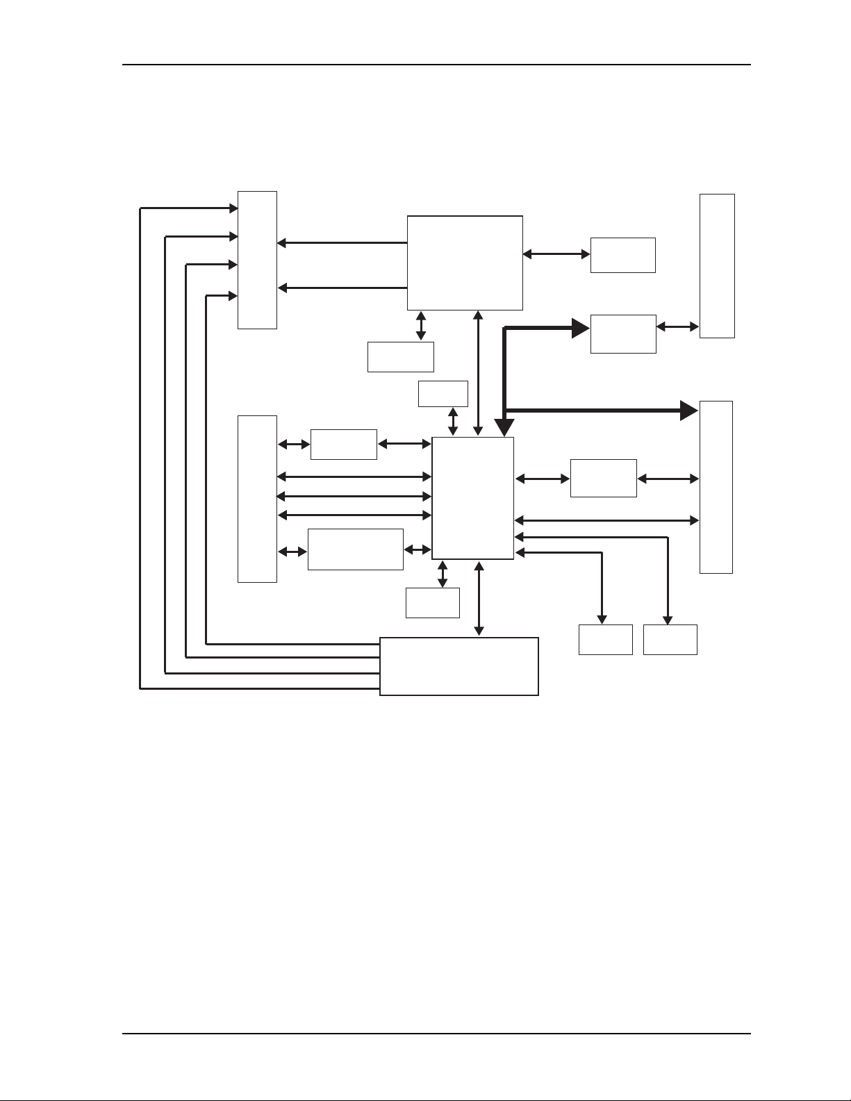
ETX-PVR_Blkdiagm_b
CPU
Intel Atom
1.66GHz N455 (6.5W)
or 1.80GHz D525 (13W)
(with Integrated
Video and Memory)
DDR3
SODIMM
PS/2 Keyboard/Mouse
PCI -to-ISA
Bridge
IT8888G-L
PCI Bus
(32bit / 33MHz)
DMI (4)
Parallel/Floppy Port
Serial Port I/F
HD Audio
ALC262
Temperature
Sensor
USB 2.0 (4)
Super I/O
SCH3112I-NU
HDA Link
Line In/Out,
MIC
X3
Connector (J3)
X2
Connector (J2)
X1
Connector (J1)
X4
Connector (J4)
Ethernet Transceiver
Intel 82567V
GbE PHY
Solid State
Drive
Board
Controller
SATA1
Connector
BIOS
SATA2
Connector
IrDA
I/O Hub
Intel
82801HM,
ICH8-M
(Southbridge)
LPC Bus
IDE
ISA
VBat
SATA 1
SATA 2
MDI
LCI
SMBus
Speaker
LVDS Video
VGA Video
Block Diagram
Figure 2-3 illustrates the functional components of the board.
Figure 2-3. Functional Block Diagram
ETX-PVR Reference Manual 7
Page 14

Chapter 2 Product Overview
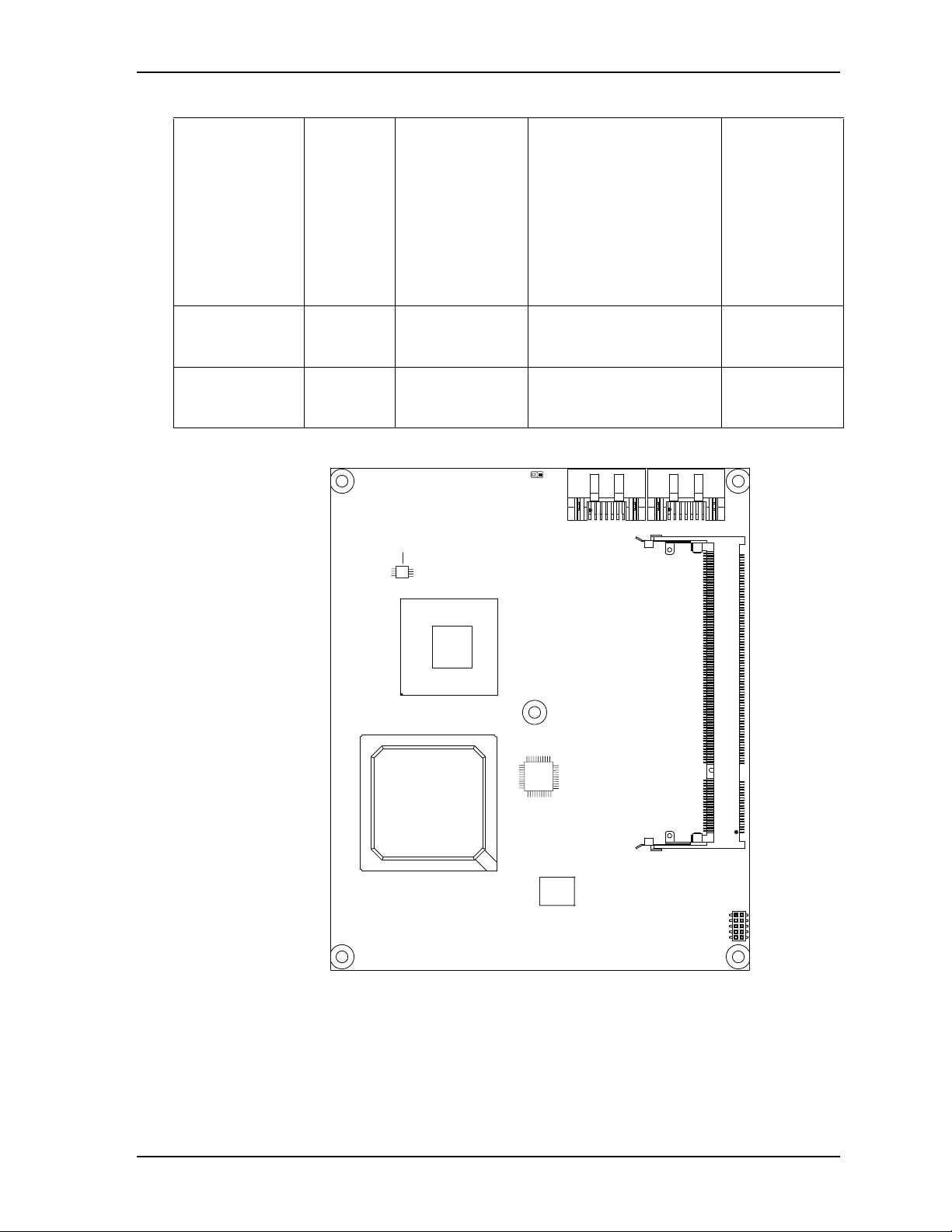
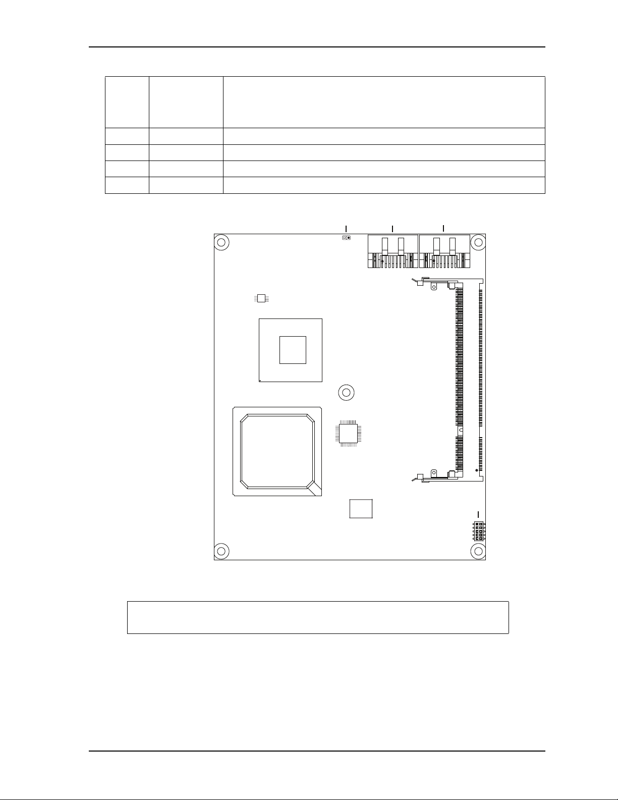
Major Components (ICs)
Table 2 - 1 lists the major ICs, including a brief description of each, on the ETX-PVR. Figures 2-4 and 2-5
show the locations of the ICs.
Table 2-1. Major Components Descriptions and Functions
Chip Type Mfg. Model Description Function
CPU (U1) Intel Atom N455 or
D525
I/O Hub (U2) Intel 82801HBM
(ICH8-M)
PCI-to-ISA
Bridge (U8)
Super I/O
(U9) [See
Figure 2-5 on
page 10.]
HD Audio
CODEC (U11)
[See Figure 2-5
on page 10]
Gigabit Ethernet
PHY Transceiver
(U12)
[See Figure 2-5
on page 10]
SSD (Solid State
Drive, U14) [see
Figure 2-5 on
page 10]
Board Controller
(U19) [see
Figure 2-5 on
page 10]
ITE ITE8888G-L Interface between PCI bus
SMSC SCH3112I-NU Super I/O controller Provides
Realtek ALC262-VD2-GR Encoder and decoder of
Intel 82567V Ethernet PHY transceiver
Greenliant GLS85LP1004P Industrial-grade, soldered
Atmel ATMEGA168 Micro controller for board
1.66GHz, 6.5W (N455) or
1.80GHz, 13W (D525)
processor with 8-way L2
cache
I/O Hub for common user
interfaces
and ISA bus
audio data for transmission,
storage, encryption,
playback, or editing
for 10T/100TX/1000T
Gigabit Ethernet function
solid-state storage module
functions including I²C,
Watchdog Timer, and Power
Button functions
Integrates
Processor Core
and Graphics
Memory
Controller Hub
Provides
Southbridge
interfaces and
off loads some
Northbridge
functions from
the CPU
Migrates legacy
ISA bus
complete legacy
Super I/O
functionality
Provides four
channels of
ADC conversion
and six channels
of DAC display
Provides a
standard IEEE
802.3 Ethernet
interface for
Ethernet transfer
rate up to 1000
Mb/s
Provides solid
state storage
through the IDE
channel
Optimizes power
consumption
versus processor
speed
8 Reference Manual ETX-PVR
Page 15
Chapter 2 Product Overview
Key:
U1 - CPU
U2 - I/O Hub (Southbridge)
U8 - PCI-to-ISA Bridge
U20 - Temperature Sensor
U22 - CPLD
U1
U2
U8
ETX-PVR_Top_Comp_b
U22
U20
Table 2-1. Major Components Descriptions and Functions (Continued)
Temperature
Sensor (U20 - on
bottom side) [see
Figure 2-4 on
page 9]
ON Semi ADT7481ARMZ Digital thermometer and
under/over alarm for local,
CPU, and I/O Hub
temperatures
Measures its
own ambient
temperature and
the temperature
outputs of the
CPU and I/O
Hub. Provides
under/over
temperature
alarm.
CPLD (U22) Xilinx XC9536XL Complex Programmable
Logic Device (not user
programmable)
SPI Flash (U37)
[see Figure 2-5 on
page 10]
PCT PCT25VF016B Serial Peripheral Interface
Flash memory chip
(firmware)
Provides control
for Power
Sequencing
Stores BIOS in
Flash memory
Figure 2-4. Component Locations (Top Side)
ETX-PVR Reference Manual 9
Page 16
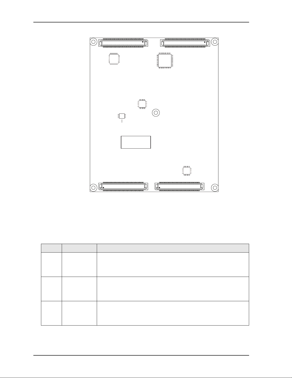
Chapter 2 Product Overview
Key:
U9 - Super I/O
U11 - HD Audio
U12 - Ethernet
U14 - SSD
U19 - Board Controller
U37 - SPI Flash
U14
U9
ETX-PVR_Bottom_Comp_a
U11
U19
U37
U12
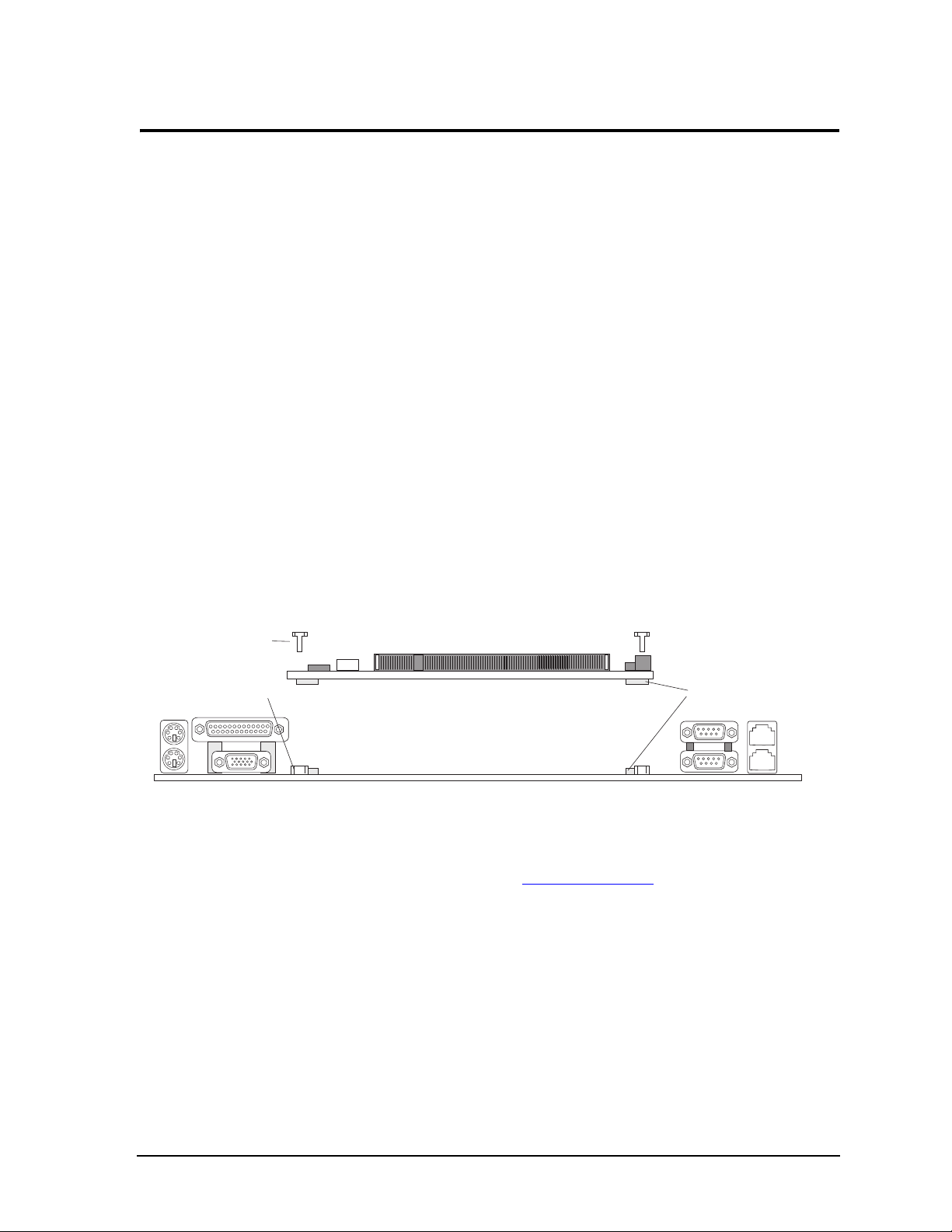
Connector and Socket Definitions
Table 2-2. Connector and Socket Descriptions
Figure 2-5. Component Locations (Bottom Side)
Table 2 - 2 describes the connectors and sockets shown in Figures 2-6 and 2-7.
Jack # Name Description
J1 ETX X1 (on
Standard 100-pin, 0.6 mm Hirose connector for PCI, Audio, and USB signals
bottom side of
the board; see
Figure 2-7.)
J2 ETX X2 (on
back of the
Standard 100-pin, 0.6 mm Hirose connector for ISA signals
board; see
Figure 2-7.)
J3 ETX X3 (on
back of the
Standard 100-pin, 0.6 mm Hirose connector for video, serial, keyboard and
mouse, and parallel/floppy drive signals
board; see
Figure 2-7.)
10 Reference Manual ETX-PVR
Page 17
Chapter 2 Product Overview
Key:
J6 - DDR3 SODIMM socket
J7 - Not supported
J8 - SATA1
J9 - SATA2
JP1 - See jumper table
ETX-PVR_Top_Conn_b
JP1
J6
J7
J8
J9
Table 2-2. Connector and Socket Descriptions (Continued)
J4 ETX X4 (on
back of the
Standard 100-pin, 0.6 mm Hirose connector for IDE, Ethernet, SMBus, I2C,
speaker, VBat, and power management signals
board; see
Figure 2-7.)
J6 SODIMM Standard un-buffered 204-pin socket for DDR3 memory
J7 LPC Not Supported
J8 SATA1 Standard 7-pin, 1.27mm right-angle connector for serial ATA signals
J9 SATA2 Standard 7-pin, 1.27mm right-angle connector for serial ATA signals
Figure 2-6. Connector and Socket Locations (Top Side)
NOTE Pin-1 is shown as a black pin (square or round) in all connectors and jumpers in
all illustrations.
ETX-PVR Reference Manual 11
Page 18
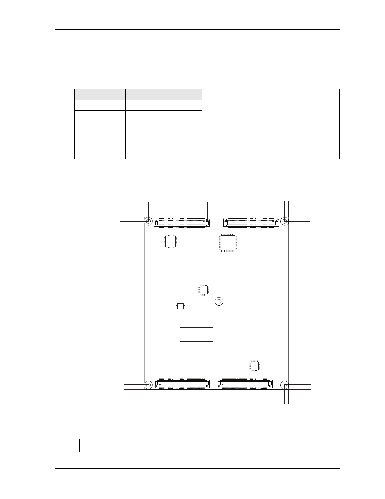
Chapter 2 Product Overview
Key:
J1 - X1 ETX connector
J2 - X2 ETX connector
J3 - X3 ETX connector
J4 - X4 ETX connector
J4 J3
J1
J2
ETX-PVR_Bottom_Conn_a
Jumper Header Definition
Table 2-3. Jumper Header Setting
Figure 2-7. Connector Locations (Bottom Side)
Table 2 - 3 describes the jumper header shown in Figure 2-6 on page 11.
Jumper # Installed Removed/Installed
JP1 – SSD Select (Master/Slave) Master (Default) Slave (Removed)
NOTE Jumpers or shunts use 2mm pitch. A jumper that is removed may be placed on one of
the jumper pins for safe keeping.
12 Reference Manual ETX-PVR
Page 19
Chapter 2 Product Overview
0.00
0.12
4.38
4.26
J4 J3
J1
J2
ETX-PVR_Bottom_Dmn_a
0.00
0.100.10
0.20
2.0
3.55
3.65
0.00
0.36
1.70
3.35
0.12
0.00
4.38
4.26
Specifications
Physical Specifications
Table 2 - 4 provides the physical dimensions of the board.
Table 2-4. Weight and Footprint Dimensions
Item Dimension
Weigh t
Height (overall)
Width
0.10 kg (0.20 lb)
6.35mm (0.25")
95.25mm (3.75")
NOTE Overall height is measured from the
upper board surface to the highest
permanent component on the upper
board surface. This measurement does
not include the cooling solution.
Length
Thickness
Mechanical Specifications
114.3mm (4.5")
2.36mm (0.093")
Figure 2-8. Mechanical Overview (Bottom Side)
NOTE All dimensions are given in inches. Pin 1 is shown as a dot on each ETX connector.
ETX-PVR Reference Manual 13
Page 20

Chapter 2 Product Overview
Environmental Specifications
Table 2 - 5 provides the most efficient operating and storage environmental ranges required for this board.
Table 2-5. Environmental Requirements
Parameter 1.66GHz Atom N455,
1.80GHz Atom D525 CPUs
Environmental Ranges
Operating –20° to +70°C (-4° to +158°F)
Extended
(Optional)
Storage –55° to +85°C (–67° to +185°F)
Temperature
Operating 5% to 90% relative humidity, non-condensing
Non-operating 5% to 95% relative humidity, non-condensing
Humidity
–40° to +85°C (–40° to +185°F)
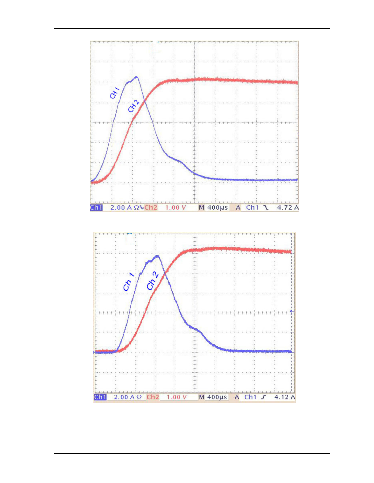
Power Specifications
Table 2 - 6 provides the power requirements for the ETX-PVR.
Table 2-6. Power Supply Requirements
Parameter 1.00GHz N455
Characteristics
(SpeedStep disabled)
Input Type Regulated DC voltages Regulated DC voltages Regulated DC voltages
In-rush Current and
Duration (Typical
Peak)
Idle Current (Typical) 1.71A (8.57W) 1.75A (8.74W) 2.27A (11.37W)
BIT Current (Typical) 2.22A (11.09W) 2.49A (12.46W) 3.31A (16.53W)
S1 Mode 0.25A (1.26W) 0.25A (1.26W) 0.25A (1.26W)
S3 Mode 0.26A (1.29W) 0.26A (1.29W) 0.26A (1.29W)
Note: All test loads include baseboard circuits.
Operating configurations:
See Figure 2-9 See Figure 2-10 See Figure 2-11
1.66GHz N455
Characteristics
1.80GHz D525
Characteristics
• In-rush operating configuration includes video, 2GB DDR3 RAM, one ET1-BBD-R-02 ETX
baseboard, and one AT power supply.
• Idle operating configuration includes the In-rush configuration as well as one SATA hard drive with
Windows XP OS, and PS/2 keyboard and mouse.
• BIT (Burn-In-Test) operating configuration includes the Idle configuration as well as two serial COM
ports with loop backs, one parallel port with loop back, four USB Compact Flash readers each with
256MB of Compact Flash, secondary SATA drive as slave, and one Ethernet connection.
• S1 (Standby) operating configuration is the same as the Idle configuration.
• S3 (Suspend-to-RAM) operating configuration is the same as the Idle configuration.
14 Reference Manual ETX-PVR
Page 21
Chapter 2 Product Overview
Figure 2-9. N455 (with SpeedStep disabled) Peak In-Rush Current and Duration
Figure 2-10. N455 Peak In-Rush Current and Duration
ETX-PVR Reference Manual 15
Page 22
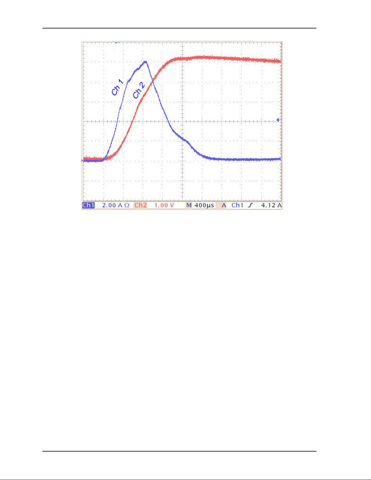
Chapter 2 Product Overview
Figure 2-11. D525 Peak In-Rush Current and Duration
16 Reference Manual ETX-PVR
Page 23

Chapter 2 Product Overview
Heat Spreader
ETX-PVR
COM Board
0.52
ETX
Connector
ETX-PVR_Cooling_Ht_b
ETX-PVR with Heat Spreader
Heat
Sink
ETX-PVR
COM Board
ETX
Connector
2.23
ETX-PVR with Active Heat Sink (Fan)
Heat
Sink
ETX-PVR
COM Board
ETX
Connector
1.56
ETX-PVR with Passive Heat Sink (no Fan)
Thermal/Cooling Requirements
The CPU, I/O Hub, and voltage regulators are the main sources of heat on the board.The ETX-PVR is
designed to operate at the maximum speeds of the N455 (1.66GHz) or N525 (1.80GHz) CPUs and requires
a cooling solution. ADLINK offers two cooling solutions, as well as a heat spreader platform on which to
build a cooling solution (see Table 2-7 for descriptions of the cooling solution options.) Figure 2-12 provides
the height measurements from the bottoms of the ETX connectors to the tops of the cooling components.
NOTE The overall system design must keep the ICs within their operating temperature
specifications.
Table 2-7. ADLINK Optional Cooling Solutions
Cooling Solution Description
Passive Heat Sink
(without fan)
Active Heat Sink
(with fan)
Heat Spreader Provides a simple thermal platform on which to build a cooling solution.
Qualified to maintain optimal performance up to +70°C.
Qualified to maintain optimal performance up to +85°C.
NOTE All heights are given in inches.
Figure 2-12. Stack Heights of Cooling Assemblies
ETX-PVR Reference Manual 17
Page 24

Chapter 2 Product Overview
18 Reference Manual ETX-PVR
Page 25

Chapter 3 Hardware
Overview
This chapter discusses the hardware features of the ETX-PVR in the following order:
• CPU
• Graphics
• Memory
• Interrupt Channel Assignments
• Memory Map
• I/O Address Map
• PCI Bus Interface (J1)
USB
Audio Interface
• ISA Bus Interface (J2 [ISA DMA not supported])
• Primary I/O Interface (J3)
Floppy/Parallel Interface
Serial Port Interfaces
Keyboard
Mouse
Video Interfaces (VGA and LVDS)
• IDE and Auxiliary Interface (J4)
Primary IDE Interface
Ethernet Interface
Power Control and Management
Real Time Clock (RTC)
Speaker
SMBus
• Miscellaneous
Oops! Jumper (BIOS recovery)
Remote Access (Serial Console)
Watchdog Timer (WDT)
Power Interface (including ACPI)
NOTE ADLINK Technology, Inc. only supports the features/options tested and listed in
this manual. The main integrated circuits used in the ETX-PVR may provide
more features or options than are listed for the ETX-PVR, but some of these chip
features or options are not supported on the board and will not function as
specified in the chip documentation.
ETX-PVR Reference Manual 19
Page 26

Chapter 3 Hardware
CPU
The ETX-PVR offers two versions of the Intel Atom™ N400/D500 series CPU—the N455 and
D525—operating at 1.66GHz with 6.5W TDP and 1.80GHz with 13W TDP, respectively. The N400/D500
integrates a low-power and high-performance x86 Processor Core with Memory Controller and 3D Graphics
Engine. This single chip is based on 45-nm, Hi-K process technology, ideal for deeply embedded
applications.
Graphics
The N400/D500 CPU provides a refresh of the Intel third generation graphics core—a 2D/3D graphics
engine that performs pixel shading and vertex shading within a single hardware accelerator, which
minimizes access to memory and improves render performance.
Memory
The ETX-PVR supports one DDR3 SODIMM for up to 2GB of RAM. One 64-bit access channel supports
single- or double-sided DIMMs, allowing for up to two device ranks. Enhanced memory technology on the
board provides optimized bandwidth and reduced latency, increased efficiency of system memory protocol,
and a near continuous data flow to the processor.
20 Reference Manual ETX-PVR
Page 27

Chapter 3 Hardware
Interrupt Channel Assignments (IRQs)
The interrupt channel assignments are listed in Table 3-1.
Table 3-1. Interrupt Channel (IRQs) Assignments (Typical)
Device vs IRQ No. 0 1 2 3 4 5 6 7 8 9 10 11 12 13 14 15
Timer X
Keyboard X
Secondary Cascade X
COM1 O D
COM2 D O
Floppy D
Parallel O D
RTC X
IDE D
Math Coprocessor X
PS/2 Mouse X
HD Audio CODEC D
PCI INTA Automatically Assigned
PCI INTB Automatically Assigned
PCI INTC Automatically Assigned
PCI INTD Automatically Assigned
USB Automatically Assigned
Video Automatically Assigned
Ethernet Automatically Assigned
Legend: D = Default, O = Optional, X = Fixed
NOTE The IRQs for the Ethernet, Video, USB, and PCI are automatically assigned by
the BIOS Plug and Play logic. Local IRQs assigned during initialization can not
be used by external devices.
ETX-PVR Reference Manual 21
Page 28

Chapter 3 Hardware
Memory Map
Table 3 - 2 provides the common PC/AT memory allocations. These are DOS-level addresses. The OS
typically hides these physical addresses by way of memory management.
Table 3-2. Memory Map
Base Address Function
00000000h - 0009FFFFh Conventional Memory
000A0000h - 000AFFFFh Graphics Memory
000B0000h - 000B7FFFh Mono Text Memory
000B8000h - 000BFFFFh Color Text Memory
000C0000h - 000CFFFFh Standard Video BIOS
000D0000h - 000DFFFFh DVMT Memory
000E0000h - 000EFFFFh PCI Express Base Memory
000F0000h - 000FFFFFh System Flash and PCI Resources
I/O Address Map
Table 3 - 3 provides the I/O address map. These are DOS-level addresses. The OS typically hides these
physical addresses by way of memory management.
Table 3-3. I/O Address Map
Address (hex) Subsystem
0000-00F Primary DMA Controller
0020-0021 Master Interrupt Controller
002E-002F SIO Configuration Ports
0040-0043 Programmable Interrupt Timer (Clock/Timer)
0060-006F Keyboard Controller
0070-007F CMOS RAM, NMI Mask Reg, RT Clock
0080-009F DMA Page Registers
00A0-00BF Slave Interrupt Controller
00C0-00DF Slave DMA Controller #2
00F0-00FF Math Coprocessor
01F0-01F8 Primary IDE Hard Disk Controller
0278-027F Parallel Printer
02F8-02FF Serial Port 2 (COM2)
0378-037F Parallel Port (Standard and EPP)
03C0-03DF VGA
03F0-03F7 Floppy Disk Controller
03F8-03FF Serial Port 1 (COM1)
0400-041F SMBus Configuration Ports
0500-053F ICH8 GPIO Configuration Ports
0778-077A Parallel Port (ECP Extensions) (Port 378+400)
0800-087F ICH8 Power Management Ports
22 Reference Manual ETX-PVR
Page 29

Chapter 3 Hardware
Table 3-3. I/O Address Map (Continued)
0A79h ISA PnP Ports
0B00-0B7F SIO Runtime Registers
0CF8-0CFF PCI bus Configuration Address and Data
NOTE 0A79h is the ISA PnP port used by the BIOS and an OS that supports this feature to
recognize ISA PnP (Plug and Play) cards.
The Intel I/O hub ICH-8 (ICH-6 or later) does not support ISA DMA.
X1 PCI Bus Interface (J1)
The J1, 100-pin standard connector is used for the PCI bus, USB ports, and HD Audio interface connections.
This section briefly describes each of these features.
Table 3 - 4 provides the complete pin outs for the J1 (X1) connector.
PCI Bus
The CPU integrates a PCI arbiter that supports up to four external PCI masters.
• Interface carries all of the appropriate PCI signals
• Bus operates at clock speeds up to 33 MHz
• PCI 2.3 Compliant, 32-bit +3.3V PCI interface with +5V tolerant inputs
Universal Serial Bus (USB)
The ETX-PVR module supports up to four USB ports on the baseboard, and the supported features are listed
below.
• USB v2.0 and backwards compatible to Universal UHCI v1.1
• Two root USB hubs and four USB ports
• Supports USB boot of floppy disk drives, hard disk drives, CD-ROMs, or other USB boot devices
• Integrated physical layer transceivers
• Over-current detection status on USB ports 1 and 2
Serial Interrupt Request
This SERIRQ signal is connected to the serial request input on the I/O Hub (ICH8-M) for the alternative
ISA/PCI interrupts. The ETX-PVR SERIRQ pin (pin 21) must be connected to the baseboard to use the ISA
bus on the baseboard.
NOTE The Intel ICH8 I/O Hub does not support ISA DMA.
ETX-PVR Reference Manual 23
Page 30

Chapter 3 Hardware
Audio Interface
The Realtek HD Audio CODEC (ALC262) on the ETX-PVR supports the HDA Link protocol and the
supported features in the following list.
• Supports audio amplifier on baseboard
• PC-Beep pass through to Line Out while reset is held Active Low
• True Line Level Output with volume control independent of Line Out
• Digital 3V and 5V compliant
Tab le 3-4 provides a complete list of the ETX J1 connector signals.
Table 3-4. Complete X1 Interface Pin Signal Descriptions (J1)
J1
Pin
#
1, 2
3 PCICLK3 PCI clock 3 – This signal line is one of four signal lines. These clock signals
4 PCICLK4 PCI clock 4 – Refer to J1, pin-3 for more information.
5, 6
7 PCICLK1 PCI clock 1 – Refer to J1, pin-3 for more information.
8 PCICLK2 PCI clock 2 – Refer to J1, pin-3 for more information.
9 REQ3* Bus Request 3 – This signal line is one of four signal lines. These signals indicate
10 GNT3* Grant 3 – This signal line is one of four signal lines. These signal lines indicate
11 GNT2* Grant 2 – Refer to J1, pin-10 for more information.
12
13 REQ2* Bus Request 2 – This signal line is one of four signal lines. These signals indicate
14 GNT1* Grant 1 – Refer to J1, pin-10 for more information.
15 REQ1* Bus Request 1 – Refer to J1, pin-13 for more information.
16
17 GNT0* Grant 0 – Refer to J1, pin-10 for more information.
18 NC Not Connected (Reserved)
19,
20
21 SERIRQ Serial Interrupt Request – This signal supports the serial interrupt protocol.
22 REQ0* Bus Request 0 – Refer to J1, pin-13 for more information.
23 AD0 Address/Data bus 0 – These signals <AD31 – AD0> are multiplexed on the same
Signal Description
GND Ground
provide the timing outputs for four external PCI devices and the timing for all
transactions on the PCI bus.
GND Ground
to the arbiter that the device desires use of the bus.
access has been granted to the requesting device (PCI Masters).
+3.3V +3.3 volts +/- 5% (Caution: This signal is generated by the ETX-PVR.)
[Note: This signal is not supported on ETX-PVR-R-14, R-16, and R-18 models.]
the device desires use of the bus to the arbiter.
+3.3V +3.3 volts +/- 5% (Caution: This signal is generated by the ETX-PVR.)
[Note: This signal is not supported on ETX-PVR-R-14, R-16, and R-18 models.]
VCC DC Power – +5 volts +/- 5%
PCI connector pins. During the address phase of a PCI cycle, AD31–AD0
contain a 32-bit address or other destination information. During the data phase,
AD31 – AD0 contain data.
24 Reference Manual ETX-PVR
Page 31

Chapter 3 Hardware
Table 3-4. Complete X1 Interface Pin Signal Descriptions (J1) (Continued)
24 +3.3V +3.3 volts +/- 5% (Caution: This signal is generated by the ETX-PVR.)
[Note: This signal is not supported on ETX-PVR-R-14, R-16, and R-18 models.]
25 AD1 Address/Data bus 1 – Refer to J1, pin-23 for more information.
26 AD2 Address/Data bus 2 – Refer to J1, pin-23 for more information.
27 AD4 Address/Data bus 4 – Refer to J1, pin-23 for more information.
28 AD3 Address/Data bus 3 – Refer to J1, pin-23 for more information.
29 AD6 Address/Data bus 6 – Refer to J1, pin-23 for more information.
30 AD5 Address/Data bus 5 – Refer to J1, pin-23 for more information.
31 CBE0* PCI Bus Command/Byte Enable 0 – This signal line is one of four signal lines
multiplexed on the same pins, so that during the address cycle, the command is
defined and during the data cycle, the byte enable is defined.
32 AD7 Address/Data bus 7 – Refer to J1, pin-23 for more information.
33 AD8 Address/Data bus 8 – Refer to J1, pin-23 for more information.
34 AD9 Address/Data bus 9 – Refer to J1, pin-23 for more information.
35,
GND Ground
36
37 AD10 Address/Data bus 10 – Refer to J1, pin-23 for more information.
38 AUXAL Auxiliary A Input Left – This signal is normally used for an external CD-ROM
analog output or similar live-level audio source. Minimum input impedance is 5k
Ohms and nominal input level is 1 volt RMS.
39 AD11 Address/Data bus 11 – Refer to J1, pin-23 for more information.
40 MIC Microphone reference signal – This microphone input signal has a minimum
input impedance of 5k Ohms, and the maximum input voltage is 0.15 V p-p.
41 AD12 Address/Data bus 12 – Refer to J1, pin-23 for more information.
42 AUXAR Auxiliary A Input Right – This signal is normally used for an external CD-ROM
analog output or similar live-level audio source. Minimum input impedance is 5k
Ohms and nominal input level is 1 volt RMS.
43 AD13 Address/Data bus 13 – Refer to J1, pin-23 for more information.
44 NC Not Connected
45 AD14 Address/Data bus 14 – Refer to J1, pin-23 for more information.
46 SNDL Stereo Line Output Left channel – Output signal has a nominal 1 volt RMS level
into 10k impedance load. This output signal can not drive low-impedance
speakers directly.
47 AD15 Address/Data bus 15 – Refer to J1, pin-23 for more information.
48
ASGND Analog Ground – This ground is used for the sound controller and an external
amplifier to achieved the lowest audio noise levels.
49 CBE1* Bus Command and Byte Enable 1 – Refer to J1, pin-31 for more information.
50 SNDR Stereo Line Output Right channel – This output signal has a nominal level of 1
volt RMS into 10k impedance load. This output signal can not drive lowimpedance speakers directly
51,
VCC DC Power – +5 volts +/- 5%
52
53 PAR PCI bus Parity bit – This signal is even parity bit on AD[31:0] and CBE[3:0]*.
54 SERR* System Error – This signal is for reporting address parity errors.
ETX-PVR Reference Manual 25
Page 32

Chapter 3 Hardware
Table 3-4. Complete X1 Interface Pin Signal Descriptions (J1) (Continued)
55 PERR* Parity Error – This signal is driven by the PCI target during a write to indicate a
data parity error has been detected.
56 NC Not connected (Reserved)
57 PME* Power Management Event – This signal is an optional signal that can be used by
a device to request a change in the device or system power state.
58 USB2- Universal Serial Bus Port 2 Data Negative Polarity
59 LOCK* Lock – This signal indicates an operation that may require multiple transactions
to complete.
60 DEVSEL* Device Select – Driven by the target device when its address is decoded.
61 TRDY* Target Ready – This signal indicates the selected device’s ability to complete the
current cycle of transaction. Both IRDY and TRDY must be asserted to
terminate a data cycle.
62 USB3- Universal Serial Bus Port 3 Data Negative Polarity
63 IRDY* Initiator Ready – Indicates the master’s ability to complete the current data cycle.
64 STOP* Stop – Driven by the current PCI target when requesting the master stop the
current transaction.
65 FRAME* PCI bus Frame access – Driven by the current master to indicate the start of a
transaction and will remain active until the final data cycle.
66 USB2+ Universal Serial Bus Port 2 Data Positive Polarity
67,
GND Ground
68
69 AD16 Address/Data bus 16 – Refer to J1, pin-23 for more information.
70 CBE2* Bus Command and Byte Enable 2 – Refer to J1, pin-31 for more information.
71 AD17 Address/Data bus 17 – Refer to J1, pin-23 for more information.
72 USB3+ Universal Serial Bus Port 3 Data Positive Polarity
73 AD19 Address/Data bus 19 – Refer to J1, pin-23 for more information.
74 AD18 Address/Data bus 18 – Refer to J1, pin-23 for more information.
75 AD20 Address/Data bus 20 – Refer to J1, pin-23 for more information.
76 USB0- Universal Serial Bus Port 0 Data Negative Polarity
77 AD22 Address/Data bus 22 – Refer to J1, pin-23 for more information.
78 AD21 Address/Data bus 21 – Refer to J1, pin-23 for more information.
79 AD23 Address/Data bus 23 – Refer to J1, pin-23 for more information.
80 USB1- Universal Serial Bus Port 0 Data Negative Polarity
81 AD24 Address/Data bus 24 – Refer to J1, pin-23 for more information.
82 CBE3* Bus Command and Byte Enable 3 – Refer to J1, pin-31 for more information.
83,
VCC DC Power – +5 volts +/- 5%
84
85 AD25 Address/Data bus 25 – Refer to J1, pin-23 for more information.
86 AD26 Address/Data bus 26 – Refer to J1, pin-23 for more information.
87 AD28 Address/Data bus 28 – Refer to J1, pin-23 for more information.
88 USB0+ Universal Serial Bus Port 0 Data Positive Polarity
89 AD27 Address/Data bus 27 – Refer to J1, pin-23 for more information.
90 AD29 Address/Data bus 29 – Refer to J1, pin-23 for more information.
26 Reference Manual ETX-PVR
Page 33

Chapter 3 Hardware
Table 3-4. Complete X1 Interface Pin Signal Descriptions (J1) (Continued)
91 AD30 Address/Data bus 30 – Refer to J1, pin-23 for more information.
92 USB1+ Universal Serial Bus Port 1 Data Positive Polarity
93 PCIRST* PCI Bus Reset – Signal resets entire PCI Bus. Asserted during a system reset.
94 AD31 Address/Data bus 31 – Refer to J1, pin-23 for more information.
95 INTC* Interrupt C – This signal is used to request an interrupt and only has meaning on
a multi-function device.
96 INTD* Interrupt D – This signal is used to request an interrupt and only has meaning on
a multi-function device.
97 INTA* Interrupt A – This signal is used to request an interrupt.
98 INTB* Interrupt B – This signal is used to request an interrupt and only has meaning on
a multi-function device.
99, 100
Note: The shaded areas denote power or ground. The * symbol indicates the signal is Active Low.
GND Ground
X2 ISA Bus Interface (J2)
The J2, 100-pin connector is used for standard ISA interface connections. The CPU does not directly support
an ISA expansion interface. A provision for ISA bus capabilities is provided in this connector through an onboard PCI-to-ISA bridge. Refer to Table 3-5 for pin definitions of the X2 interface.
Table 3-5. Complete X2 ISA Bus Interface Pin Signal Descriptions (J2)
J2
Pin #
1, 2
3 SD14 System Data 14 – These signals (0 to 19) provide system data bits.
4 SD15 System Data 15 – Refer to SD14, pin-3 for more information.
5 SD13 System Data 13 – Refer to SD14, pin-3 for more information.
6 MASTER* Bus Master – This signal is used by an ISA board to gain ownership of the ISA
7 SD12 System Data 12 – Refer to SD14, pin-3 for more information.
8 NS Not Supported
9 SD11 System Data 11 – Refer to SD14, pin-3 for more information.
10 NS Not Supported
11 SD10 System Data 10 – Refer to SD14, pin-3 for more information.
12 NS Not Supported
13 SD9 System Data 9 – Refer to SD14, pin-3 for more information.
14 NS Not Supported
15 SD8 System Data 8 – Refer to SD14, pin-3 for more information.
16 NS Not Supported
17 MEMW* Memory Write – This signal instructs a selected memory device to store data
18 NS Not Supported
Signal Description
GND Ground
bus.
currently on the data bus. It is active on all memory write cycles.
ETX-PVR Reference Manual 27
Page 34

Chapter 3 Hardware
Table 3-5. Complete X2 ISA Bus Interface Pin Signal Descriptions (J2) (Continued)
19 MEMR* Memory Read – This signal instructs a selected memory device to drive data
onto the data bus. It is active on all memory read cycles.
20 NS Not Supported
21 LA17 Latchable Address 17 – These signals (0-23) must be latched by the resource if
the line is required for the entire data cycle.
22 NS Not Supported
23 LA18 Latchable Address 18 – Refer to LA17, pin-21 for more information.
24 IRQ14 Interrupt Request 14 – Asserted by a device when it has pending interrupt
request. Only one device may use the request line at a time.
25 LA19 Latchable Address 19 – Refer to LA17, pin-21 for more information.
26 IRQ15 Interrupt Request 15 – Asserted by a device when it has pending interrupt
request. Only one device may use the request line at a time.
27 LA20 Latchable Address 20 – Refer to LA17, pin-21 for more information.
28 IRQ12 Interrupt Request 12 – Asserted by a device when it has pending interrupt
request. Only one device may use the request line at a time.
29 LA21 Latchable Address 21– Refer to LA17, pin-21 for more information.
30 IRQ11 Interrupt Request 11 – Asserted by a device when it has pending interrupt
request. Only one device may use the request line at a time.
31 LA22 Latchable Address 22 – Refer to LA17, pin-21 for more information.
32 IRQ10 Interrupt Request 10 – Asserted by a device when it has pending interrupt
request. Only one device may use the request line at a time.
33 LA23 Latchable Address 23 – Refer to LA17, pin-21 for more information.
34 IO16* I/O Chip Select 16 – This signal is driven low by an I/O slave device to indicate
it is capable of performing a 16-bit I/O data transfer. This signal is driven from
a decode of the SA15 to SA0 address lines.
35, 36
GND Ground
37 SBHE* System Byte High Enable – This signal is driven low to indicate a transfer of
data on the high half of the data bus (D15 to D8).
38 M16* Memory Chip Select 16 – This signal is driven low by a memory slave device to
indicates it is cable of performing a 16-bit memory data transfer. This signal is
driven from a decode of the LA23 to LA17 address lines.
39 SA0 System Address 0 – These signals (0 to 19) provide system address bits.
40 OSC Oscillator – This clock signal operates at 14.3 MHz. This signal is not
synchronous with the system clock (SYSCLK).
41 SA1 System Address 1– Refer to SA0, pin-39 for more information.
42 BALE Buffered Address Latch Enable – This signal is used to latch the LA23 to LA17
signals or decodes of these signals. Addresses are latched on the falling edge of
BALE.
43 SA2 System Address 2 – Refer to SA0, pin-39 for more information.
44 NS Not Supported
45 SA3 System Address 3 – Refer to SA0, pin-39 for more information.
46 NS Not Supported
47 SA4 System Address 4 – Refer to SA0, pin-39 for more information.
48 IRQ3 Interrupt Request 3 – Asserted by a device when it has pending interrupt
request. Only one device may use the request line at a time.
28 Reference Manual ETX-PVR
Page 35

Chapter 3 Hardware
Table 3-5. Complete X2 ISA Bus Interface Pin Signal Descriptions (J2) (Continued)
49 SA5 System Address 5 – Refer to SA0, pin-39 for more information.
50 IRQ4 Interrupt Request 4 – Asserted by a device when it has pending interrupt
request. Only one device may use the request line at a time.
51, 52
VCC DC Power – +5 volts +/- 5%
53 SA6 System Address 6 – Refer to SA0, pin-39 for more information.
54 IRQ5 Interrupt Request 5 – Asserted by a device when it has pending interrupt
request. Only one device may use the request line at a time.
55 SA7 System Address 7 – Refer to SA0, pin-39 for more information.
56 IRQ6 Interrupt Request 6 – Asserted by a device when it has pending interrupt
request. Only one device may use the request line at a time.
57 SA8 System Address 8 – Refer to SA0, pin-39 for more information.
58 IRQ7 Interrupt Request 7 – Asserted by a device when it has pending interrupt
request. Only one device may use the request line at a time.
59 SA9 System Address 9 – Refer to SA0, pin-39 for more information.
60 SYSCLK System Clock – This is a free running clock typically in the 8 MHz to 10 MHz
range, although its exact frequency is not guaranteed.
61 SA10 System Address 10 – Refer to SA0, pin-39 for more information.
62 REFSH* Memory Refresh – This signal is driven low to indicate a memory refresh cycle
is in progress. Memory is refreshed every 15.6 usec.
63 SA11 System Address 11 – Refer to SA0, pin-39 for more information.
64 NS Not Supported
65 SA12 System Address 12 – Refer to SA0, pin-39 for more information.
66 NS Not Supported
67, 68
GND Ground
69 SA13 System Address 13 – Refer to SA0, pin-39 for more information.
70 NS Not Supported
71 SA14 System Address 14 – Refer to SA0, pin-39 for more information.
72 NS Not Supported
73 SA15 System Address 15 – Refer to SA0, pin-39 for more information.
74 IOR* I/O Read – This strobe signal is driven by the owner of the bus (ISA bus master)
and instructs the selected I/O device to drive read data onto the data bus.
75 SA16 System Address 16 – Refer to SA0, pin-39 for more information.
76 IOW* I/O Write – This strobe signal is driven by the owner of the bus (ISA bus
master) and instructs the selected I/O device to capture the write data on the
data bus.
77 SA18 System Address 18 – Refer to SA0, pin-39 for more information.
78 SA17 System Address 17 – Refer to SA0, pin-39 for more information.
79 SA19 System Address 19 – Refer to SA0, pin-39 for more information.
80 SMEMR* System Memory Read – This signal is used by bus owner to request a memory
device to drive data onto the data bus and only active for lower 1 MB. Used for
legacy compatibility with 8-bit cards.
ETX-PVR Reference Manual 29
Page 36

Chapter 3 Hardware
Table 3-5. Complete X2 ISA Bus Interface Pin Signal Descriptions (J2) (Continued)
81 IOCHRDY I/O Channel Ready – This signal allows slower ISA boards to lengthen I/O or
memory cycles by inserting wait states. This signal’s normal state is active high
(ready). ISA boards drive the signal inactive low (not ready) to insert wait
states. Devices using this signal to insert wait states should drive it low
immediately after detecting a valid address decode and an active read, or write
command. The signal is released high when the device is ready to complete the
cycle.
82 NS Not Supported
83, 84
VCC DC Power – +5 volts +/- 5%
85 SD0 System Data 0 – Refer to SD14, pin-3 for more information.
86 SMEMW* System Memory Write – This signal is used by bus owner to request a memory
device to store data currently on the data bus and only active for the lower
1 MB. Used for legacy compatibility with 8-bit cards.
87 SD2 System Data 2 – Refer to SD14, pin-3 for more information.
88 SD1 System Data 1 – Refer to SD14, pin-3 for more information.
89 SD3 System Data 3 – Refer to SD14, pin-3 for more information.
90 NOWS* No Wait State – This signal is driven low by a bus slave device to indicate it is
capable of performing a bus cycle without inserting any additional wait states.
To perform a 16-bit memory cycle without wait states, this signal is derived
from an address decode.
91 NS Not Supported
92 SD4 System Data 4 – Refer to SD14, pin-3 for more information.
93 SD5 System Data 5 – Refer to SD14, pin-3 for more information.
94 IRQ9 Interrupt Request 9 – Asserted by a device when it has pending interrupt
request. Only one device may use the request line at a time.
95 SD6 System Data 6 – Refer to SD14, pin-3 for more information.
96 SD7 System Data 7 – Refer to SD14, pin-3 for more information.
97 IOCHK* I/O Channel Check – This signal may be activated by ISA boards to request that
a non-maskable interrupt (NMI) be generated to the system processor. It is
driven active to indicate an uncorrectable error has been detected.
98 RSTDRV Reset Drive – This signal is used to reset or initialize system logic on power up
or subsequent system reset.
99
100
GND Ground
GND Ground
Note: The shaded areas denote power or ground. The * symbol indicates the signal is Active Low.
30 Reference Manual ETX-PVR
Page 37

Chapter 3 Hardware
X3 Primary I/O Interface (J3)
The J3, 100-pin connector is used for Floppy or Printer (LPT1) interface, Serial interfaces (COM1 and
COM2), Mouse and Keyboard interfaces, and the video interfaces for standard VGA and LVDS video. This
section briefly describes each of these features. Refer to Table 3-6 on page 32 for pin definitions of the X3
interface.
Floppy Interface
The Floppy interface shares signal lines with the Parallel interface and is provided by the Super I/O chip
(SCH3112I-NU). The BIOS settings determine which one is operational.
• Supports two floppy drives
• Supports 16 bytes of FIFO with data rates up to 1 Mbps
Parallel Interface
Parallel interface supports standard parallel, Bi-directional, ECP and EPP protocols. The Super I/O chip
(SCH3112I-NU) provides the parallel interface signals, which are shared with the floppy drive interface.
• Shares signal lines with the Floppy interface, and the BIOS settings determine which one is operational
• Supports Standard Printer Port (SPP), Enhanced Parallel Port (EPP) and Enhanced Capabilities Port
(ECP)
Serial Ports 1 and 2
The Super I/O chip (SCH3112I-NU) provides the circuitry for two serial port UARTs. The signals for serial
ports 1 and 2 are provided to the baseboard through connector J3. However, the baseboard must provide the
serial transceivers to make use of this feature. The serial port features are:
• Two individual 16550-compatible UARTs
• Programmable word length, stop bits and parity
• 16-bit programmable baud rate generator and Interrupt generator
• Loop-back mode
• Two individual 16-bit FIFOs
PS/2 Keyboard
The signal lines for a PS/2 keyboard are provided through the J3 connector from the Super I/O chip
(SCH3112I-NU).
PS/2 Mouse
The signal lines for a PS/2 mouse are provided through the J3 connector from the Super I/O chip
(SCH3112I-NU).
VGA Interface
The N455 version of the CPU provides direct VGA outputs with a resolution up to 1400x1050 @ 60Hz. The
D525 version of the CPU provides resolutions up to 2048x1536 @ 60Hz.
The analog display output provides an RGB signal output as well as an HSYNC and a VSYNC signal. The
display function contains a RAM-based Digital-to-Analog Converter (RAMDAC) that transforms the digital
data from the graphics and video subsystems to analog data for CRT monitors.
ETX-PVR Reference Manual 31
Page 38

Chapter 3 Hardware
LVDS Interface
The CPU provides direct LVDS outputs, which support a single channel 18-bit LVDS interface with three
signal lines. The N455 CPU provides digital LVDS resolution up to 1280x800, and the D525 CPU provides
resolutions up to 1366x768.
NOTE The necessary voltages to drive a flat panel are not supplied through the J3 connector
on the ETX-PVR module. The required drive voltages for the flat panel must be
designed into the customer’s baseboard and supplied from the ATX or AT power
supply to provide drive voltages for the LVDS connector to the flat panel.
Table 3 - 6 describes the pin signals of the X3 ETX interface connector.
Table 3-6. Complete X3 Interface Pin Signal Descriptions (J3)
J3
Pin #
1, 2
3 Red Red – This is the Red analog output signal to the CRT.
4 Blue Blue – This is the Blue analog output signal to the CRT.
5 HSYNC Horizontal Sync – This signal is used for the digital horizontal sync output
6 Green Green – This is the Green analog output signal to the CRT.
7 VSYNC Vertical Sync – This signal is used for the digital vertical sync output to the
8 DDCK Display Data Channel Clock – This signal line provides the data clock signal
9 NC Not Connected
10 DDDA Display Data Channel Data – This signal line provides information to the
11 NC Not Connected
12 NC Not Connected
13 NC Not Connected
14 NC Not Connected
15, 16
17 NC Not Connected
18 NC Not Connected
19 NC Not Connected
20 NC Not Connected
21, 22
23 NC Not Connected
24 NC Not Connected
25 NC Not Connected
26 NC Not Connected
27, 28
Signal Description
GND Ground
to the CRT.
CRT.
to the Memory Hub from the monitor. This is part of the Plug and Play
standard developed by the VESA trade association.
Memory Hub about the monitor type, brand, model. This is part of the Plug
and Play standard developed by the VESA trade association.
GND Ground
GND Ground
GND Ground
32 Reference Manual ETX-PVR
Page 39

Chapter 3 Hardware
Table 3-6. Complete X3 Interface Pin Signal Descriptions (J3) (Continued)
29 LCDDO4 Data Negative Output, Line 2, Channel 1
30 LCDDO7 Clock Positive Output, Clock, Channel 1
31 LCDDO5 Data Positive Output, Line 2, Channel 1
32 LCDDO6 Clock Negative Output, Clock, Channel 1
33, 34
GND Ground
35 LCDDO1 Data Positive Output, Line 0, Channel 1
36 LCDDO3 Data Positive Output, Line 1, Channel 1
37 LCDDO0 Data Negative Output, Line 0, Channel 1
38 LCDDO2 Data Negative Output, Line 1, Channel 1
39, 40
41 JILI_DAT
VCC DC Power – +5V +/- 5%
2
Flat Panel I
C Data – This is the I2C data interface to the parameter
EEPROM used with the flat panel.
42 LTGIO0 General Purpose I/O
43 JILI_CLK
Flat Panel I
2
C Clock – This is the I2C clock interface to the parameter
EEPROM used with the flat panel.
44 BLON* Backlight On – This signal controls the external backlight power for the flat
panel.
45 BIASON
BIAS ON – This signal controls the flat panel contrast voltage.
(DNP)
46 DIGON Digital Power On – This signal controls the digital flat panel power up.
47 NC Not Connected
48 NC Not Connected
49 NC Not Connected
50 NC Not Connected
51 LPT/FLPY* Parallel/Floppy Select – This signal selects the parallel or floppy port
signals. If this signal is Low at boot time, the floppy drive is selected. If this
signal is High at boot time, the parallel port is selected. This state can not be
changed until the next boot cycle.
52 NC Not Connected (Reserved)
53
VCC DC Power – +5 volts +/- 5%
54 GND Ground
55 Strobe*
Parallel Strobe – This output signal is used to strobe data into the printer. I/O
pin in ECP/EPP mode.
DS0*
56 AFD*
Floppy Drive Select 0 – Selects drive 0.
Parallel Auto Feed – This is a output signal from the printer to
automatically feed one line after each line is printed.
DENSEL
Floppy Drive Density Select – This signal indicates if a low (250/300 kbps)
or high (500/1 kbps) data rate is selected.
57 NC Not Connected (Reserved)
58 PD7 Parallel Port Data 7 – This signal (0 to 7) provides a parallel port data signal
and is the printer data MSB.
59 NS Not Supported
ETX-PVR Reference Manual 33
Page 40

Chapter 3 Hardware
Table 3-6. Complete X3 Interface Pin Signal Descriptions (J3) (Continued)
60 ERR*
Parallel Error – This is a status output signal from the printer. A low state
indicates an error condition on the printer.
HDSEL*
Floppy Head Select – Selects floppy diskette side for Read/Write operations
(0 = side 1, 1 = side 0).
61 NS Not Supported
62 PD6
MTR0*
Parallel Port Data 6 – Refer to pin-58 and 80 for more information.
Floppy Motor Control 0 – Select motor on drive 0.
63 RXD2 Receive Data 2 – Serial port 2 receive data in.
64 INIT*
Parallel Initialize – This signal initializes the printer. Output in standard
mode, I/O in ECP/EPP mode.
DIR*
Floppy Direction – Direction of head movement (0 = inward motion,
1 = outward motion).
65, 66
GND Ground
67 RTS2* Request To Send 2 – Indicates Serial port 2 is ready to transmit data. Used as
hardware handshake with CTS2 for low level flow control.
68 PD5 Parallel Port Data 5 – Refer to pin-58 and 80 for more information.
69 DTR2* Data Terminal Ready 2 – Indicates Serial port 2 is powered, initialized, and
ready. Used as hardware handshake with DSR2 for overall readiness.
70 SLCTIN
Parallel Select In – This output signal is used to select the printer. I/O pin in
ECP/EPP mode.
STEP*
Floppy Step – Low pulse for each track-to-track movement of the head.
71 DCD2* Data Carrier Detect 2 – Indicates external serial device is detecting a carrier
signal (i.e., a communication channel is currently open). In direct connect
environments, this input is driven by DTR2 as part of the DTR2/DSR2
handshake.
72 PD4
Parallel Port Data 4 – Refer to pin-58 and 80 for more information.
DSKCHG*
Floppy Disk Change – Senses the drive door is open or the diskette has been
changed since the last drive selection.
73 DSR2* Data Set Ready 2 – Indicates external serial device is powered, initialized,
and ready. Used as hardware handshake with DTR2 for overall readiness.
74 PD3
RDATA*
Parallel Port Data 3 – Refer to pin-58 and 80 for more information.
Floppy Read Data – Raw serial bit stream from drive for read operations.
75 CTS2* Clear To Send 2 – Indicates external serial device is ready to receive data.
Used as hardware handshake with RTS2 for low level flow control.
76 PD2
WPT*
Parallel Port Data 2 – Refer to pin-58 and 80 for more information.
Floppy Write Protect – Senses the diskette is write protected.
77 TXD2 Transmit Data 2 – Serial port 2 transmit data out.
78 PD1
TRK0*
Parallel Port Data 1 – Refer to pin-58 and 80 for more information.
Floppy Track 0 – Sensor detects when head is positioned over track 0.
79 RI2* Ring Indicator 2 – Indicates external serial device is detecting a ring
condition. Used by software to initiate operations to answer and open the
communications channel.
34 Reference Manual ETX-PVR
Page 41

Chapter 3 Hardware
Table 3-6. Complete X3 Interface Pin Signal Descriptions (J3) (Continued)
80 PD0
Parallel Port Data 0 – This pin (0 to 7) provides a parallel port data signal
and is the printer data LSB.
INDEX*
Floppy Index – Sense to detect that the head is positioned over the beginning
of a track.
81, 82
VCC +5 volts +/- 5%
83 RXD1 Receive Data 1 – Serial port 1 receive data in.
84 ACK*
Parallel Acknowledge – This is a status input signal from the printer. A Low
State indicates it has received the data and is ready to accept new data.
DR1
Floppy Drive Select 1 – This signal selects drive 1.
85 RTS1* Request To Send 1 – Indicates Serial port 1 is ready to transmit data. Used as
hardware handshake with CTS1 for low level flow control.
86 BUSY
Parallel Busy – This is a status input signal from the printer. A high state
indicates the printer is not ready to accept data.
MTR1
Floppy Motor Control 1 – This signal selects motor on drive 1.
87 DTR1* Data Terminal Ready 1 – Indicates Serial port 1 is powered, initialized, and
ready. Used as hardware handshake with DSR1 for overall readiness.
88 PE
Parallel Paper End – This is a status input signal from the printer. A high
state indicates it is out of paper.
WDATA*
Floppy Write Data – Sends encoded data to drive for write operations.
89 DCD1* Data Carrier Detect 1 – Indicates external serial device is detecting a carrier
signal (i.e., a communication channel is currently open). In direct connect
environments, this input is driven by DTR1 as part of the DTR1/DSR1
handshake.
90 SLCT
Parallel Select – This is a status output signal from the printer. A high state
indicates it is selected and powered on.
WGATE*
Floppy Write Enable – Signal enables current flow in drive write head.
91 DSR1* Data Set Ready 1 – Indicates external serial device is powered, initialized,
and ready. Used as hardware handshake with DTR1 for overall readiness.
92 MSCLK Mouse Clock signal – This signal clocks the data from the mouse.
93 CTS1* Clear To Send 1 – Indicates external serial device is ready to receive data.
Used as hardware handshake with RTS1 for low level flow control.
94 MSDAT Mouse Data signal – This signal provides the mouse data.
95 TXD1 Transmit Data 1 – Serial port 1 transmit data out.
96 KBCLK Keyboard Clock signal – This signal clocks the data from the keyboard.
97 RI1* Ring Indicator 1 – Indicates external serial device is detecting a ring
condition. Used by software to initiate operations to answer and open the
communications channel.
98 KBDAT Keyboard Data signal – This signal provides the keyboard data.
99
100
GND Ground
GND Ground
Note: The shaded areas denote power or ground. The * symbol indicates the signal is Active Low.
ETX-PVR Reference Manual 35
Page 42

Chapter 3 Hardware
X4 IDE and Auxiliary Interface (J4)
The J4, 100-pin connector is used for the IDE port, Ethernet port, RTC/Battery, speaker, power management,
SMBus, I2C bus, and miscellaneous power interface signals. This section describes each of these features.
Refer to Table 3-8 on page 38 for pin definitions of the X4 interface.
IDE Port
• Supports one EIDE channel for the on-board Solid State Drive (SSD) and up to two devices
• Supports EIDE Ultra DMA 33/66/100 in Master Mode
• Supports PIO IDE transfers up to 14 Mbytes/sec
• Supports IDE Bus Master transfers up to 100 Mbytes/sec
Ethernet Port Interface
The ICH8-M integrates one Gigabit Ethernet (GbE) controller. The integrated GbE controller delivers
signals to the Intel 82567V Gigabit Ethernet transceiver, which offers physical layer (PHY) signals to the
ETX X4 interface. The ETX specification supports only a 10/100 fast Ethernet solution and therefore
utilizes only the first MDI pair (MDI1 and MDI2). Refer to the following bullets for a list of the Ethernet
port features.
• Supports low power 3.3V device
• Provides chained memory structure
• Supports full duplex or half-duplex operation
• Supports full duplex operation at 10 Mbps and 100 Mbps
• Supports half-duplex mode with enhanced performance by a proprietary collision reduction mechanism
• Provides IEEE 802.3 10BaseT/100BaseTX compatible physical layer
• Supports data transmission with minimum interframe spacing (IFS)
• Supports IEEE 802.3u Auto-Negotiation
• Provides 3 KB transmit and 3 KB receive FIFOs (helps prevent data underflow and overflow)
• Provides IEEE 802.3x 100BaseTX flow control
• Improved dynamic transmit chaining with multiple priorities transmit queues
• Supports an Ethernet port RJ-45 connector and the magnetics on the baseboard only
36 Reference Manual ETX-PVR
Page 43

Chapter 3 Hardware
Power Control Signals
The ETX-PVR supports various power control signals provided through the baseboard to control the
ETX-PVR and the power supply.
• The Power Good input signal (PWGIN) is provided from an external input typically from the external
power supply (ATX) to the baseboard. This signal is typically an active-high input to the ETX
baseboard and indicates to the ETX module it can begin the boot process. This Power Good signal can
also be used as an active-low reset input to the ETX module.
• The Power Suspend signal (5V_SB) must be provided through the power supply interface for standby
operation, typically an ATX power supply. The power supply must provide a 5 volt
130mA stand-by power source for this function to be available.
• The Power On signal (PS_ON) is provided by the ETX module to the PS_ON input of an ATX power
supply allowing it to switch to main output power from a standby state. This signal is used in
conjunction with the 5V_SB supplied to the ETX module from the ATX power supply.
• The Power Button Input signal (PWRBTN*) provides a ground temporally through a momentary-
contact switch or through an open collector driver to the ATX power supply. This signal is used in
conjunction with the PS_ON and the 5V_SB signals from the ATX power supply to activate the power
control function of the power supply.
• A voltage monitor on the ETX-PVR tracks the VCC voltage (+5 volts) state by monitoring the +3.3V
generated on the ETX module. When the +3.3V drops below 3.0V or the Reset Button signal goes low,
the voltage monitor sends a reset pulse to the CPU and the I/O Hub.
* indicates Active Low.
Power Management Signals
The ETX-PVR supports various power management signals described in the following list.
• The External System Management Interrupt (EXTSMI) signal is routed to the baseboard through J4 to
allow external circuitry to initiate an SMI for the ETX module.
• The Resume Reset input (RSMRST*) signal to the ETX module may be driven low by external control
circuitry to reset the power management logic on the ETX module.
• The System Management Bus Alert input (SMBALRT*) signal is used by SMBus devices to indicate an
event on the SMBus to the ETX module.
• The Battery Low input (BATLOW*) signal is used by external voltage monitoring circuitry to indicate
the system battery is low to the ETX module.
* indicates Active Low.
Speaker
The signal lines for a speaker port with 0.1-watt drive are provided through the J4 connector to the
baseboard where the speaker must be located.
The I/O Hub provides the speaker output signal, but the output drive circuit must be implemented on the
baseboard.
Real Time Clock (RTC)
The ETX-PVR supports a Real Time Clock (RTC) and CMOS RAM for the BIOS Setup Utility. The RTC
and 256 byte of CMOS RAM are included inside the I/O Hub. The RTC and CMOS are backed up through
the BAT pin on J4 with a battery located on the baseboard. If the battery is not present, the BIOS has a
battery-free boot option to complete the boot process.
ETX-PVR Reference Manual 37
Page 44

Chapter 3 Hardware
SMBus
The I/O Hub contains an integrated SMBus controller with both a host and slave SMBus port; but the host
cannot access the slave internally. The slave port allows an external master access to the I/O Hub through the
J4 connector. The master contained in the I/O Hub is used to communicate with the SODIMM SPD (Serial
Presence Detect), Temperature Sensor, and the clock generator. Ta ble 3 -7 lists the addresses for these
devices with the components and corresponding binary addresses of the SMBus.
Table 3-7. SMBus Reserved Addresses
Matrix Component Address Binary
SODIMM SPD 1010,000x
Clock Generator 1101,001x
Temperature Sensor 1001,100x
Table 3 - 8 describes the pin signals of the ETX-PVR X4 ETX interface connector.
Table 3-8. Complete X4 Interface Pin Signal Descriptions (J4)
b
b
b
J4
Signal Description
Pin
#
1, 2
GND Ground
3 5V_SB 5 volt Suspend – This control signal is sent to the ATX power supply for a
suspended or standby state.
4PWGIN
Power Good In – This active high input signal indicates to the ETX-PVR the
power is good, and it can begin the boot process.
5 PS_ON Power Supply On – This active low output signal from the ETX-PVR is sent
to the ATX power supply to turn it on.
6 SPEAKER Speaker – This PC speaker output signal must be connected to a speaker
(piezoelectric or dynamic) on the baseboard to hear the output (beeps).
7 PWRBTN* Power Button – This signal provides a ground temporally through an open
collector driver to the ATX power supply to change states (turn it on).
8 BATT Battery Voltage – This is the + battery connection to baseboard for +3 volt
lithium backup battery used for RTC operation and CMOS non-volatile
memory.
9 NC Not Connected
10 LILED Link Integrity LED – The LINK LED pin indicates link integrity. If the link is
valid in either 10 or 100Mbps, the LED is on; if the link is invalid, the LED is
off.
11 RSMRST* Resume Reset – This signal is driven low by external circuitry to reset the
power management logic on the ETX-PVR.
12 ACTLED Activity LED – The Activity LED pin indicates either transmit or receive
activity. When activity is present, the activity LED is on; when no activity is
present, the activity LED is off.
13 NC Not Connected
14 SPDLED Speed LED – The speed LED pin indicates the speed. The speed LED will be
on at 100 Mbps and off at 10 Mbps.
15 NC Not Connected
16
2
I
CLK This clock line implements an I2C bus, which supports external slave devices
only. The I
2
C interface supports EEPROMs and other simple I/O devices.
38 Reference Manual ETX-PVR
Page 45

Chapter 3 Hardware
Table 3-8. Complete X4 Interface Pin Signal Descriptions (J4) (Continued)
17, 18VCC DC Power – +5 volts +/-5%
19 OVCR* Over Current Detect – This signal indicates a USB over-current condition.
20 NC Not Connected
21 EXTSMI* External System Management Interrupt – This signal is provided by external
circuitry to initiate an SMI event with the ETX-PVR.
22
2
I
DAT This data line implements an I2C bus, which supports external slave devices
2
only. The I
C interface supports EEPROMs and other simple I/O devices.
23 SMBCLK System Management Bus Clock – This signal is used to support internal and
external SMBus devices, such as temperature and battery monitoring.
24 SMBDATA System Management Bus Data – This signal is used to support internal and
external SMBus devices, such as temperature and battery monitoring.
25 NC Not Connected
26 SMBALRT* System Management Bus Alert – This signal is used by SMBus devices to
signal an event on the SMBus.
27 NC Not Connected
28 DASP* Drive Active/Drive Present – This signal is time-multiplexed and indicates
the drive is present and active. If a Compact Flash is connected to the
baseboard, this signal must be routed to the DASP pin of any other device
connected to the IDE channel. May also be used for Master/Slave negotiation
on the IDE channel.
29 NC Not Connected
30 PIDE_CS3* Primary Chip Select 1 – Selects host-accessible Command Block Register.
31 NC Not Connected
32 PIDE_CS1* Primary Chip Select 0 – Selects host-accessible Command Block Register.
33,
GND Ground
34
35 PDIAG Passed Diagnostics – This signal is used for Master/Slave negotiation on the
IDE channel. It is asserted by the Slave to indicate to master that the slave has
passed its internal Diagnostics command. If a Compact Flash is connected to
the baseboard, this signal must be routed to the DASP pin of any another
device connected to the IDE channel.
May also be used to detect the presence of an 80-conductor IDE cable, which
is required for support of the DMA66 or DMA100 high-speed transfers.
36 PIDE_A2 Primary Drive Address Bus 2 – Used <0 to 2> to indicate which byte in the
ATA command block or control block (register) is being accessed.
37 NC Not Connected
38 PIDE_A0 Primary Drive Address Bus 0 – Refer to J4, pin-36, for more information.
39 NC Not Connected
40 PIDE_A1 Primary Drive Address Bus 1 – Refer to J4, pin-36, for more information.
41 BATLOW* Battery Low – This external signal to the ETX-PVR indicates when the
external battery is low.
42 NC Not Connected
43 NC Not Connected
ETX-PVR Reference Manual 39
Page 46

Chapter 3 Hardware
Table 3-8. Complete X4 Interface Pin Signal Descriptions (J4) (Continued)
44 PIDE_INTRQ Primary Drive Interrupt Request (IRQ 14) – Asserted by drive when it has
pending interrupt (PIO transfer of data to or from the drive to the host).
45 NC Not Connected
46 PIDE_AK* Primary DMA Channel Acknowledge – Used by the host to acknowledge
data has been accepted or data is available. Used in response to
PIDE_DMARQ when asserted.
47 NC Not Connected
48 PIDE_RDY Primary I/O Channel Ready – When negated extends the host transfer cycle
of any host register access when the drive is not ready to respond to a data
transfer request. High impedance if asserted.
49,
VCC DC Power – +5 volts +/-5%
50
51 NC Not Connected
52 PIDE_IOR* Primary Drive I/O Read – Primary strobe signal for read functions. Negative
edge enables data from a register or data port of the drive onto the host data
bus. Positive edge latches data at the host.
53 NC Not Connected
54 PIDE_IOW* Primary Drive I/O Write – Primary strobe signal for write functions. Negative
edge enables data from a register or data port of the drive onto the host data
bus. Positive edge latches data at the host.
55 NC Not Connected
56 PIDE_DRQ Primary DMA Request – Used for DMA transfers between host and drive
(direction of transfer controlled by IOR* and IOW*). Also used in an
asynchronous mode with ACK*. Drive asserts an IRQ when ready to transfer
or receive data.
57 NC Not Connected
58 PIDE_D15 Primary Disk Data 15 – These signals (0 to 15) provide the Primary IDE disk
data signals.
59 NC Not Connected
60 PIDE_D0 Primary Disk Data 0 – Refer to J4, pin-58 for more information.
61 NC Not Connected
62 PIDE_D14 Primary Disk Data 14 – Refer to J4, pin-58 for more information.
63 NC Not Connected
64 PIDE_D1 Primary Disk Data 1 – Refer to J4, pin-58 for more information.
65,
GND Ground
66
67 NC Not Connected
68 PIDE_D13 Primary Disk Data 13 – Refer to J4, pin-58 for more information.
69 NC Not Connected
70 PIDE_D2 Primary Disk Data 2 – Refer to J4, pin-58 for more information.
71 NC Not Connected
72 PIDE_D12 Primary Disk Data 12 – Refer to J4, pin-58 for more information.
73 NC Not Connected
74 PIDE_D3 Primary Disk Data 3 – Refer to J4, pin-58 for more information.
40 Reference Manual ETX-PVR
Page 47

Chapter 3 Hardware
Table 3-8. Complete X4 Interface Pin Signal Descriptions (J4) (Continued)
75 NC Not Connected
76 PIDE_D11 Primary Disk Data 11 – Refer to J4, pin-58 for more information.
77 NC Not Connected
78 PIDE_D4 Primary Disk Data 4 – Refer to J4, pin-58 for more information.
79 NC Not Connected
80 PIDE_D10 Primary Disk Data 10 – Refer to J4, pin-58 for more information.
81,
VCC DC Power – +5 volts +/-5%
82
83 NC Not Connected
84 PIDE_D5 Primary Disk Data 5 – Refer to J4, pin-58 for more information.
85 NC Not Connected
86 PIDE_D9 Primary Disk Data 9 – Refer to J4, pin-58 for more information.
87 NC Not Connected
88 PIDE_D6 Primary Disk Data 6 – Refer to J4, pin-58 for more information.
89 NC Not Connected
90 CBLID Cable ID Select – Used to detect the presence of an 80 conductor IDE cable
on the primary IDE channel. This allows BIOS or system software to
determine if it is necessary to enable the high-speed transfer modes (DMA66
or DMA100).
91 RXD- Half of Ethernet Analog Twisted Pair Receive Differential Pair – This pin and
pin-93 make up the Receive twisted pair and receive the serial bit stream on
the Unshielded Twisted Pair Cable (UTP).
92 PIDE_D8 Primary Disk Data 8 – Refer to J4, pin-58 for more information.
93 RXD+ Part of Ethernet Analog Twisted Pair Receive Differential Pair – Refer to pin-
91 for more information.
94 NC Not Connected
95 TXD- Half of Ethernet Analog Twisted Pair Transmit Differential Pair – This pin
and pin-97 make up the Transmit twisted pair and transmit the serial bit
stream on the Unshielded Twisted Pair Cable (UTP).
96 PIDE_D7 Primary Disk Data 7 – Refer to J4, pin-58 for more information.
97 TXD+ Part of Ethernet Analog Twisted Pair Transmit Differential Pair – Refer to
pin-95 for more information.
98 HDRST* Hard Reset – Low active hardware reset (RSTDRV inverted)
99
100
GND Ground
GND Ground
Note: The shaded areas denote power or ground. The * symbol indicates the signal is Active Low.
ETX-PVR Reference Manual 41
Page 48

Chapter 3 Hardware
ETX-PVR_Oopsjump
Standard DB9 Serial
Port Connector (Female)
Rear View
5
4
32
1
9
87
6
ETX-PVR_HotCable
Standard DB9 Serial
Port Connector (Female)
Rear View
5
4
32
1
9
8
7
6
Miscellaneous
Oops! Jumper (BIOS Recovery)
The Oops! jumper is provided in the event the BIOS settings you have selected prevent you from booting the
system. By using the Oops! jumper you can prevent the current BIOS settings in the Flash memory from
being loaded, forcing the use of the default settings. Connect the DTR pin to the RI pin on serial port 1
(COM 1) on the baseboard prior to boot up to prevent the present BIOS settings from loading. After booting
with the Oops! jumper in place, remove the Oops! jumper from the baseboard connector and enter the BIOS
Setup Utility. Change the desired BIOS settings or select the default settings and save changes before
rebooting the system.
To convert a standard DB9 connector to an Oops! jumper for use on the custom baseboard, short together the
DTR (4) and RI (9) pins on the rear of the connector for Serial Port 1 as shown in Figure 3-1.
Figure 3-1. Oops! Jumper Connection
Remote Access
The BIOS Setup Utility supports the Remote Access (or console redirection) feature. This I/O function can
be utilized through an ANSI-compatible serial terminal or the equivalent terminal emulation software
running on another system. This can be very useful when setting up the BIOS on a production line for
systems that are not connected to a keyboard and display.
Remote Access Setup
The Remote Access feature is implemented by connecting a standard null modem cable or modified serial
cable (“Hot Cable”) between one of the serial ports (Serial 1 or 2) and the serial terminal or a PC with
communications software. The BIOS Setup Utility controls the Remote Access settings on the ETX-PVR.
Refer to “BIOS Advanced Setup Screen” on page 50 in Chapter 4, for the settings of the Remote Access
feature.
Hot (Serial) Cable
To convert a standard serial cable to a Hot Cable for use on the custom baseboard, two pins must be shorted
together at the Serial port DB9 connector. Short together the RTS (7) and RI (9) pins on Serial port DB9
connector as shown in Figure 3-2.
Figure 3-2. Hot Cable Jumper
Temperature Monitoring
The temperature monitoring function is performed by the ADT7481 temperature sensor, which takes inputs
from the thermal diodes in the CPU. The ADT7481 chip uses the two-wire SMBus interface to communicate
with the other devices, taking temperature readings and issuing alerts to the ICH when a reading surpasses
over or under temperature limits. Refer to the ADT7481 data sheet for more information at:
http://www.onsemi.com/pub_link/Collateral/ADT7481-D.PDF
42 Reference Manual ETX-PVR
.
Page 49

Chapter 3 Hardware
Watchdog Timer (WDT)
The Watchdog Timer (WDT) restarts the system if an error or mishap occurs, allowing the system to recover
from the mishap, even though the error condition may still exist. Possible problems include failure to boot
properly, loss of control by the application software, failure of an interface device, unexpected conditions on
the bus, or other hardware or software malfunctions.
The WDT (Watchdog Timer) can be used both during the boot process and during normal system operation.
• During the Boot process – If the operating system fails to boot in the time interval set in the BIOS, the
system will reset.
The Watchdog Timer (WDT) is enabled and configured in the Boot settings screen of the BIOS Setup
Utility. Set the WDT for a time-out interval in seconds, between 1 and 255, in one second increments.
Ensure you allow enough time for the operating system to boot. The OS or application must tickle
(reset) the WDT before the timer expires. This can be done by accessing the hardware directly or
through a BIOS call.
• During System Operation – An application can set up the WDT hardware through a BIOS call, or by
accessing the hardware directly. Some ADLINK Board Support Packages provide an API interface to
the WDT. The application must tickle (reset) the WDT before the timer expires or the system will be
reset. The BIOS implements interrupt 15 function 0C3h to manipulate the WDT.
• Watchdog Code examples – ADLINK will provide code examples on the ETX-PVR Support Software
QuickDrive illustrating how to control the WDT. The code examples can be easily copied to your
development environment to compile and test or to make any desired changes before compiling. Refer
to the WDT README file on the ETX-PVR Support Software QuickDrive.
Power Interface
The ETX-PVR draws its input voltage (+5V) through the four connectors (X1, X2, X3, X4) on the custom
baseboard, which requires an external power supply, typically an ATX power supply or other power source
as the application requires. The ETX-PVR generates its own internal voltages onboard, including the CPU
core voltages and requires the externally supplied +5 volts DC +/- 5%.
The –5V, –12V, and +12V voltages used for the PCI and ISA buses and the LVDS video header are supplied
to the baseboard and ETX-PVR module from the externally connected power supply, typically an ATX
power supply.
Power and Sleep States
The following information only applies if an ATX power supply is connected to the ETX baseboard on
which the ETX-PVR is installed. If a non-ATX power supply is used, then the ETX-PVR is only controlled
by the Power-On/Off switch on the power supply and the various sleep states are not available. The ACPI
sleep states are OS dependent and not available if your OS does not support power management based on the
ACPI standard. The signals used for control of the ATX power supply and sleep states in general is
described in more detail under Power Control Signals and Power Management Signals earlier in this
chapter.
Power-On Switch
The Power-On switch, on or connected to the ETX Baseboard, turns the ETX-PVR and its attached power
supply to a fully powered-on condition, if you are using an ATX power supply and an OS that supports sleep
states. If the operating system (OS) supports sleep states, the OS will turn off the ETX-PVR and its power
supply during the OS shut down process. Typically, the Power-On switch will also transition the ETX-PVR,
the ETX baseboard, and its power supply between a fully powered-on state and the various sleep states,
including a fully powered-off state. If the OS does not support sleep states, then the Power-On switch only
turns power On or Off to the ETX-PVR and its baseboard.
Typically, an OS that supports ACPI, also allows the Power-On switch to be configured through a user
interface. The Power-On switch for the ETX-PVR must be provided on, or connected to the baseboard.
ETX-PVR Reference Manual 43
Page 50

Chapter 3 Hardware
Sleep States (ACPI)
The ETX-PVR supports the ACPI (Advanced Configuration and Power Interface) standard, which is a key
component of certain Operating Systems’ (OSs’) power management. The supported features (sleep states)
listed here are only available when an ACPI-compliant OS is used for the ETX-PVR. The term “sleep” state
refers to a low wake latency (reduced power consumption) state, which can be re-started (awakened)
restoring full operation to the ETX-PVR.
In these various sleep states, the computer appears to be off, indicated by such things as no display on the
attached monitor and no activity for the connected CD-ROM or hard drives. Normally, when a computer
detects certain activity (i.e. power switch, mouse, keyboard, serial port, or certain types of LAN activity), it
returns to a fully operational state.
NOTE Currently, the Power-On switch, Wake-on-Ring, Wake-on-LAN, Wake on RTX
alarm, Wake on PME, and Keyboard/Mouse activity are the only activities that will
wake the ETX-PVR from a powered-down state, such as Standby (S1), Suspend-toRAM (S3), Hibernate (S4) and Power Off (S5). However, not all of the listed
activities will wake each sleep state.
The ETX-PVR supports at least five ACPI power states, depending on the operating system used and its
ability to manage sleep states. Typically, the Power-On switch is used to wake up from a sleep state, or
transition from one state to another, but this is dependent on the operating system.
• 1st state is normal Power On (S0).
To go to a fully powered-on state, the ETX-PVR must either be powered Off (S5), or in a sleep
state (S1 or S4), and then the Power-On switch is pressed for less than 4 seconds (default).
The ETX-PVR can transition from this state (S0) to the various states described below, depending
on the power management capability of the OS and how it is programmed.
• 2nd state is a standby state (S1).
In this state there are internal operations taking place, including the internal RTC (Real Time Clock),
contents of RAM, activity for the CPU, but the external peripherals, such as hard disk drives, CDROMs, and monitor are off. The ETX-PVR appears to be on due to the Power-On LED.
• Normally, to enter this sleep state, the ETX-PVR must be fully powered on (S0) and the OS
transitions the ETX-PVR into this standby state (S1) under user control.
• To exit this sleep state a wake-up event, such as the Power-On switch, is used to wake up the
ETX-PVR and restore full operation, including the Power-On LED. Typically, pressing the
Power-On switch for less than 4 seconds (default) will restore full operation.
• 3rd state is a suspend-to-RAM state (S3).
This sleep state stores your open files and programs in RAM before powering down. In this state there
are no internal operations taking place, except for the internal RTC (Real Time Clock) and low power
level keeping the contents of RAM alive. This includes no activity for the CPU and external peripherals,
such as hard disk drives or CD-ROMs. The ETX-PVR's Power-On LED is off, but the S3 Mode LED is
turned on only when in S3 Mode. This state is only safe as long as you have power to your system. If
power is lost to the ATX power supply or the battery fails, then the contents of RAM is lost, including
any open applications and data files. This state is quicker than S4, but much more volatile.
Normally, to enter this sleep state, the ETX-PVR must be fully powered on (S0), and the OS
transitions the ETX-PVR into this suspend-to-RAM (S3) state under user control.
To exit this sleep state a wake-up event, such as the Power-On switch, is used to wake up the
ETX-PVR and restore full operation, including the Power-On LED, but the S3 Mode LED turns
off. Typically, pressing the Power-On switch for less than 4 seconds (default) will restore full
operation.
44 Reference Manual ETX-PVR
Page 51

Chapter 3 Hardware
• 4th state is a hibernate or suspend-to-disk state (S4).
This condition stores the state of your system (open files and programs) on the hard disk drive before
powering down. In this state there are no internal operations taking place, except for the internal RTC.
This includes no activity for the RAM, CPU, and external peripherals, such as hard disk drives or CDROMs. The ETX-PVR appears to be off, including the Power-On LED and the S3 Mode LED. Your
system will take longer to wake up in this sleep state than S3, but since your data is saved to the disk, it
is more secure and should not be lost in the event of a power failure.
To enter a hibernate or suspend-to-disk state, the ETX-PVR must be fully powered on and the OS
transitions the ETX-PVR into this sleep state (S4) under user control.
To exit this sleep state a wake-up event, such as the Power-On switch, is used to wake up the
ETX-PVR and restore full operation, including the Power-On LED. Typically, pressing the PowerOn switch for less than 4 seconds (default) will restore full operation.
• 5th state is the normal power off or shutdown (S5).
All activity stops except the internal clock, unless the power cord is removed from the power source.
To go to a fully powered down state, the ETX-PVR must either be powered on, or in a sleep state,
and then the Power-On switch is pressed for more than 4-to-6 seconds.
To go to a fully powered-up state, press the Power-On switch for less than 4 seconds (default) and
full operation is restored.
The OS may provide additional programming features to change the activation time for each state, and
to shutdown or transition the ETX-PVR at certain times, depending on the way the OS interface is
programmed. Refer to the OS vender’s documentation for power management conditions under the
ACPI standard.
ETX-PVR Reference Manual 45
Page 52

Chapter 3 Hardware
46 Reference Manual ETX-PVR
Page 53

Chapter 4 BIOS Setup
Introduction
This chapter assumes the user is familiar with BIOS Setup and does not attempt to describe the BIOS Setup
functions. Refer to “BIOS Setup Menus ” on page 49 for a map of the BIOS Setup features. If ADLINK has
added to or modified the standard functions, these functions will be described.
Entering BIOS Setup (Local Video Display)
To enter BIOS Setup using a local video display for the ETX-PVR:
1. Turn on the display and the power supply to the ETX-PVR.
2. Start Setup by pressing the [Delete] key, when the following message appears on the boot screen.
Press DEL to run Setup
NOTE If the setting for Quick Boot is [Enabled], you may not see this prompt appear on
screen. If this happens, press the <Delete> key earlier in the boot sequence to
enter BIOS Setup.
3. Follow the instructions on the right side of each screen to navigate through the selections and modify
any settings.
Entering BIOS Setup (Remote Access)
Once you set up the BIOS Utility for Remote Access (serial console or console redirection) in VGA mode,
entering the BIOS in the remote access mode is very similar to the method used when entering the BIOS
with a local display.
1. Turn on the power supply to the ETX-PVR and access the BIOS Setup Utility in VGA mode.
2. Set the BIOS feature Remote Access to [Enabled] under the Advanced menu.
3. Accept the default options or make your own selections for the balance of the Remote Access fields and
record your settings.
4. Ensure you select the type of remote serial terminal you will be using and record your selection.
5. Select Save Changes and Exit and then shut down the ETX-PVR.
6. Connect the remote serial terminal (or the PC with communications software) to the COM port you
selected on the ETX-PVR using a Hot Cable or a standard null-modem serial cable.
7. Turn on the remote serial terminal (or the PC with communications software) and set it to the settings
you selected and recorded earlier in the BIOS Setup Utility.
The default settings for the ETX-PVR are:
•COM1
• 115200
• ANSI Termi n a l Ty p e
• 1 stop bit
• VT-UTF8 Combo Key Support
• no flow control
• [Always] for Redirection After BIOS POST.
8. Restore power to the ETX-PVR.
ETX-PVR Reference Manual 47
Page 54

Chapter 4 BIOS Setup
9. Press the F4 key to enter Setup early in the boot sequence if Quick Boot is set to [Enabled].
If Quick Boot is set to [Enabled], you may never see the screen prompt.
10. Use the <Enter> key to select the screen menus listed in the Opening BIOS screen.
NOTE The serial console port is not hardware protected Diagnostic software that
probes hardware addresses may cause a loss or failure of the serial console
functions.
PCI-ISA Bridge Mapping
The ETX-PVR supports ISA bus based modules with an on-board PCI-ISA bridge. The PCI-ISA bridge
optionally maps the IRQs to ISA based modules.
The ETX-PVR system BIOS, maps resources based on information provided in the BIOS Setup screens. By
default, IRQs to be mapped to ISA modules must be explicitly specified by the user in the BIOS Setup
screens.
The IRQs are mapped with the “PCIPnP/IRQx” fields in BIOS setup (where x specifies the IRQ number.)
The IRQs 3, 4, 5, 7, 9, 10, 11, 14, and 15 can be mapped to ISA based modules by changing the default
setting for these IRQs from “Available” to “Reserved”.
NOTE The ETX-PVR does not support ISA DMA.
Logo Screen Utility (Splash Screen)
The ETX-PVR BIOS supports a graphical logo utility, which can be customized by the user and displayed
on screen when enabled through the BIOS Setup Utility. The graphical image can be a company logo or any
custom image the user wants to display during the boot process. The custom image can be displayed as the
first image displayed on screen during the boot process and remain there, depending on the options selected
in BIOS Setup, while the OS boots.
Logo Screen Image Requirements
The user’s image may be customized with any image editing tool, and the system will automatically convert
the image into an acceptable format to the tools (files and utilities) provided by ADLINK.
The ETX-PVR OEM logo screen utility supports the following image formats:
• Bitmap image
• Exactly 640 x 480 pixels
• Exactly 16 colors
• Bitmap image
16-Color, 640x480 pixels
256-Color, 640x480 pixels
• JPG image
16-Color, 640x480 pixels
• PCX image
256-Color, 640x480 pixels
• A file size no larger than the sample image
48 Reference Manual ETX-PVR
Page 55

Chapter 4 BIOS Setup
Main Advanced Power Boot Security Exit
BIOS Setup Utility
System & Board Info
Intel(R) Atom(TM) CPU XXXX @ X.XXGHz
CPU Speed : XXXXMHz
Memory : XXXXMB
BIOS Rev. : XXX
BC Firmware Rev. : XXX
Manufacture Date : XX XX XXXX
Last Repair Date : XX/XX/20XX
Serial Number :
Hardware Rev. : XXXXX XXXX XXXX
LAN MAC ID : XX-XX-XX-XX-XX-XX
Boot Counter : XXXXXXXX
Running Time : XXXXX Hrs
System Time [XX:XX:XX]
System Date
[Fri XX/XX/20XX]
Use [ENTER], [TAB]
or [SHIFT-TAB] to
select a field.
Use [ + ] or [ - ] to
configure system time.
Select Screen
Select Item
+ - Change field
Tab Select Field
F1 General Help
F10 Save and Exit
ESC Exit
VXX.XX (C) Copyright 1985-20XX, American Megatrends, Inc.
ETX-PVR_BIOS_Main_b
BIOS Setup Menus
This section provides illustrations of the six main setup screens in the ETX-PVR BIOS Setup Utility. Below
each illustration is a bullet list of the screen’s menus and setting selections. The setting selections are
presented in brackets after each menu or menu item and the default settings are presented in bold. For more
detailed definitions of the BIOS settings, refer to the AMIBIOS8 manual:
http://www.ami.com/support/doc/MAN-EZP-80.pdf
Table 4-1. BIOS Setup Menus
BIOS Setup Utility Menu Item/Topic
Main System Date and Time
Advanced CPU, IDE, USB, Chipset, Video Function, Super IO, PCI PnP,
Remote Access, Watchdog Timer
Power Power Management (ACPI) and Hardware Health conditions
Boot Boot up Settings, Boot Order, Removable Drives
Security Setting or changing Passwords
Exit Exiting with or without changing settings, Loading Optimal or Failsafe
conditions
.
BIOS Main Setup Screen
Figure 4-1. BIOS Main Setup Screen
• Date & Time
System Time (hh:mm:ss) – This is a 24-hour clock setting in hours, minutes, and seconds.
ETX-PVR Reference Manual 49
System Date (day of week, mm:dd:yyyy) – This field requires the alpha-numeric entry of the day of
week, day of the month, calendar month, and all 4 digits of the year, indicating the century plus
year (Fri XX/XX/20XX).
Page 56
Chapter 4 BIOS Setup
Main Advanced Power Boot Security Exit
BIOS Setup Utility
Advanced Settings
Select Screen
Select Item
Enter Go to Sub Screen
F1 General Help
F10 Save and Exit
ESC Exit
VXX.XX (C) Copyright 1985-20XX, American Megatrends, Inc.
CPU Configuration
Chipset Configuration
Video Function Configuration
IDE Configuration
Super IO Configuration
USB Configuration
PCI PnP Configuration
Remote Access Configuration
Watchdog Timer Configuration
Configure CPU
ETX-PVR_BIOS_Advanced_a
BIOS Advanced Setup Screen
Figure 4-2. BIOS Advanced Setup Screen
• CPU Configuration (Disabled for Windows XP)
Manufacture: Intel
Brand String: Intel® Atom CPU X.XXGHz
Frequency: X.XXGHz
FSB Speed: XXXMHz
Cache L1: XXkB
Cache L2: XXXXkB
Ratio Actual Value: XX
Max CPUID Limit [Disabled; Enabled]
Execute - Disable Bit Capability [Disabled; Enabled]
Hyper Threading Technology [Disabled; Enabled]
Intel (R) Speed Step (TM) Technology [Disabled; Enabled] - (Available only on the N455 model)
• Chipset Configuration
North Bridge Chipset Configuration
• PCIMMIO Allocation: XGB to XXXXMB
• DRAM Frequency [Auto; Max MHz]
• Configure DRAM Timing by SPD [Enabled; Disabled]
50 Reference Manual ETX-PVR
Page 57

Chapter 4 BIOS Setup
South Bridge Chipset Configuration
• Onboard LAN Controller [Enabled; Disabled]
- LAN Boot ROM [Enabled; Disabled]
- LAN Wake Up From S5 [Enabled; Disabled]
• HDA Controller [Enabled; Disabled]
• SMBus Controller [Enabled; Disabled]
• Video Function Configuration
Initiate Graphic Adapter [PCI/IGD; IGD]
Internal Graphics Mode Select [Enabled, 8MB]
DVMT Mode Select [Fixed Mode; DVMT Mode]
• DVMT/Fixed Memory [128MB; 256MB; Maximum DVMT]
Boot Display Device [CRT; LVDS; CRT + LVDS]
Flat Panel Type [640x480; 800x600; 1024x768; 1280x800; 1366x768]
Spread Spectrum Clock [Disabled; Enabled]
• IDE Configuration
ATA/IDE Configuration [Disabled; Compatible; Enhanced]
• Legacy IDE Channels [SATA Only; SATA Pri, PATA Sec]
Primary IDE Master [Not Detected]
Primary IDE Slave [Not Detected]
Secondary IDE Master [XGB NANDrive]
Device :Hard Disk
Vendor :XGB NANDrive
Size :X.0GB
LBA Mode :Supported
Block Mode :Not Supported
PIO Mode :X
Async DMA :MultiWord DMA-2
Ultra DMA :Ultra DMA-6
S.M.A.R.T. :Supported
• Type [Not Installed; Auto; CD/DVD; ARMD]
• LBA/Large Mode [Disabled; Auto]
• Block (Multi-Sector Transfer) [Disabled; Auto]
•PIO Mode [Auto; 0; 1; 2; 3; 4]
• DMA Mode [Auto]
• S.M.A.R.T. [Auto; Disabled; Enabled]
• 32Bit Data Transfer [Disabled; Enabled]
Secondary IDE Slave [Not Detected]
Third IDE Master [Not Detected]
Third IDE Slave [Not Detected]
AHCI Settings
ETX-PVR Reference Manual 51
Page 58

Chapter 4 BIOS Setup
• AHCI Port0 [Not Detected]
• AHCI Port2 [Not Detected]
• Super IO Configuration
Serial Port1 Address [Disabled; 3F8; 3E8; 2E8]
• Serial Port1 IRQ [3; 4; 10; 11]
Serial Port2 Address [Disabled; 2F8; 3E8; 2E8]
• Serial Port2 IRQ [3; 4; 10; 11]
• Serial Port2 Mode [Normal; IrDA; ASK IR]
Parallel Floppy Controller [FDC; 378; 278; 3BC]
• Parallel Port Mode [Normal; SSP (Bi-Dir); EPP+SSP; ECP; ECP+EPP]
• Parallel Port IRQ [IRQ5; IRQ7]
Floppy B [Disabled; 360 KB 5 1/4"; 1.2 MB 5 1/4"; 720 KB 3 1/2"; 1.44 MB 3 1/2";
2.88 MB 3 1/2"]
• USB Configuration
Module Version - X.XX.X - XX.X
USB Devices Enabled: X Drives
USB Functions [Disabled; USB Port 0; USB Ports 0-1; USB Ports 0-2;
USB Ports 0-3]
USB 2.0 Controller [Enabled]
Legacy USB Support [Disabled; Enabled; Auto]
USB 2.0 Controller Mode [FullSpeed; HiSpeed]
BIOS EHCI Hand-Off [Disabled; Enabled]
USB Mass Storage Device Configuration
• Device #1 USB XXXX Drive XXXX
• Emulation Type [Auto; Floppy; Forced FDD; Hard Disk; CDROM]
• PCI/PnP Configuration
Clear NVRAM [No; Yes]
Plug & Play O/S [No; Yes]
PCI Latency Timer [32; 64; 96; 128; 160; 192; 224; 248]
Palette Snooping [Disabled; Enabled]
IRQ3 [Available; Reserved]
IRQ4 [Available; Reserved]
IRQ5 [Available; Reserved]
IRQ7 [Available; Reserved]
IRQ9 [Available; Reserved]
IRQ10 [Available; Reserved]
IRQ11 [Available; Reserved]
IRQ14 [Available; Reserved]
IRQ15 [Available; Reserved]
52 Reference Manual ETX-PVR
Page 59

Chapter 4 BIOS Setup
Main Advanced Power Boot Security Exit
BIOS Setup Utility
Power Management Settings
ACPI Configuration
Hardware Health Configuration
Section for Advanced
ACPI Configuration
Select Screen
Select Item
+ - Change field
F1 General Help
F10 Save and Exit
ESC Exit
VXX.XX (C) Copyright 1985-20XX, American Megatrends, Inc.
ETX-PVR_BIOS_Power_a
Reserved Memory Size [Disabled; 16k; 32k; 64k]
• Remote Access Configuration
Remote Access [Hot Cable; Enabled]
Serial Port Number [COM1; COM2]
• Base Address, IRQ [3F8h, 4]
Serial Port mode [115200 8, n, 1; 57600 8, n, 1; 38400 8, n, 1; 19200 8, n, 1; 09600 8, n, 1]
Flow Control [None; Hardware; Software]
Redirection After BIOS POST [Disabled; Boot Loader; Always]
Terminal Type [ANSI; VT100; VT-UTF8]
VT-UTF8 Combo Key Support [Disabled; Enabled]
Sredir Memory Display Delay [No Delay; Delay 1 Sec; Delay 2 Sec; Delay 4 Sec]
Watchdog Timer Configuration
Watchdog Timer [Disabled; Enabled]
Watchdog Timeout after POST [30]
BIOS Power Management Setup Screen
Figure 4-3. Power Management Setup Screen
• Power Management Settings
ACPI Configuration
• Suspend Mode [S1 (POS); S3 (STR)]
• ACPI Version Features [ACPI v1.0; ACPI v2.0; ACPI v3.0]
• ACPI APIC Support [Disabled; Enabled]
ETX-PVR Reference Manual 53
Page 60
Chapter 4 BIOS Setup
Main Advanced Power Boot Security Exit
BIOS Setup Utility
Boot Settings
Select Screen
Select Item
Enter Go to Sub screen
F1 General Help
F10 Save and Exit
ESC Exit
VXX.XX (C) Copyright 1985-20XX, American Megatrends, Inc.
1st Boot Device [Removable Dev.]
Onboard Lan Boot ROM [Enabled]
2nd Boot Device [CD/DVD]
3rd Boot Device [SATA: SS-4GB NANDri]
4th Boot Device [USB]
5th Boot Device [Network]
Hard Disk Drives
Removable Drives
CD/DVD Drives
USB Drives
Network Drives
Boot Settings Configuration
Configure Settings
during System Boot
ETX-PVR_BIOS_Boot_a
• APIC ACPI SCI IRQ [Disabled; Enabled]
• USB Device Wakeup From S3/S4 [Disabled; Enabled]
• High Performance Event Timer [Disabled; Enabled]
• HPET Memory Address [FED00000h; FED01000h; FED02000h; FED03000h]
• ACPI OS shutdown mode [AT X; AT]
• Restore on AC Power Loss [Power Off; Power On; Last State]
Hardware Health Configuration
• CPU Temperature XX°C / XXX°F
BIOS Boot Setup Screen
Figure 4-4. BIOS Boot Setup Screen
• Boot Settings
54 Reference Manual ETX-PVR
Boot Settings Configuration
• Quick Boot [Disabled; Enabled]
• Quiet Boot [Disabled; Enabled]
• AddOn ROM Display Mode [Force BIOS; Keep Current]
• Boot Num-Lock [Off; On]
• PS/2 Mouse Support [Disabled; Enabled; Auto]
• Wait For ‘F1’ If Error [Disabled; Enabled]
• Hit ‘DEL’ Message Display [Disabled; Enabled]
• Interrupt 19 Capture [Disabled; Enabled]
Page 61

Chapter 4 BIOS Setup
1st Boot Device [Removable Dev; CD/DVD; SM-XGB NANDrive;
USB XXXX Drive XXXX; Network; Disabled]
2nd Boot Device [Removable Dev; CD/DVD; SM-XGB NANDrive;
USB XXXX Drive XXXX; Network; Disabled]
3rd Boot Device [Removable Dev; CD/DVD; SM-XGB NANDrive;
USB XXXX Drive XXXX; Network; Disabled]
4th Boot Device [Removable Dev; CD/DVD; SM-XGB NANDrive;
USB XXXX Drive XXXX; Network; Disabled]
5th Boot Device [Removable Dev; CD/DVD; SM-XGB NANDrive;
USB XXXX Drive XXXX; Network; Disabled]
Hard Disk Drives
•1st Drive [SM-XGB NANDrive; Disabled]
Removable Drives
• 1st Drive [Not Installed]
CD/DVD Drives
• 1st Drive [Not Installed]
USB Drives
• 1st Drive [Not Installed]
Network drives
• 1st Drive [Not Installed]
ETX-PVR Reference Manual 55
Page 62

Chapter 4 BIOS Setup
Main Advanced Power Boot Security Exit
BIOS Setup Utility
Security Settings
Select Screen
Select Item
Enter Change
F1 General Help
F10 Save and Exit
ESC Exit
VXX.XX (C) Copyright 1985-20XX, American Megatrends, Inc.
Supervisor Password: Not installed
User Password: Not installed
Change Supervisor Password
Change User Password
Install or change
the password
ETX-PVR_BIOS_Security_a
BIOS Security Setup Screen
Figure 4-5. BIOS Security Setup Screen
• Security Settings
Supervisor Password [Not Installed]
User Password [Not Installed]
Change Supervisor Password
Change User Password
56 Reference Manual ETX-PVR
Page 63

Chapter 4 BIOS Setup
Main Advanced Power Boot Security Exit
BIOS Setup Utility
Exit Options
Select Screen
Select Item
Enter Go to Sub Screen
F1 General Help
F10 Save and Exit
ESC Exit
VXX.XX (C) Copyright 1985-20XX, American Megatrends, Inc.
Save Changes and Exit
Discard Changes and Exit
Discard Changes
Load Optimal Defaults
Load Failsafe Defaults
Exit System Setup
after saving the
changes.
F10 key can be used
for this operation
ETX-PVR_BIOS_Exit_a
BIOS Exit Setup Screen
Figure 4-6. BIOS Exit Setup Screen
• Exit Options
Save Changes and Exit (F10 key can be used for this operation.)
Discard Changes and Exit (ESC key can be used for this operation.)
Discard Changes (F7 key can be used for this operation.)
Load Optimal Defaults (F9 key can be used for this operation.)
Load Failsafe Defaults (F8 key can be used for this operation.)
ETX-PVR Reference Manual 57
Page 64

Chapter 4 BIOS Setup
58 Reference Manual ETX-PVR
Page 65

Appendix A Technical Support
Contact us should you require any service or assistance.
ADLINK Technology, Inc.
Address: 9F, No.166 Jian Yi Road, Zhonghe District
New Taipei City 235, Taiwan
ᄅקؑխࡉ৬ԫሁ 166 ᇆ 9 ᑔ
Tel: +886-2-8226-5877
Fax: +886-2-8226-5717
Email: service@adlinktech.com
Ampro ADLINK Technology, Inc.
Address: 5215 Hellyer Avenue, #110, San Jose, CA 95138, USA
Tel: +1-408-360-0200
Toll Free: +1-800-966-5200 (USA only)
Fax: +1-408-360-0222
Email: info@adlinktech.com
ADLINK Technology (China) Co., Ltd.
Address: Ϟ⍋Ꮦ⌺ϰᮄᓴ∳催⾥ᡔು㢇䏃 300 ো(201203)
300 Fang Chun Rd., Zhangjiang Hi-Tech Park,
Pudong New Area, Shanghai, 201203 China
Tel: +86-21-5132-8988
Fax: +86-21-5132-3588
Email: market@adlinktech.com
ADLINK Technology, Inc. provides a number of methods for contacting Technical Support listed in the
Table A -1 below. Requests for support through the Ask an Expert are given the highest priority, and usually
will be addressed within one working day.
• ADLINK Ask an Expert – This is a comprehensive support center designed to meet all your technical
needs. This service is free and available 24 hours a day through the Ampro By ADLINK web page at
http://www.adlinktech.com/AAE/
which will help you with the common information requested by most customers. This is a good source
of information to look at first for your technical solutions. However, you must register online if you
wish to use the Ask a Question feature.
ADLINK strongly suggests that you register with the web site. By creating a profile on the ADLINK
web site, you will have a portal page called “My ADLINK” unique to you with access to exclusive
services and account information.
• Personal Assistance – You may also request personal assistance by creating an Ask an Expert account
and then going to the Ask a Question feature. Requests can be submitted 24 hours a day, 7 days a week.
You will receive immediate confirmation that your request has been entered. Once you have submitted
your request, you must log in to go to the My Question area where you can check status, update your
request, and access other features.
• Download Service – This service is also free and available 24 hours a day at
http://www.adlinktech.com
register online before you can log in to this service.
. This includes a searchable database of Frequently Asked Questions,
. For certain downloads such as technical documents and software, you must
Table A-1. Technical Support Contact Information
Method Contact Information
Ask an Expert http://www.adlinktech.com/AAE/
Web Site http://www.adlinktech.com
Standard Mail
ETX-PVR Reference Manual 59
Page 66

Appendix A Technical Support
ADLINK Technology Beijing
Address: ࣫ҀᏖ⍋⎔Ϟഄϰ䏃 1 োⲜ߯ࡼ E ᑻ 801 ᅸ(100085)
Rm. 801, Power Creative E, No. 1, B/D
Shang Di East Rd., Beijing, 100085 China
Tel: +86-10-5885-8666
Fax: +86-10-5885-8625
Email: market@adlinktech.com
ADLINK Technology Shenzhen
Address: ⏅ഇᏖቅ⾥ᡔು催ᮄϗ䘧᭄ᄫᡔᴃು
A1 2 ὐ C (518057)
2F, C Block, Bldg. A1, Cyber-Tech Zone, Gao Xin Ave. Sec. 7,
High-Tech Industrial Park S., Shenzhen, 518054 China
Tel: +86-755-2643-4858
Fax: +86-755-2664-6353
Email: market@adlinktech.com
ADLINK Technology (Europe) GmbH
Address: Nord Carree 3, 40477 Duesseldorf, Germany
Tel: +49-211-495-5552
Fax: +49-211-495-5557
Email: emea@adlinktech.com
ADLINK Technology, Inc. (French Liaison Office)
Address: 15 rue Emile Baudot, 91300 Massy CEDEX, France
Tel: +33 (0) 1 60 12 35 66
Fax: +33 (0) 1 60 12 35 66
Email: france@adlinktech.com
ADLINK Technology Japan Corporation
Address: ͱ101-0045 ᵅҀ䛑ҷ⬄⼲⬄䤯ފ⬎ 3-7-4
⼲⬄ 374 ɛɳ 4F
KANDA374 Bldg. 4F, 3-7-4 Kanda Kajicho,
Chiyoda-ku, Tokyo 101-0045, Japan
Tel: +81-3-4455-3722
Fax: +81-3-5209-6013
Email: japan@adlinktech.com
ADLINK Technology, Inc. (Korean Liaison Office)
Address: 昢殾柢 昢爎割 昢爎壟 1506-25 穢壊 B/D 2 猻
2F, Hando B/D, 1506-25, Seocho-Dong, Seocho-Gu,
Seoul 137-070, Korea
Tel: +82-2-2057-0565
Fax: +82-2-2057-0563
Email: korea@adlinktech.com
ADLINK Technology Singapore Pte. Ltd.
Address: 84 Genting Lane #07-02A, Cityneon Design Centre,
Singapore 349584
Tel: +65-6844-2261
Fax: +65-6844-2263
Email: singapore@adlinktech.com
ADLINK Technology Singapore Pte. Ltd. (Indian Liaison Office)
Address: No. 1357, "Anupama", Sri Aurobindo Marg, 9th Cross,
JP Nagar Phase I, Bangalore - 560078, India
Tel: +91-80-65605817
Fax: +91-80-22443548
Email: india@adlinktech.com
Table A-1. Technical Support Contact Information (Continued)
60 Reference Manual ETX-PVR
Page 67

Index
Numerics
1 to 255 sec interval, Watchdog Timer ............... 43
A
ACPI (Advanced Configuration and Power Interface)
.................................................................... 44
Advanced BIOS setup screen
AMI BIOS User’s Guide
ANSI-compatible serial terminal
Atom N400/D500 series CPU
audio
chip specification
features
......................................................6, 24
............................................ 2
............................. 50
...................................... 1
........................ 42
........................4, 20
B
battery
features
function
BIOS
entering BIOS setup (Local Video Display)
entering BIOS setup (Remote Access)
recovery feature
remote access
Setup Utility Menus
Splash Screen
Watchdog Timer (WDT)
block diagram
board
controller specification
cooling requirements
features
hardware
power consumption
specifications
Boot BIOS setup screen
............................................................ 6
......................................................... 37
.47
......... 47
........................................ 6, 42
................................................ 42
...................................... 49
................................................ 48
............................... 43
....................................................... 7
.................................... 2
..................................... 17
............................................................ 5
........................................................ 19
....................................... 14
................................................. 13
...................................... 54
C
clock speed, PCI bus .......................................5, 23
Computer-on-Module concept
connectors and sockets
console redirection
cooling requirements
CPU
cooling requirements
description
specification
.............................................. 42
.......................................... 17
.................................................4, 20
.................................................... 1
.............................. 3
....................................... 10
..................................... 17
D
dimensions .......................................................... 13
DMI feature
.......................................................... 5
E
environmental specifications .............................. 14
Ethernet
chip specification
description
features
............................................................ 6
............................................ 1
..................................................... 36
ETX
concept
specification reference
Exit BIOS setup screen
.............................................................3
.....................................1
........................................57
F
flat panel voltages ................................................32
floppy interface features
................................. 5, 31
G
graphics description .............................................20
H
hardware features ................................................19
heat sink requirements
Hot Cable
.............................................................42
.........................................17
I
I/O address map ...................................................22
ICH specification
IDE port features
integrated circuit
pin-out table
specifications
interrupt channel assignments
IRQ table
ISA bus
.............................................................21
features
signals
...................................................1
............................................ 5, 36
.....................................................8
...................................................1
.............................21
.............................................................5
............................................................27
J
jumper header ......................................................12
K
keyboard and mouse ....................................... 6, 31
L
logo screen requirements .....................................48
LVDS interface
description
features
.....................................................32
.............................................................6
M
magnetics, Ethernet .............................................36
Main BIOS setup screen
memory
description
features
map
miscellaneous features
modified serial cable
.....................................................20
.............................................................5
................................................................22
......................................49
.................................... 6, 42
...........................................42
N
N400/D500 series CPU .......................................20
O
OEM Logo (Splash Screen) ................................48
Oops! Jumper
description
features
operating system (OS) power management
.....................................................42
.............................................................6
.........44
ETX-PVR Reference Manual 61
Page 68

Index
P
parallel port features .......................................5, 31
PCI bus
clock speed
features
serial interrupt request
specification
PCI-to-ISA bridge specification
physical specifications
pin-1 locations
power
consumption
control signals
Power Management BIOS setup screen
power-on switch
processor requirements, heat sink
product description
PS/2 keyboard and mouse
.................................................... 23
......................................................5, 23
................................... 23
....................................................1
........................... 2
........................................13
..................................................... 11
.................................................. 14
............................................... 37
.............. 53
............................................43, 44
....................... 17
............................................... 4
...............................6, 31
R
Real Time Clock
description
features
reduced power consumption
references, specification
remote access
BIOS setup
description
feature
modified serial cable
serial port settings
..................................................... 37
............................................................6
............................... 44
........................................1
.................................................... 47
..................................................... 42
.............................................................. 6
.....................................42
......................................... 47
S
sample code, Watchdog Timer ........................... 43
SATA features
Security BIOS setup screen
serial interrupt request signal
serial port features
sleep states (ACPI)
SMBus description
speaker interface
specification references
Splash Screen (OEM Logo)
SSD
ID select jumper
IDE port
specification
Super I/O specification
supported features
204-pin DDR3 SODIMM socket
Atom CPU
audio amplifier on baseboard
battery-free boot
Ethernet interface
external battery
floppy interface
HD audio interface
...................................................... 5
................................56
.............................. 23
...........................................5, 31
.............................................. 43
.............................................. 38
.................................................37
.........................................1
................................ 48
............................................ 12
......................................................... 36
....................................................2
......................................... 1
.................... 5
....................................................... 5
........................ 24
........................................6, 37
......................................6, 36
..........................................6, 37
.........................................5, 31
.......................................... 6
heat sinks
I/O address map
IDE port
IRQ assignments
ISA bus
jumper setting on board
memory
memory map
Oops! jumper (BIOS recovery)
parallel interface
PCI bus
power control signals
PS/2 keyboard and mouse
Real Time Clock (RTC)
remote access
S3 Mode LED
serial interrupt request
serial ports
sleep states (ACPI)
speaker interface
Splash Screen customization
USB ports
video interfaces
Watchdog Timer (WDT)
....................................................... 17
............................................ 22
....................................................5, 36
........................................... 21
......................................................... 27
................................ 12
........................................................... 5
................................................. 22
................. 6, 42
........................................... 31
.......................................................... 23
.................................... 37
.........................6, 31
............................ 6, 37
............................................ 6, 42
............................................... 44
.................................. 23
.................................................5, 31
........................................ 43
........................................... 37
........................ 48
..................................................6, 23
.........................................6, 32
................................ 6
T
Technical Support ............................................... 59
temperature
sensor specification
specifications
terminal emulation software
thermal cooling
................................................... 17
......................................... 2
................................................ 14
............................... 42
U
USB port features ...........................................6, 23
V
VGA interface
description
features
video features
voltage
board
LVDS requirements
..................................................... 31
............................................................ 6
........................................................ 6
.........................................................4, 43
...................................... 32
W
wake-up activities ............................................... 44
Watchdog Timer
description
feature
web sites, reference
weight
................................................................. 13
..................................................... 43
............................................................. 6
............................................... 1
X
X1 interface pin-out table ................................... 24
X1 PCI bus interface
X2 ISA interface
X3 I/O interface
X4 IDE and Auxiliary interface
........................................... 23
................................................. 27
.................................................. 31
.......................... 36
62 Reference Manual ETX-PVR
 Loading...