

Page 1
ETX
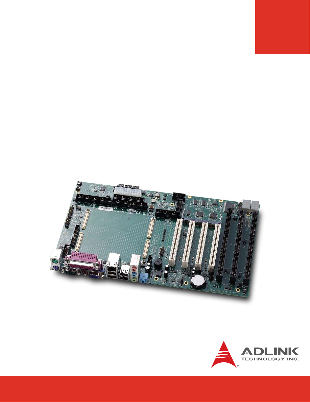
ETX-Proto
User’s Manual
Manual Revision: 2.00
Revision Date: May 18, 2010
Part Number: 50-1J028-1000
Page 2

Revision History
Release Date Change
1.00 2005/02/01 Initial release
2.00 2010/05/18 Update to PCB version B3
ETX-Proto User’s ManualPage 2
Page 3

Table of Contents
Preface ............................................................................................................................5
1 Introduction...............................................................................................................7
2 Special Functions .....................................................................................................8
2. 1 Secondary Super I/O ...........................................................................................................8
2.2 Carrier Hardware Monitor .................................................................................................... 8
2.3 Integrated Debug Port .........................................................................................................8
2.4 Audio Power Amplifier ..........................................................................................................8
2. 5 General Purpose I/O............................................................................................................8
2. 6 I2C and SMBus Devices ......................................................................................................9
3 Component Location ..............................................................................................10
4 Mechanical Dimensions..........................................................................................11
5 Function Diagram ...................................................................................................12
6 Connectors and Pinouts.........................................................................................13
6.1 ETX Module Signals .......................................................................................................... 13
6.2 Pin-Out Compatibillity ........................................................................................................13
6. 3 X1 Connector: PCI-bus, USB and Audio ...........................................................................14
6. 4 X2 Connector: ISA Bus .......................................................................................................15
6. 5 X3 Connector: CRT, LCD, Video, COM1/2, LPT1, IrDA, Mouse, Keyboard .................... 1 6
6. 6 X4 Connector: IDE1, IDE2, Ethernet, Miscellaneous .......................................................17
6.7 PCI and ISA Slots ...............................................................................................................18
6. 8 USB and LAN .....................................................................................................................22
6.9 Audio ..................................................................................................................................22
6.10 Video ..................................................................................................................................23
6. 11 I2C and SMBus ..................................................................................................................24
6.12 Keyboard & Mouse ............................................................................................................ 24
6.13 Serial and IrDA ...................................................................................................................25
6.14 Parallel Ports ......................................................................................................................26
6.15 Storage Devices .................................................................................................................27
Page 3ETX-Proto User’s Manual
Page 4

6.16 Pin Headers .......................................................................................................................29
6.17 Power Connectors .............................................................................................................30
6.18 Jumper Settings.................................................................................................................31
Important Safety Instructions......................................................................................34
Getting Service .............................................................................................................36
ETX-Proto User’s ManualPage 4
Page 5

Preface
Copyright 2010 ADLINK Technology, Inc.
This document contains proprietary information protected by copyright. All rights are
reserved. No part of this manual may be reproduced by any mechanical, electronic, or other
means in any form without prior written permission of the manufacturer.
Disclaimer
The information in this document is subject to change without prior notice in order to improve
reliability, design, and function and does not represent a commitment on the part of the
manufacturer.
In no event will the manufacturer be liable for direct, indirect, special, incidental, or consequential damages arising out of the use or inability to use the product or documentation,
even if advised of the possibility of such damages.
Environmental Responsibility
ADLINK is committed to fulfill its social responsibility to global environmental preservation
through compliance with the European Union's Restriction of Hazardous Substances (RoHS)
directive and Waste Electrical and Electronic Equipment (WEEE) directive. Environmental
protection is a top priority for ADLINK. We have enforced measures to ensure that our
products, manufacturing processes, components, and raw materials have as little impact on
the environment as possible. When products are at their end of life, our customers are
encouraged to dispose of them in accordance with the product disposal and/or recovery
programs prescribed by their nation or company.
Trademarks
AMIBIOS®8 is a registered trademarks of American Megatrends, Inc. COM Express™,
Express®, and PICMG® are registered trademarks of the PCI Industrial Computer
Manufacturers Group.
Product names mentioned herein are used for identification purposes only and may be
trademarks and/or registered trademarks of their respective companies.
Page 5ETX-Proto User’s Manual
Page 6
Conventions
Take note of the following conventions used throughout this manual to make sure that users
perform certain tasks and instructions properly.
Additional information, aids, and tips that help users perform tasks.
Information to prevent minor physical injury, component damage, data
loss, and/or program corruption when trying to complete a task.
Information to prevent serious physical injury, component damage, data
loss, and/or program corruption when trying to complete a specific task.
ETX-Proto User’s ManualPage 6
Page 7

1 Introduction
The ETX approach of custom carrier combined with off the shelf system core is an excellent
solution when you need to customize but lack the time or quantity for a complete redesign. It fits
most system integration projects with production volumes from 500 to 10,000 pcs per year. The
ETX concept has a great many advantages over full custom designs. It reduces engineering
complexity, lowers the threshold for total project quantity and last but not least brings your
product to the market in no time. The average time to design a carrier board is less than half the
time of a full custom OEM board.
ETX-Proto is a standard ATX size carrier board.Together with the ETX module of your choice and
off the shelf add-on cards, you can quickly emulate the functionality of your desired end
product for software development and hardware verification.
To build a functional prototype of your target system you will need:
f ETX module
f ETX-Proto
f ISA, PCI or Mini PCI add-on cards
f Storage or Flash disk solution
ETX Proto supports up to 4 PCI add-on cards and 3 ISA cards.
In addtion to the functions on the ETX module, ETX-Proto adds the following:
f Secondary I/O for COM3/4 and LPT2
f Secondary hardware monitor
f PCI based debug display for POST code readout
f I2C based GPIO
f Audio amplifier
Page 7ETX-Proto User’s Manual
Page 8

2 Special Functions
2.1 Secondary Super I/O
ETX-Proto uses the SMSC FDC37C669, an ISA based Super I/O chip to provide COM3,
COM4, LPT2 and FDD2 in addtion to the primary Super I/O on the ETX module. Support for
this secondary I/O is included standard in the BIOS of all ETX modules that support the ISA
bus.
2.2 Carrier Hardware Monitor
A W83782D Winbond H/W monitoring IC provides addtional hardware monitor functions. The
W83782D can be used to monitor several critical hardware parameters of the system that cannot
be monitored by the hardware monitor on the ETX module such as power supply voltages on
the carrier board, fan speeds, and system temperatures.
2.3 Integrated Debug Port
ETX-Proto supports an integrated debug port on board. The port 80 function is implemented with
two CPLD chips on the PCI bus interface.
2.4 Audio Power Amplifier
The onboard stereo audio power amplifier contains two identical amplifiers capable of delivering
6 W per channel of continuous average power into a 4-W load at 10% THD+N or 5 W per channel
at 1% THD+N. The gain of each channel is fixed at 20 dB. The amplifier features a mute/standby
function for power-sensitive applications.
2.5 General Purpose I/O
The F75111R is a low power general purpose IO chip providing 20 GPIO.
Most GPIO pins can be programmed to be power LEDs. Level or pulse modes can be
programmed by registers. Two power-down modes (Manual or Smart) can be selected to
save power and control the total consumption to under 10uA.
The F75111R also includes two sets of watchdog timers. One watchdog timer’s timeout unit
is set to seconds with a range of 0 to 127 seconds. The other Watchdog timer is set to
seconds or minutes and the range is 0 to 256 seconds or minutes.
ETX-Proto User’s ManualPage 8
Page 9

2.6 I2C and SMBus Devices
The SMBus (I2C bus) controller is integrated in the ETX core module. There are several
slave devices that reside on the SMBus (I2C bus) of the ETX-Proto. The addresses are as
follows:
Address Device Function Chipset
00101010 H/W monitor Winbond W83782D
10011100 GPIO & Watch Dog Timer Fintek F75111R
Page 9ETX-Proto User’s Manual
Page 10
3 Component Location
LED4
SLA3
LED5
8. 8.
SLA2
CN29
SLA1
PCI-4
CN2
PCI-3
CN32
JP6
JP8
JP10
JP11
JPX2
CN6
PH1
CN3
CN25
CN23
CN26
CN16
CN35
CN17
CN27
PCI-2
PCI-1
CN11
X2 X1
CN10
CNX1
BZ1
JPX1
CN5
CNY1CNY2 CNY3
JP1
CN4
CN7
JPY1
CN15
SW1 SW2
CN19
CN8
X4
CN21
CN22
X3
JP5
CNY4
CN14
CN13
CN12
ETX-Proto User’s ManualPage 10
Page 11
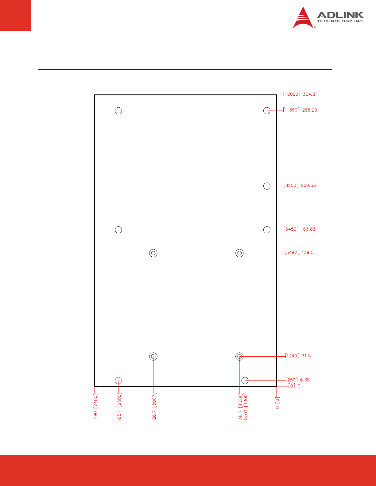
4 Mechanical Dimensions
Dimensions in mm [thou]
Page 11ETX-Proto User’s Manual
Page 12
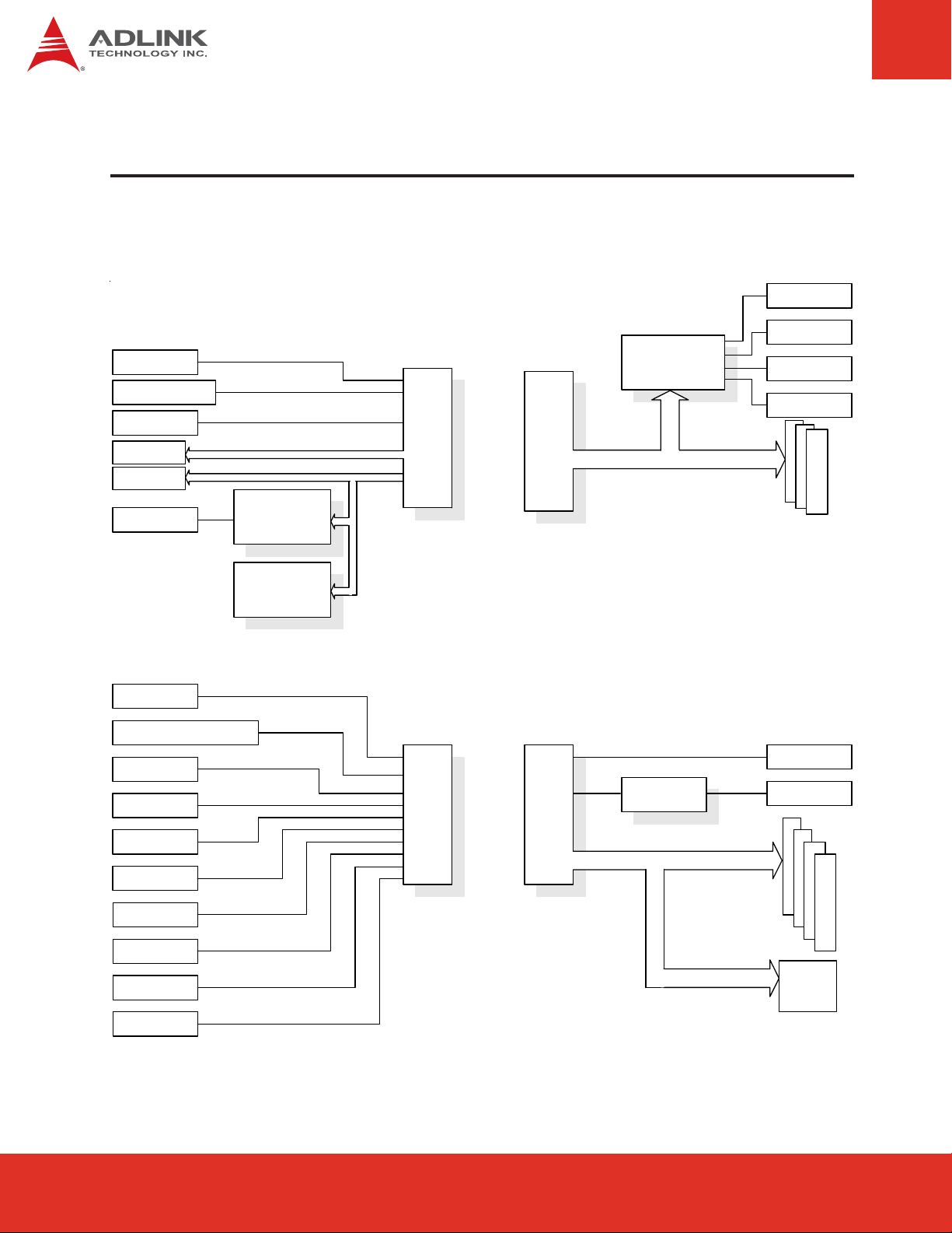
5 Function Diagram
2 ch. IDE
Power Signals
Ethernet
I2C bus
SMBus
20-bit GPIO
F75111R
20-bit GP I O
and Watchdog
W83782D
H/W Monitor
X4X3
FDC37C869
secondary
Super I/O
LPT2
COM3
COM4
FDD2
I
I
I
S
S
S
A
A
A
1
2
3
CRT VGA
Dual-Channel LVDS
Video-out
Keyboard
Mouse
LPT1
FDD
COM1
COM2
IrDA
X1 X2
Amplifier
4x USB
Audio
P
P
C
P
C
I
C
I
I
1
2
3
Mini
PCI
P
C
I
4
ETX-Proto User’s ManualPage 12
Page 13

6 Connectors and Pinouts
6.1 ETX Module Signals
- Ethernet
- IDE1 / IDE2
- Power Signals
- Speaker, Battery
2
- I
C & SMBus
- ISA bus
X4
X3
- VGA / LCD/ Video
- COM1 / COM 2
- LPT1
- IrDA
- Mouse
- Keyboard
X2
X1
- 32-bit PCI bus
- USB
- Audio
6.2 Pin-Out Compatibillity
All pin-outs on X1, X2, X3 and X4 on the ETX-Proto comply with pin-out and signal description used in the original “ETX Specification ver 2.6”. This document includes a description of
pin-outs, signal descriptions and mechanical characteristics of the ETX formfactor.
An addtional document called “ETX Design Guide” is a general introduction to carrier board
design for ETX core modules.
Page 13ETX-Proto User’s Manual
Page 14

6.3 X1 Connector: PCI-bus, USB and Audio
99 100
Signals and Pinout
Pin Signal Pin Signal
1 GND 2 GND
3 PCICLK3 4 PCICLK4
5 GND 6 GND
7 PCICLK1 8 PCICLK2
9 REQ3# 10 GNT3#
11 GNT2# 12 3V3
13 REQ2# 14 GNT1#
15 REQ1# 16 3V3
17 GNT0# 18 RESERVED
19 VCC 20 VCC
21 SERIRQ 22 REQ0#
23 AD0 24 3V3
25 AD1 26 AD2
27 AD4 28 AD3
29 AD6 30 AD5
31 C/BE0# 32 AD7
33 AD8 34 AD9
35 GND 36 GND
37 AD10 38 LINEIN_L
39 AD11 40 MICIN
41 AD12 42 LINEIN_R
43 AD13 44 AVCC
45 AD14 46 LINEOUT_L
47 AD15 48 AGND
49 C/BE1# 50 LINEOUT_R
21
Pin Signal Pin Signal
51 VCC 52 VCC
53 PAR 54 SERR#
55 PERR# 56 RESERVED
57 PME# 58 USB259 LOCK# 60 DEVSEL#
61 TRDY# 62 USB363 IRDY# 64 STOP#
65 FRAME# 66 USB2+
67 GND 68 GND
69 AD16 70 C/BE2#
71 AD17 72 USB3+
73 AD19 74 AD18
75 AD20 76 USB077 AD22 78 AD21
79 AD23 80 USB181 AD24 82 C/BE3#
83 VCC 84 VCC
85 AD25 86 AD26
87 AD28 88 USB0+
89 AD27 90 AD29
91 AD30 92 USB1+
93 PCIRST# 94 AD31
95 INTC# 96 INTD#
97 INTA# 98 INTB#
99 GND 100 GND
(1) Pins 12, 16, 24 are for 3.3 V power output, with combined capacity of 500 mA
ETX-Proto User’s ManualPage 14
Page 15

6.4 X2 Connector: ISA Bus
99 100
Signals and Pinout
Pin Signal Pin Signal
1 GND 2 GND
3 SD14 4 SD15
5 SD13 6 MASTER#
7 SD12 8 DREQ7
9 SD11 10 DACK7#
11 SD10 12 DREQ6
13 SD9 14 DACK6#
15 SD8 16 DREQ5
17 MEMW# 18 DACK5#
19 MEMR# 20 DREQ0
21 LA17 22 DACK0#
23 LA18 24 IRQ14
25 LA19 26 IRQ15
27 LA20 28 IRQ12(1)
29 LA21 30 IRQ11
31 LA22 32 IRQ10
33 LA23 34 IO16#
35 GND 36 GND
37 SBHE# 38 M16#
39 SA0 40 OSC
41 SA1 42 BALE
43 SA2 44 TC
45 SA3 46 DACK2#(2)
47 SA4 48 IRQ3
49 SA5 50 IRQ4
21
Pin Signal Pin Signal
51 VCC 52 VCC
53 SA6 54 IRQ5
55 SA7 56 IRQ6
57 SA8 58 IRQ7
59 SA9 60 SYSCLK
61 SA10 62 REFSH#
63 SA11 64 DREQ1
65 SA12 66 DACK1#
67 GND 68 GND
69 SA13 70 DREQ3
71 SA14 72 DACK3#
73 SA15 74 IOR#
75 SA16 76 IOW#
77 SA18 78 SA17
79 SA19 80 SMEMR#
81 IOCHRDY 82 AEN
83 VCC 84 VCC
85 SD0 86 SMEMW#
87 SD2 88 SD1
89 SD3 90 NOWS#
91 DREQ2(2) 92 SD4
93 SD5 94 IRQ9
95 SD6 96 SD7
97 IOCHK# 98 RSTDRV
99 GND 100 GND
(1) IRQ12 is reserved for PS/2 mouse; this pin is NC on the ETX-EV133.
(2) DREQ2/DACK2# is reserved for FDD controller; these pins are NC on ETX-EV133.
Page 15ETX-Proto User’s Manual
Page 16

6.5 X3 Connector: CRT, LCD, Video, COM1/2, LPT1,
IrDA, Mouse, Keyboard
99 100
Signals and Pinout
Pin Signal Pin Signal
1 GND 2 GND
3 RED 4 BLUE
5 HSYNC 6 GREEN
7 VSYNC 8 DDC2B_CLK
9 PAL_DETECT# 10 DDC2B_DAT
11 LCDDO16 12 LCDDO18
13 LCDDO17 14 LCDDO19
15 GND 16 GND
17 LCDDO13 18 LCDDO15
19 LCDDO12 20 LCDDO14
21 GND 22 GND
23 LCDDO8 24 LCDDO11
25 LCDDO9 26 LCDDO10
27 GND 28 GND
29 LCDDO4 30 LCDDO7
31 LCDDO5 32 LCDDO6
33 GND 34 GND
35 LCDDO1 36 LCDDO3
37 LCDDO0 38 LCDDO2
39 VCC 40 VCC
41 JILI_DAT 42 FLM
43 JILI_CLK 44 BLON#
45 BIASON 46 PLPWR_EN
47 TV_COMP 48 TV_Y
49 TV_SYNC 50 TV_C
21
Pin Signal Pin Signal
51 LPT/FLPY# 52 RESERVED
53 VCC 54 GND
55 STB# 56 AFD#
57 RESERVED 58 PD7
59 IRRX 60 ERR#
61 IRTX 62 P D 6
63 RXD2 64 INIT#
65 GND 66 GND
67 RTS2# 68 PD5
69 DTR2# 70 SLIN#
71 DCD2# 72 PD4
73 DSR2# 74 PD3
75 CTS2# 76 PD2
77 TXD2 78 PD1
79 RI2# 80 PD0
81 VCC 82 VCC
83 RXD1 84 ACK#
85 RTS1# 86 BUSY#
87 DTR1# 88 PE
89 DCD1# 90 SLCT#
91 DSR1# 92 MSCLK
93 CTS1# 94 MSDAT
95 TXD1 96 KBCLK
97 RI1# 98 KBDAT
99 GND 100 GND
(1) These pins are not connected.
ETX-Proto User’s ManualPage 16
Page 17

6.6 X4 Connector: IDE1, IDE2, Ethernet, Miscellaneous
99 100
Signals and Pinout
Pin Signal Pin Signal
1 GND 2 GND
3 5V_SB 4 PWGIN
5 PS_ON 6 SPEAKER
7 PWRBTN# 8 BATT
9 KBINH 10 LILED
11 RSMRST# 12 ACTLED
13 ROMKBCS#(1) 14 SPDLED
15 EXT_PRG(1) 16 I2CLK
17 VCC 18 VCC
19 OVCR# 20 GPCS#(1)
21 EXTSMI# 22 I2DAT
23 SMBCLK 24 SMBDATA
25 SIDE_CS3# 26 SMBALRT#
27 SIDE_CS1# 28 DASP_S(1)
29 SIDE_A2 30 PIDE_CS3#
31 SIDE_A0 32 PIDE_CS1#
33 GND 34 GND
35 PDIAG_S 36 PIDE_A2
37 SIDE_A1 38 PIDE_A0
39 SIDE_INTRQ 40 PIDE_A1
41 BATLOW# 42 GPE1#(2)
43 SIDE_ACK# 44 PIDE_INTRQ
45 SIORDY 46 PIDE_ACK#
47 SIDE_IOR# 48 PIORDY
49 VCC 50 VCC
21
Pin Signal Pin Signal
51 SIDE_IOW# 52 PIDE_IOR#
53 SIDE_DRQ 54 PIDE_IOW#
55 SIDE_D15 56 PIDE_DRQ
57 SIDE_D0 58 PIDE_D15
59 SIDE_D14 60 PIDE_D0
61 SIDE_D1 62 PIDE_D14
63 SIDE_D13 64 PIDE_D1
65 GND 66 GND
67 SIDE_D2 68 PIDE_D13
69 SIDE_D12 70 PIDE_D2
71 SIDE_D3 72 PIDE_D12
73 SIDE_D11 74 PIDE_D3
75 SIDE_D4 76 PIDE_D11
77 SIDE_D10 78 PIDE_D4
79 SIDE_D5 80 PIDE_D10
81 VCC 82 VCC
83 SIDE_D9 84 PIDE_D5
85 SIDE_D6 86 PIDE_D9
87 SIDE_D8 88 PIDE_D6
89 GPE2#(3) 90 CBLID_P#
91 RXD- 92 PIDE_D8
93 RXD+ 94 SIDE_D7
95 TXD- 96 PIDE_D7
97 TXD+ 98 HDRST#
99 GND 100 GND
(1) These pins are not connected.
(2) GPE1# is for case open detection.
(3) GPE2# is for system wake-up.
Page 17ETX-Proto User’s Manual
Page 18

6. 7 PCI and ISA Slots
PCI Interrupt Table
OnboardDevice Pin INTA# Pin INTB# Pin INTC# Pin INTD# IDSEL
PCI Slot 1 X1_INTAJ X1_INTDJ X1_INTCJ X1_INTBJ AD19
PCI Slot 2 X1_INTBJ X1_INTAJ X1_INTDJ X1_INTCJ AD20
PCI Slot 3 X1_INTCJ X1_INTBJ X1_INTAJ X1_INTDJ AD21
PCI Slot 4 X1_INTDJ X1_INTCJ X1_INTBJ X1_INTAJ AD22
Mini-PCI Slot X1_INTAJ X1_INTDJ AD22
ETX-Proto User’s ManualPage 18
Page 19

CN2: 32-bit Mini PCI Connector
Pin Signal Pin Signal
1NC 2NC
3NC 4NC
5NC 6NC
7NC 8NC
9NC 10NC
11 NC 12 NC
13 NC 14 NC
15 GND 16 NC
17 INTA# 18 +5V
19 +3.3V 20 INTD#
21 NC 22 NC
23 GND 24 +3.3V_SB
25 PCICLK 26 RST#
27 GND 28 +3.3V
29 REQ# 30 GNT#
31 +3.3V 32 GND
33 AD31 34 PME#
35 AD29 36 NC
37 GND 38 AD30
39 AD27 40 +3.3V
41 AD25 42 AD28
43 NC 44 AD26
45 CBE3# 46 AD24
47 AD23 48 IDSEL
49 GND 50 GND
51 AD21 52 AD22
53 AD19 54 AD20
55 GND 56 PAR
57 AD17 58 AD18
59 CBE2# 60 AD16
61 IRDY# 62 GND
Pin Signal Pin Signal
63 +3.3V 64 FRAME#
65 NC 66 TRDY#
67 SERR# 68 STOP#
69 GND 70 +3.3V
71 PERR# 72 DEVSEL#
73 CBE1# 74 GND
75 AD14 76 AD15
77 GND 78 AD13
79 AD12 80 AD11
81 AD10 82 GND
83 GND 84 AD 9
85 AD8 86 CBE0#
87 AD7 88 +3.3V
89 +3.3V 90 AD6
91 AD5 92 AD4
93 NC 94 AD2
95 AD3 96 AD0
97 +5V 98 NC
99 AD1 100 NC
101 GND 102 GND
103 NC 104 GND
105 NC 106 NC
107 NC 108 NC
109 NC 110 NC
111 NC 112 NC
113 NC 114 GND
115 NC 116 NC
117 NC 118 NC
119 NC 120 NC
121 NC 122 MPCIACT#
123 +5V_A 124 +3.3V_SB
Page 19ETX-Proto User’s Manual
Page 20

PCI1: 32-bit PCI slot (INTA#)
PCI2: 32-bit PCI slot (INTB#)
PCI3: 32-bit PCI slot (INTC#)
PCI4: 32-bit PCI slot (INTD# shared with CN2)
A Signal B Signal
1 TRST_L 1 -12V
2 +12V 2 TCK
3 TMS 3 Ground
4 TDI 4 TDO
5 +5V 5 +5V
6 INTA_L 6 +5V
7 INTC_L 7 INTB_L
8 +5V 8 INTD_L
9 Reserved 9 PRSNT1_L
10 +5V 10 Reserved
11 Reserved 11 PRSNT2_L
12 Ground 12 Ground
13 Ground 13 Ground
14 Reserved 14 Reserved
15 RST_L 15 Ground
16 +5V 16 CLK
17 GNT_L 17 Ground
18 Ground 18 REQ_L
19 Reserved 19 +5V
20 AD[30] 20 AD[31]
21 +3.3V 21 AD[29]
22 AD[28] 22 Ground
23 AD[26] 23 AD[27]
24 Ground 24 AD[25]
25 AD[24] +3.3V 25 +3.3V
26 IDSEL 26 C/BE[3]_L
27 +3.3V 27 AD[23]
28 AD[22] 28 Ground
29 AD[20] 29 AD[21]
30 Ground 30 AD[19]
31 AD[18] 31 +3.3V
A1
B1
A62
B62
A Signal B Signal
32 AD[16] 32 AD[17]
33 +3.3V 33 C/BE[2]_L
34 FRAME_L 34 Ground
35 Ground 35 IRDY_L
36 TRDY_L 36 +3.3V
37 Ground 37 DEVSEL_L
38 STOP_L 38 Ground
39 +3.3V 39 LOCK_L
40 Reserved 40 PERR_L
41 Reserved 41 +3.3V
42 Ground 42 SERR_L
43 PAR 43 +3.3V
44 AD[15] 44 C/BE[1]_L
45 +3.3V 45 AD[14]
46 AD[13] 46 Ground
47 AD[11] 47 AD[12]
48 Ground 48 AD[10]
49 AD[09] 49 Ground
50 KEYWAY 50 KEYWAY
51 KEYWAY 51 KEYWAY
52 C/BE[0]_L 52 AD[08]
53 +3.3V 53 AD[07]
54 AD[06] 54 +3.3V
55 AD[04] 55 AD[05]
56 Ground 56 AD[03]
57 AD[02] 57 Ground
58 AD[00] 58 AD[01]
59 +5V 59 +5V
60 REQ64_L 60 ACK64_L
61 +5V 61 +5V
62 +5V 62 +5V
ETX-Proto User’s ManualPage 20
Page 21

SLA1: 8/16-bit ISA slot
SLA2: 8/16-bit ISA slot
SLA3: 8/16-bit ISA slot
A1
B1 A31
A Signal B Signal
1 IOCHK# 1 GND
2 SD7 2 RSTDRV
3 SD6 3 +5V
4 SD5 4 IRQ9
5 SD4 5 +5V
6 SD3 6 DRQ2
7 SD2 7 -12V
8 SD1 8 NOWS#
9 SD0 9 +12V
10 IOCHRDY 10 GND
11 AEN 11 SMEMW#
12 SA19 12 SMEMR#
13 SA18 13 IOW#
14 SA17 14 IOR#
15 SA16 15 DACK#3
16 SA15 16 DRQ3
17 SA14 17 DACK#1
18 SA13 18 DRQ1
19 SA12 19 REFSH#
20 SA11 20 SYSCLK
21 SA10 21 IRQ7
22 SA9 22 IRQ6
23 SA8 23 IRQ5
24 SA7 24 IRQ4
25 SA6 25 IRQ3
26 SA5 26 DACK#2
27 SA4 27 TC
28 SA3 28 BALE
29 SA2 29 +5V
30 SA1 30 OSC
31 SA0 31 GND
B31D1C1 C18
D18
C Signal D Signal
1 SBHE# 1 MCS16#
2 LA23 2 IOCS#
3 LA22 3 IRQ10
4 LA21 4 IRQ11
5 LA20 5 IRQ12
6 SA19 6 IRQ14
7 SA18 7 IRQ15
8 SA17 8 DACK#0
9 MEMR# 9 DRQ0
10 MEMW# 10 DACK#5
11 SD8 11 DRQ5
12 SD9 12 DACK#6
13 SD10 13 DRQ6
14 SD11 14 DACK#7
15 SD12 15 DRQ7
16 SD13 16 +5V
17 SD14 17 MASTER#
18 SD15 18 GND
Page 21ETX-Proto User’s Manual
Page 22

6.8 USB and LAN
CN3: USB Connector
CN4: RJ-45 LAN
+ USB
Pin Signal
1 VCC
2 USB3 USB+
4 Ground
Pin Signal Function
1 TXDP Transmit Data(+)
2 TXDN Transmit Data(-)
3 RXDP Receive Data(+)
4 LANCT1 Termination
5 LANCT2 Termination
6 RXDN Receive Data(-)
7 LANCT3 Termination
8 LANCT4 Termination
Pin Signal
1 VCC
2 USB3 USB+
4 Ground
6.9 Audio
PH1: Audio
CN5: Audio CD-in
CN6: Audio Amplifier
Color Signal
PINK MIC IN
BLUE LINE IN
GREEN LINE OUT
1
2
3
4
Color Signal
1 LINR
2 AGND
3 AGND
4 LINL
Color Signal
BLACK Audio Out
ETX-Proto User’s ManualPage 22
Page 23

6.10 Video
CN7: VGA CRT
CN8: TV-out
CNY4: LVDS
Pin Signal Pin Signal
1 Red 2 Green
3 Blue 4 VCC pull-up
5 GND 6 GND
7 GND 8 GND
9 VCC 10 GND
11 VCC pull-up 12 DDC2B Data
13 HSYNC 14 Vsync
15 DDC2B clock
1
3
5
7
2
4
6
8
Pin Signal Pin Signal
1Y 2GND
3C 4GND
5 COMP 6 GND
7 SYNC 8 GND
Pin Signal Pin Signal
1 LVDS_I2C_DAT 2 LVDS_I2C_CK
3 N.C 4 N.C
5 GND 6 LVDS_A07 LVDS_A0+ 8 LVDS_VDD_EN
9 LVDS_A1- 10 LVDS_A1+
11 LVDS_BKLT_EN 12 LVDS_A2+
13 LVDS_A2- 14 N.C
15 LVDS_A_CK- 16 LVDS_A_CK+
17 N.C 18 LVDS_A3+
19 LVDS_A3- 20 GND
21 LVDS_B0- 22 LVDS_B0+
23 GND 24 LVDS_B125 LVDS_B1+ 26 GND
27 LVDS_B2- 28 LVDS_B2+
29 GND 30 LVDS_B_CK+
31 LVDS_B_CK- 32 N.C
33 LVDS_B3+ 34 LVDS_B3-
Page 23ETX-Proto User’s Manual
Page 24

6.11 I2C and SMBus
CN10: I2C bus
CN11: SMBus
6.12 Keyboard & Mouse
CN12: Mouse
(top)
1
2
3
4
1
2
3
4
65
4
21
3
Pin Signal
1 +5V
2 I2C_DATA
3 I2C_CLK
4 GND
Pin Signal
1 +5V
2 SMB_DATA
3 SMB_CLK
4 GND
Pin Signal
1 MSDAT
2NC
3 GND
4 KB5V
5 MSCLK
6NC
Keyboard
(bottom)
65
4
21
3
Pin Signal
1 KBDAT
2NC
3 GND
4 KB5V
5 KBCLK
6NC
ETX-Proto User’s ManualPage 24
Page 25

6.13 Serial and IrDA
CN13: COM1
CN14: COM2
CN25: COM3
CN26: COM4
Pin Signal Pin Signal
6 DSR 1 DCD
7RTS 2RXD
8 CTS 3 TXD
9 RI 4 DTR
5 GND
1
5
6
10
Pin Signal Pin Signal
1 DCD 6 DSR
2 RXD 7 RTS
3 TXD 8 CTS
4 DTR 9 RI
5 GND 10 NC
Page 25ETX-Proto User’s Manual
Page 26

6.14 Parallel Ports
CN15: LPT1
CN27: LPT2
1 14
13 26
Pin Signal Pin Signal
1 STROBE- 14 AUTO FEED2 DATA0 15 ERROR3 DATA1 16 INITIALIZE4 DATA2 17 SELECT INPUT5 DATA3 18 GND
6 DATA4 19 GND
7 DATA5 20 GND
8 DATA6 21 GND
9 DATA7 22 GND
10 ACKNOWLEDGE- 23 GND
11 BUSY 24 GND
12 PAPER EMPTY 25 GND
13 SELECT+ 26 N/C
Pin Signal Pin Signal
1 STROBE- 14 AUTO FEED2 DATA0 15 ERROR3 DATA1 16 INITIALIZE4 DATA2 17 SELECT INPUT5 DATA3 18 GND
6 DATA4 19 GND
7 DATA5 20 GND
8 DATA6 21 GND
9 DATA7 22 GND
10 ACKNOWLEDGE- 23 GND
11 BUSY 24 GND
12 PAPER EMPTY 25 GND
13 SELECT+ 26 N/C
ETX-Proto User’s ManualPage 26
Page 27

6.15 Storage Devices
CN16: FDD / LPT FDD Mode
To configure to FDD or LPT Mode,
see JP5 settings on p. 31.
1 2
33 34
Pin Signal Pin Signal
1 Ground 2 Driver density selection
3 Ground 4 N.C.
5 Ground 6 N.C.
7 Ground 8 Index
9 Ground 10 N.C.
11 Ground 12 Driver select 1
13 Ground 14 N.C.
15 Ground 16 Motor enable 1
17 Ground 18 Direction
19 Ground 20 Step
21 Ground 22 Write data
23 Ground 24 Write gate
25 Ground 26 Track 00
27 Ground 28 Write protect
29 Ground 30 Read data
31 Ground 32 Side 1 select
33 Ground 34 Diskette change
LPT Mode
Pin Signal Pin Signal
1 Ground 2 AUTO FEED3 Ground 4 N.C.
5 Ground 6 N.C.
7 Ground 8 DAT A 0
9 Ground 10 N.C.
11 Ground 12 ACKNOWLEDGE13 Ground 14 N.C.
15 Ground 16 BUSY
17 Ground 18 INITIALIZE19 Ground 20 SELECT INPUT 21 Ground 22 PAPER EMPTY
23 Ground 24 SELECT +
25 Ground 26 DAT A 1
27 Ground 28 DAT A 2
29 Ground 30 DAT A 3
31 Ground 32 ERROR 33 Ground 34 DAT A 4
Page 27ETX-Proto User’s Manual
Page 28

CN17: IDE0
CN19: IDE1
1 2
39 40
Pin Signal Pin Signal
1 Reset IDE 2 GND
3 IDE Data 7 4 IDE Data 8
5 IDE Data 6 6 IDE Data 9
7 IDE Data 5 8 IDE Data 10
9 IDE Data 4 10 IDE Data 11
11 IDE Data 3 12 IDE Data 12
13 IDE Data 2 14 IDE Data 13
15 IDE Data 1 16 IDE Data 14
17 IDE Data 0 18 IDE Data 15
19 Ground 20 KEY
21 DREQ0 22 GND
23 IDEIOW# 24 GND
25 IDEIOR# 26 GND
27 IDEIORDY 28 CBSEL
29 DACK0# 30 GND
31 IDEIRQ14 32 NC
33 IDE Address 1 34 PDIAG#
35 IDE Address 0 36 IDE Address 2
37 IDE Chip select 1# 38 IDE Chip select 3#
39 IDE activity 40 GND
ETX-Proto User’s ManualPage 28
Page 29

6.16 Pin Headers
CN21: Miscellaneous Connector
1 11
10 20
CN22: X4 Extension Header
1 2
11 12
Pin Signal Pin Signal
1 Power LED 11 Speaker
2 Power LED 12 Speaker
3 Power LED 13 Speaker
4 Keyboard Lock 14 Speaker
5 Keyboard Lock 15 RESET
6 NC 16 RESET
7 NC 17 HDD LED
8 NC 18 HDD LED
9 NC 19 Power Button
10 NC 20 Power Button
Pin Signal Pin Signal
1 +5V 7 X4_RSMRSTJ
2 X4_GPE1J 8 X4_EXTSMI
3 X4_SMBLARTJ 9 X1_SERIRQ
4 X4_GPE2J 10 X4_GPCSJ
5 BATLOWJ 11 GND
6 ROMKBCSJ 12 X4_EXTPRG
CN29: GPIO Header
20 11
2 1
Pin Signal Pin Signal
1 GPIO01 2 GPIO11
3 GPIO02 4 GPIO12
5 GPIO03 6 GPIO13
7 GPIO04 8 GPIO14
9 GPIO05 10 GPIO15
11 GPIO06 12 GPIO16
13 GPIO07 14 GPIO17
15 GPIO08 16 GPIO18
17 GPIO09 18 GPIO19
19 GPIO10 20 GPIO20
Page 29ETX-Proto User’s Manual
Page 30

6.17 Power Connectors
CN23: ATX Power Connector
AT Power Connectors
1
+3.3 V
Power On
CNY1
DC
-12 V
DC
Ground
Ground
Ground
Ground
-5 V
DC
+5 V
DC
+5 V
DC
11
12
13
14
15
16
17
18
19
20
Pin Signal
1 GND
23 P12V
1
2
3
4
5
6
7
8
9
10
+3.3 V
+3.3 V
DC
DC
Ground
+5 V
DC
Ground
+5 V
DC
Ground
Power Good
+5 V
+12 V
Standby
DC
DC
CNY2
CNY3
Pin Signal
1 5VCC
2 5VCC
3 5VCC
Pin Signal
1 GND
2 GND
3 GND
ETX-Proto User’s ManualPage 30
Page 31

6.18 Jumper Settings
JP1: LAN Termination
JP5: Printer/Floppy Mode
JP6: Reserved
JP8: Clear CMOS
1
2
3
1
2
3
1
2
3
Combination Signal
1-2 Power decouple
2-3 GND decouple
Combination Signal
1-2 Printer enabled
2-3 Floppy enabled
Combination Signal
1-2 Normal
2-3 Clear
JPX1: Enable Buzzer
JPX2: Enable Backlight
1
2
3
1
2
3
Combination Signal
1-2 Enable
2-3 Normal
Combination Signal
1-2 Convert
2-3 Normal
Page 31ETX-Proto User’s Manual
Page 32

I2C/SMBus Buffers
These buffers settings are for isolation of the I2C and SMBus - test feature only.
On: I2C/SMBus passes through LTC4300A-2 Buffer
Off: Bypass Buffer
JPX3: I2C Buffer (Data)
1
2
3
Combination Signal
1-2 On
2-3 Off
JPX4: I2C Buffer (Clock)
1
2
3
Combination Signal
1-2 On
2-3 Off
JPX5: SMBus Buffer (Data)
1
2
3
Combination Signal
1-2 On
2-3 Off
JPX6: SMBus Buffer (Clock)
JPY1: Power Supply Mode
1
2
3
1
2
3
Combination Signal
1-2 On
2-3 Off
Combination Signal
1-2 ATX Mode
2-3 AT Mode
ETX-Proto User’s ManualPage 32
Page 33

This page intentionally left blank.
Page 33ETX-Proto User’s Manual
Page 34

Important Safety Instructions
For user safety, please read and follow all instructions, warnings, cautions, and notes
marked in this manual and on the associated equipment before handling/operating the
equipment.
f Read these safety instructions carefully.
f Keep this user’s manual for future reference.
f Read the specifications section of this manual for detailed information on the operating
environment of this equipment.
f When installing/mounting or uninstalling/removing equipment:
- Turn off power and unplug any power cords/cables.
f To avoid electrical shock and/or damage to equipment:
- Keep equipment away from water or liquid sources;
- Keep equipment away from high heat or high humidity;
- Keep equipment properly ventilated (do not block or cover ventilation openings);
- Make sure to use recommended voltage and power source settings;
- Always install and operate equipment near an easily accessible electrical socketoutlet;
- Secure the power cord (do not place any object on/over the power cord);
- Only install/attach and operate equipment on stable surfaces and/or recommended
mountings; and,
- If the equipment will not be used for long periods of time, turn off and unplug the
equipment from its power source.
f Never attempt to fix the equipment. Equipment should only be serviced by qualified
personnel.
f A Lithium-type battery may be provided for uninterrupted, backup or emergency power.
Risk of explosion if battery is replaced by an incorrect type. Dispose of used batteries
according to the instructions.
ETX-Proto User’s ManualPage 34
Page 35

f Equipment must be serviced by authorized technicians when:
- The power cord or plug is damaged;
- Liquid has penetrated the equipment;
- It has been exposed to high humidity/moisture;
- It is not functioning or does not function according to the user’s manual;
- It has been dropped and/or damaged; and/or,
- It has an obvious sign of breakage.
Page 35ETX-Proto User’s Manual
Page 36

Getting Service
Contact us should you require any service or assistance.
ADLINK Technology, Inc.
Address: 9F, No.166 Jian Yi Road, Chungho City,
Taipei County 235, Taiwan
קᗼխࡉؑ৬ԫሁ 166 ᇆ 9 ᑔ
Tel: +886-2-8226-5877
Fax: +886-2-8226-5717
Email: service@adlinktech.com
Ampro ADLINK Technology, Inc.
Address: 5215 Hellyer Avenue, #110, San Jose, CA 95138, USA
Tel: +1-408-360-0200
Toll Free: +1-800-966-5200 (USA only)
Fax: +1-408-360-0222
Email: info@adlinktech.com
ADLINK Technology Beijing
Address: ࣫ҀᏖ⍋⎔Ϟഄϰ䏃 1 োⲜ߯ࡼ E ᑻ 801 ᅸ(100085)
Rm. 801, Power Creative E, No. 1, B/D
Shang Di East Rd., Beijing, 100085 China
Tel: +86-10-5885-8666
Fax: +86-10-5885-8625
Email: market@adlinktech.com
ADLINK Technology Shanghai
Address: Ϟ⍋Ꮦⓩ⊇⋒催⾥ᡔᓔথ䩺∳䏃 333 ো 39 ᐶ 4 ሖ (200233)
4F, Bldg 39, Caoheting Science & Technology Park,
No.333 Qinjiang Rd., Shanghai, 200233 China
Tel: +86-21-6495-5210
Fax: +86-21-5450-0414
Email: market@adlinktech.com
ADLINK Technology Shenzhen
Address: ⏅ഇᏖቅ⾥ᡔು催ᮄϗ䘧᭄ᄫᡔᴃು
A1 2 ὐ C (518057)
2F, C Block, Bldg. A1, Cyber-Tech Zone, Gao Xin Ave. Sec. 7,
High-Tech Industrial Park S., Shenzhen, 518054 China
Tel: +86-755-2643-4858
Fax: +86-755-2664-6353
Email: market@adlinktech.com
ETX-Proto User’s ManualPage 36
Page 37

ADLINK Technology, Inc. (German Liaison Office)
Address: Nord Carree 3, 40477 Duesseldorf, Germany
Tel: +49-211-495-5552
Fax: +49-211-495-5557
Email: emea@adlinktech.com
ADLINK Technology, Inc. (French Liaison Office)
Address: 15 rue Emile Baudot, 91300 Massy CEDEX, France
Tel: +33 (0) 1 60 12 35 66
Fax: +33 (0) 1 60 12 35 66
Email: france@adlinktech.com
ADLINK Technology Japan Corporation
Address: 151-0072 ᧲ㇺ⼱ᐈ䊱⼱㩷
1-1-2 ᦺᣣ↢ᐈ䊱⼱䊎䊦 8F
Asahiseimei Hatagaya Bldg. 8F
1-1-2 Hatagaya, Shibuya-ku, Tokyo 151-0072, Japan
Tel: +81-3-4455-3722
Fax: +81-3-5333-6040
Email: japan@adlinktech.com
ADLINK Technology, Inc. (Korean Liaison Office)
Address: 昢殾柢 昢爎割 昢爎壟 1506-25 穢壊 B/D 2 猻
2F, Hando B/D, 1506-25, Seocho-Dong, Seocho-Gu,
Seoul 137-070, Korea
Tel: +82-2-2057-0565
Fax: +82-2-2057-0563
Email: korea@adlinktech.com
ADLINK Technology Singapore Pte. Ltd.
Address: 84 Genting Lane #07-02A, Cityneon Design Centre,
Singapore 349584
Tel: +65-6844-2261
Fax: +65-6844-2263
Email: singapore@adlinktech.com
ADLINK Technology Singapore Pte. Ltd. (Indian Liaison Office)
Address: No. 1357, "Anupama", Sri Aurobindo Marg, 9th Cross,
JP Nagar Phase I, Bangalore - 560078, India
Tel: +91-80-65605817
Fax: +91-80-22443548
Email: india@adlinktech.com
Page 37ETX-Proto User’s Manual
Page 38

 Loading...