

Page 1
ETX
ETX-CV
User’s Manual
Manual Revision: 2.03
Revision Date: May 7, 2015
Part Number: 50-1J041-1030
Page 2

Revision History
Revision Date Change(s)
2.00 2013/09/02 Initial release
2.01 2013/10/25 Update LVDS resolution spec
2.02 2014/11/14 Remove FDD support
2.03 2015/05/07 Correct Ethernet chip
ETX-CV User’s ManualPage 2
Page 3

Table of Contents
Preface ............................................................................................................................5
1 Introduction...............................................................................................................7
1.1 Description............................................................................................................................7
2 Specifications ...........................................................................................................8
2.1 General .................................................................................................................................8
2.2 Integrated Video....................................................................................................................8
2.3 Audio.....................................................................................................................................9
2.4 LAN.......................................................................................................................................9
2.5 Multi I/O ................................................................................................................................9
2.6 Super I/O ..............................................................................................................................9
2.7 TPM (Trusted Platform Module)............................................................................................9
2.8 Power Specifications...........................................................................................................10
2.9 Operating Systems Support................................................................................................11
2.10 Mechanical and Environmental ........................................................................................... 11
2.11 Ordering Information ...........................................................................................................11
3 Function Diagram ...................................................................................................12
4 Mechanical Dimensions.........................................................................................13
5 Embedded Functions .............................................................................................14
5.1 Watchdog Timer..................................................................................................................14
5.2 Hardware Monitoring...........................................................................................................15
6 Pin-out and Signal Descriptions ...........................................................................16
6.1 Connector Locations...........................................................................................................16
6.2 Pin Compatibility .................................................................................................................16
6.3 Pin Definitions.....................................................................................................................17
6.4 Signal Descriptions .............................................................................................................22
7 System Resources..................................................................................................31
7.1 System Memory Map..........................................................................................................31
7.2 I/O Address Map .................................................................................................................32
7.3 Interrupt Request (IRQ) Lines.............................................................................................34
7.4 PCI Configuration Space Map.............................................................................................35
ETX-CV User’s Manual Page 3
ETX-CV User’s Manual Page 3
Page 4

7.5 PCI Interrupt Routing Map ..................................................................................................36
7.6 System Management Bus (I2C-compatible)........................................................................36
8 BIOS Setup Utility...................................................................................................37
8.1 Starting the BIOS................................................................................................................37
8.2 Main Setup..........................................................................................................................42
8.3 Advanced BIOS Setup ........................................................................................................43
8.4 Chipset Configuration .........................................................................................................61
8.5 Boot Setup ..........................................................................................................................65
8.6 Security Setup.....................................................................................................................68
8.7 Save & Exit .........................................................................................................................69
9 BIOS Checkpoints, Beep Codes............................................................................ 71
9.1 Status Code Ranges...........................................................................................................72
9.2 Standard Status Codes.......................................................................................................72
9.3 OEM-Reserved Status Code Ranges .................................................................................78
Appendix A: Connectors and Mounting.....................................................................79
A.1 Carrier Board ETX Connecter Heights (Hirose FX8/FX8C Receptacles)...........................79
A.3 Mounting Procedures..........................................................................................................80
A.4 Standoff T ypes - Carrier Board ...........................................................................................81
Important Safety Instructions .....................................................................................82
Getting Service.............................................................................................................84
ETX-CV User’s ManualPage 4
Page 5

Preface
Copyright 2013-15 ADLINK Technology, Inc.
This document contains proprietary information protected by copyright. All rights are reserved. No
part of this manual may be reproduced by any mechanical, electronic, or other means in any form
without prior written permission of the manufacturer.
Disclaimer
The information in this document is subject to change without prior notice in order to improve
reliability, design, and function and does not represent a commitment on the part of the
manufacturer.
In no event will the manufacturer be liable for direct, indirect, special, incidental, or consequential
damages arising out of the use or inability to use the product or documentation, even if advised
of the possibility of such damages.
Environmental Responsibility
ADLINK is committed to fulfill its social responsibility to global environmental preservation
through compliance with the European Union's Restriction of Hazardous Substances (RoHS)
directive and Waste Electrical and Electronic Equipment (WEEE) directive. Environmental
protection is a top priority for ADLINK. We have enforced measures to ensure that our products,
manufacturing processes, components, and raw materials have as little impact on the
environment as possible. When products are at their end of life, our customers are encouraged to
dispose of them in accordance with the product disposal and/or recovery programs prescribed by
their nation or company.
Trademarks
AMI Aptio® is a registered trademark of American Megatrends, Inc. ETX® is a registered
trademark of Kontron Embedded Modules GmbH.
Product names mentioned herein are used for identification purposes only and may be
trademarks and/or registered trademarks of their respective companies.
ETX-CV User’s Manual Page 5
ETX-CV User’s Manual Page 5
Page 6

Conventions
Take note of the following conventions used throughout this manual to make sure that users
perform certain tasks and instructions properly.
Additional information, aids, and tips that help users perform tasks.
Information to prevent minor physical injury, component damage, data loss,
and/or program corruption when trying to complete a task.
Information to prevent serious physical injury, component damage, data
loss, and/or program corruption when trying to complete a specific task.
ETX-CV User’s ManualPage 6
Page 7

1 Introduction
1.1 Description
The ETX-CV is an ETX v3.02 compliant module specially designed to facilitate speedy
development of semi custom designs. ETX is an open standard that targets the market for
embedded OEM projects. An ETX core combined with a custom made carrier board represents a
value solution that allows OEM customers to get to the market fast. The new ETX v3.02
specification adds SATA support to ETX in the form of two connectors on the module itself,
leaving the ETX board-to-board interface 100% compatible with baseboards designed under the
earlier ETX v2.xx specification.
The ETX-CV is positioned as an entry level ETX module for generic systems but also for systems
requiring a full set of graphics features. The module comes with integrated support for high VGA
up to 1920 x 1200 resolution (WUXGA), single/dual channel 18/24-bit LVDS and onboard
DisplayPort connector.
The ETX-CV conforms to the latest ETX® 3.02 specification and provides two additional onboard
SATA connectors while maintaining full backward compatibility with earlier ETX® standards.
Operating system support includes Windows XP, Windows XP Embedded, Windows 7, WinCE,
and Linux. Primary focus is for applications in Medical Diagnostics and Imaging, Gaming,
Industrial Automation, Test and Measurement, POS, and Industrial Control.
The dual-core Intel® Atom™ Processor N2000 and D2000 Series on the ETX-CV replaces the
previous generation Intel® Atom™ processors N4xx/N5xx. Although much smaller in size, Intel®
Atom™ processors share the same architecture as Intel® Core™2 Duo processors and
additionally support Intel® Hyper-Threading Technology, allowing more than one code thread to
be executed at the same time on a single core. The ETX-CV's thermal design and powerful CPU
core allow it to provide the same or even better performance than earlier generation modules at a
more modest power consumption.
The ETX-CV supports up to 4 GB of DDR3 memory on a single SODIMM, incorporates an Intel
10/100BASE-T Ethernet controller, and provides dual channel IDE, two channels SATA, four USB
2.0 ports, two serial ports, one parallel port, one PS/2 keyboard/mouse interface and HD audio.
The ETX-CV fully supports PCI and legacy ISA based on high speed PCI/ISA bridge and is
equipped with an AMI Aptio BIOS supporting embedded features such as Remote Console,
CMOS backup for battery-less operation, CPU and System Monitoring and Watchdog Timer.
The ETX-CV is a RoHS compliant and leadfree product.
ETX-CV User’s Manual Page 7
ETX-CV User’s Manual Page 7
Page 8

2 Specifications
2.1 General
f CPU: Intel® Atom™ N2600 1.66GHz with 1MB L2 cache, 3.5W
Intel® Atom™ N2800 1.83GHz with 1MB L2 cache, 6.5W
Intel® Atom™ D2550 1.86GHz with 1MB L2 cache, 10W
- On-die primary 32-kB instructions cache and 24-kB write back data cache
- Intel® Hyper-Threading Technology, 2-threads per core
- Supports C0 and C1 states only for D2550
- Supports C0-C4, C1E-C4E and Deep Power Down Technology (code named C6)
for N2600/N2800
f Memory: Single SODIMM socket supporting:
- up to 4 GB of non-ECC, un-buffered, 1066 MHz standard DDR3 SODIMM memory
f Chipset: Intel® NM10 Express chipset
f BIOS: AMI Aptio UEFI on 16Mbit SPI flash
f Hardware Monitor: Supply voltages and CPU temperature
f Watchdog Timer: Programmable timer ranges to generate RESET
f Expansion Busses: 32-bit PCI 2.3 Masters at 33 MHz
2.2 Integrated Video
f GPU: Integrated in CPU, supports dual independent displays
f VGA Interface: Analog RGB support by 350Hz RAMDAC, resolution up to 1920 x1200
(WUXGA) @ 60Hz
f LVDS Interface:
- single/dual channel 18/24-bit with resolution up to 1920 x1200
ISA 16-bit (via PCI/ISA bridge), no DMA support
SMBus/I2C
ETX-CV User’s ManualPage 8
Page 9

2.3 Audio
f Audio Codec: Realtek ALC262 HDA
2.4 LAN
f Chipset: Realtek RTL8111E
f Interface: 10/100 Mbps with Wake-on-LAN and Alert on LAN support
2.5 Multi I/O
f IDE (PATA): Two channels IDE with UDMA 100 support
f SATA: Two channels SATA 3Gb/s with connectors on module
f USB: Supports up to four ports USB 2.0
2.6 Super I/O
f Chipset: W83627DHG-PT
f Serial: Two high speed RS-232C ports (COM1/COM2)
f IrDA: SIR IrDA 1.1 compliant
f Parallel: SPP, EPP, and ECP mode
f Keyboard & Mouse: One PS/2 keyboard and one PS/2 mouse
2.7 TPM (Trusted Platform Module)
f Chipset: Infineon SLB9635TT1.2
f Type: TPM 1.2
ETX-CV User’s Manual Page 9
ETX-CV User’s Manual Page 9
Page 10

2.8 Power Specifications
f Input Power: AT mode and ATX mode
f Power Management: ACPI 3.0 compliant with battery support
f Power States: supports S0, S1, S3, S4, S5
Test Configuration
Function Configuration
Memory Transcend 4GB DDR3 1333 SODIMM (I) (SEC 107 HCH9K4B260846C)
Graphics Intel® Atom® N2000/D2000 Series Embedded Media and Graphics Driver
Hard Drive Seagate ST320LT020 MomentusThin 320G
Backplane ETX-Proto B3
Power Supply FSP FSP350-60PFG 350W
Intel® Atom™ Processor N2600 1.66Gz, (1MB L2 cache, 3.5W)
Power State Power Requirement Current Power
Windows 7 logon screen (idle) +5V (4.88V) 1.29A 6.30W
Max. Load (Intel Power Utility Tool) +5V (4.86V) 2.04A 9.91W
S5 Mode (soft off) 5V Standby 0.06A 0.30W
S3 Mode (suspend to RAM) 5V Standby 0.07A 0.35W
Intel® Atom™ Processor N2800 1.86Gz, (1MB L2 cache, 6.5W)
Power State Power Requirement Current Power
Windows 7 logon screen (idle) +5V (4.82V) 1.52A 7.33W
Max. Load (Intel Power Utility Tool) +5V (4.80V) 2.83A 13.58W
S5 Mode (soft off) 5V Standby 0.07A 0.35W
S3 Mode (suspend to RAM) 5V Standby 0.09A 0.45W
Intel® Atom™ Processor D2550 1.86GHz, (1MB L2 cache, 10 W)
Power State Power Requirement Current Power
Windows 7 logon screen (idle) +5V (4.88V) 1.78A 8.69W
Max. Load (Intel Power Utility Tool) +5V (4.84V) 2.89A 13.99W
S5 Mode (soft off) 5V Standby 0.057A 0.29W
S3 Mode (suspend to RAM) 5V Standby 0.09A 0.45W
ETX-CV User’s ManualPage 10
Page 11

2.9 Operating Systems Support
f Standard Support
- Windows 7 32-bit
- Windows Embedded Compact 7
- Linux 2.8
f Extended Support (BSP)
- Embedded XP BSP
- WinCE 6.0 BSP
- Linux 2.6.x BSP
f Libraries, API support
- AIDI I2C Library for Win32, WinCE and Linux
2.10 Mechanical and Environmental
f Form factor and Type: ETX rev 3.02
f Dimensions: 95 x 114 mm
f Standard Operating Temperature: 0°C to 60°C
f Relative Humidity: 5% to 95%
f Shock : 15G peak-to-peak, 11ms duration, non-operation
f Vibration:
Non-operating : 1.88 Grms, 5-500 Hz, each axis
Operating : 0.5 Grms, 5-500 Hz, each axis
f Certification : CE, FCC
2.11 Ordering Information
f ETX-CV-N2600
ETX Module with low power Dual Core Intel® Atom™ Processor N2600 (1.66GHz)
with NM10 Chipset
f ETX-CV-N2800
ETX Module with low power Dual Core Intel® Atom™ Processor N2800 (1.83GHz)
with NM10 Chipset
f ETX-CV-D2550
ETX Module with Dual Core Intel® Atom™ Processor D2550 (1.86GHz)
with NM10 Chipset
ETX-CV User’s Manual Page 11
ETX-CV User’s Manual Page 11
Page 12
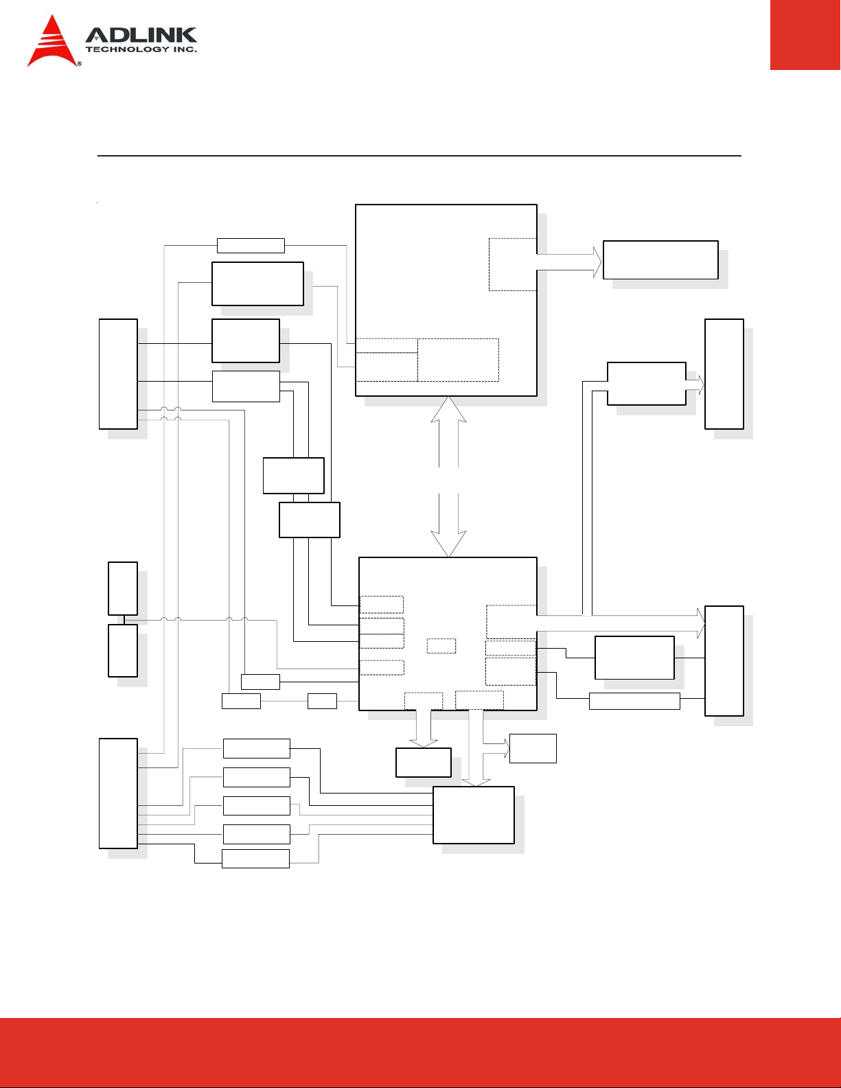
3 Function Diagram
X4X3
SATA
SATA
VGA
DP to LVDS
Chrontel
CH7511
LAN PHY
Realtek
RTL8111E
PATA
IDE0/IDE1
PCIe-to-PATA
SMBus
I2C
Marvell
88SE6101
PCIe-to-PATA
Marvell
88SE6101
BC
Analog VGA
DP/HDMI
Intel® NM10
PCIe x1
PCIe x1
PCIe x1
SATA
CPU
Intel® Atom™
N2600
N2800
D2550
Graphics Core
640 MHz
2.5 GT/s DMI
Chipset
RTC
SPI
LPC
DDR3
Memory
Controller
PCI
Controller
Audio
USB 2.0
PCI / ISA
PCI Bus
Audio Codec
4 ports USB 2.0
SODIMM
DDR3 1066 MHz
IT8888G
Realtek
ALC262
X2X1
Keyboard
Mouse
LPT1/FDD
COM1
COM2
BIOS
Debug
Header
Super I/O
Winbond
W83627DHG
ETX-CV User’s ManualPage 12
Page 13
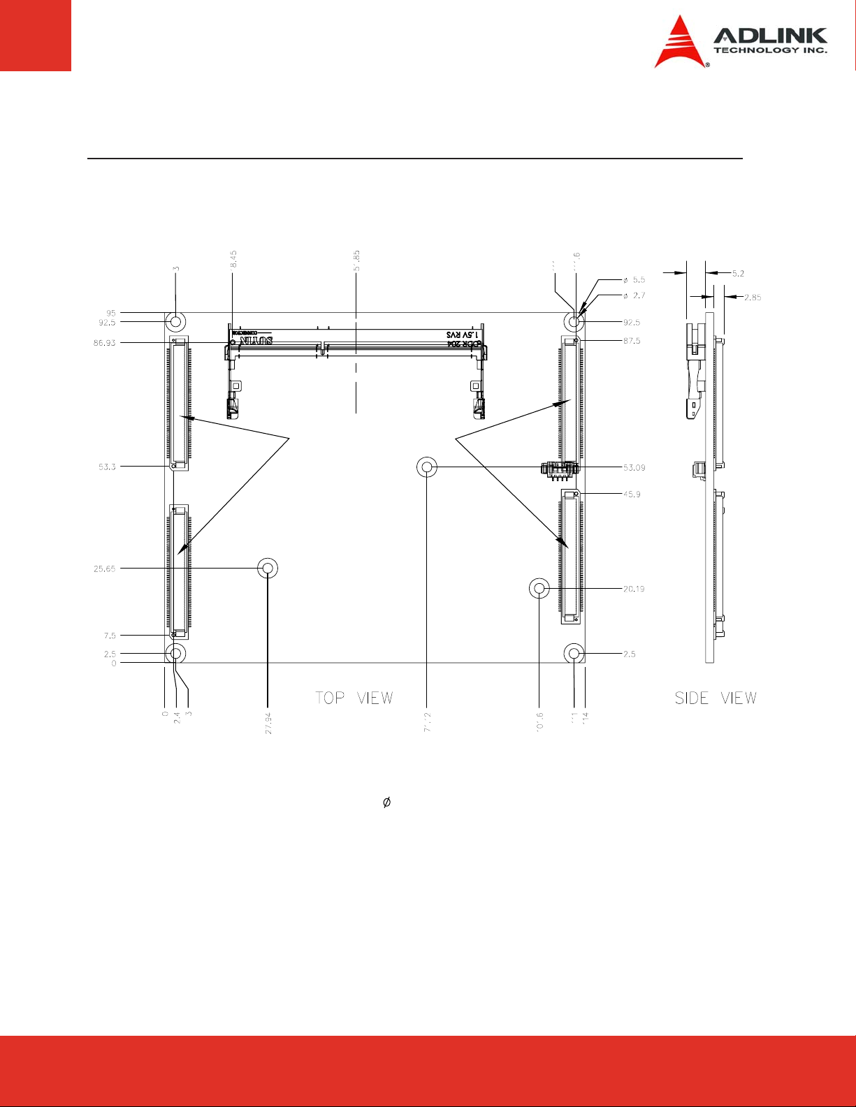
4 Mechanical Dimensions
Connector on bottom side
All tolerances ± 0.05 mm
Other tolerances ± 0.2 mm
ETX-CV User’s Manual Page 13
ETX-CV User’s Manual Page 13
Page 14
5 Embedded Functions
All embedded board functions on ADLINK’s Computer on Modules are supported at the operating
system level using the ADLINK Intelligent Device Interface (AIDI) library. The AIDI API
programming interface is compatible and identical across all supported ADLINK Computer on
Modules and all supported operating systems. The AIDI library includes a demo program to
demonstrate the library’s functionallity.
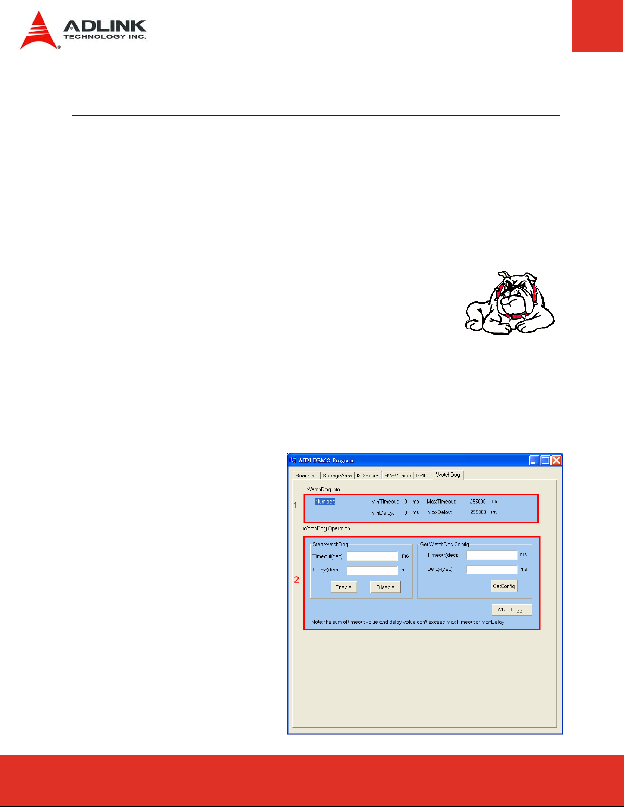
5.1 Watchdog Timer
The ETX-CV implements a Watchdog timer that can be used to
automatically detect software execution problems or system hangs and
reset the board if necessary. The Watchdog timer consists of a counter
that counts down from an initial value to zero. When the system is
operating normally, the software that sets the intial value periodically
resets the counter so that the it never reaches zero. If the counter
reaches zero before the software resets it, the system is presumed to be
malfunctioning and a reset signal is asserted.
The AIDI Library Watchdog functions support Watchdog control of the board. If the Watchdog
begins countdown and reaches zero, it will access the CPU's RESET signal to reset the system.
This application must call another function named AidiWDogTrigger that triggers the Watchdog to
restart to prevent system reset.
AIDI Demo Program
- Watchdog Tab
The AIDI Demo Program allows
retrieval of the current Watchdog
status and updating of the
Watchdog settings
If the Watchdog is enabled, the
user can click the WDT Trigger
button to manually reset the
counter and prevent the system
from resetting
ETX-CV User’s ManualPage 14
Page 15
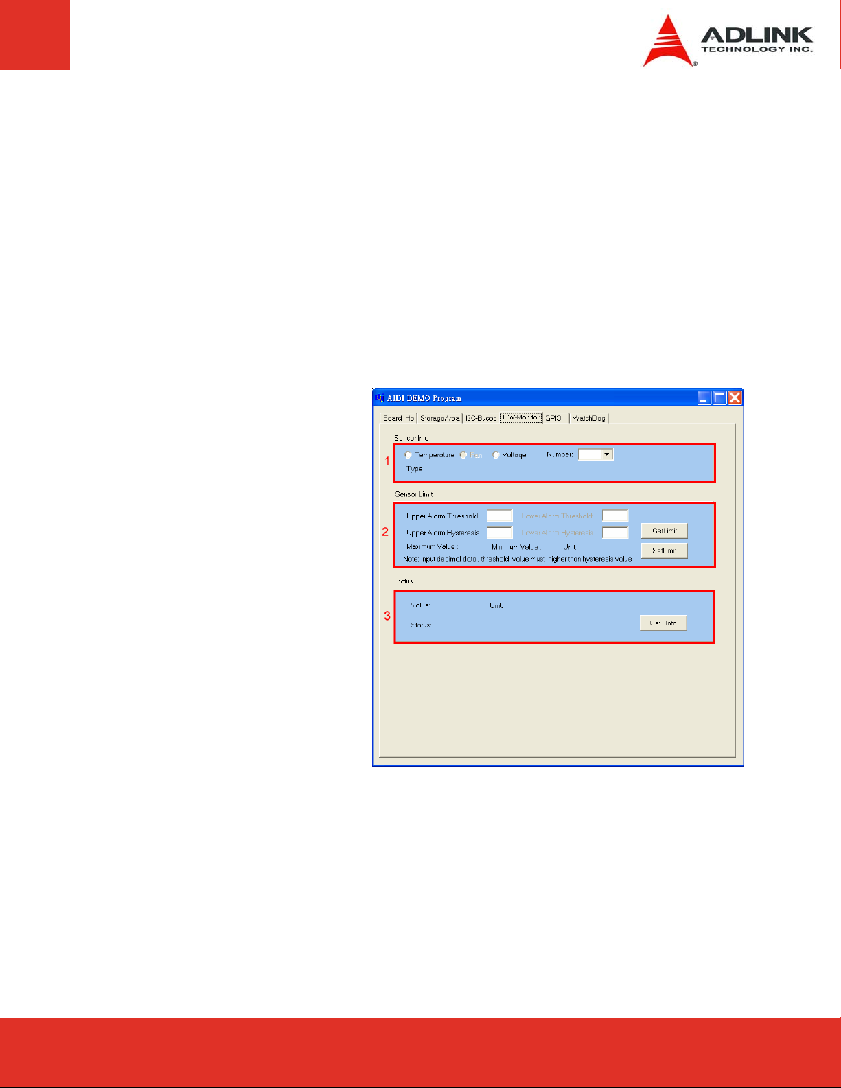
5.2 Hardware Monitoring
To ensure system health of your embedded system ADLINK’s Computer on Modules come with
built in support for monitoring of CPU temperatures and critical module voltage levels.
The AIDI Library provides simple APIs at the application level to support these functions and adds
alarm functions when voltage or temperature levels exceeds the upper or lower limit set by the
user.
On the ETX-CV the following monitored values can be read from the module:
CPU temperature, Vcore, 1.05V, 3.3V, 5V and VBAT.
AIDI Demo Program
- HW Monitor Tab
Field 1 displays detected sensors
(number).
Field 2 allows setting of upper and
lower alarm limits.
Field 3 displays read out
information of sensors.
ETX-CV User’s Manual Page 15
ETX-CV User’s Manual Page 15
Page 16
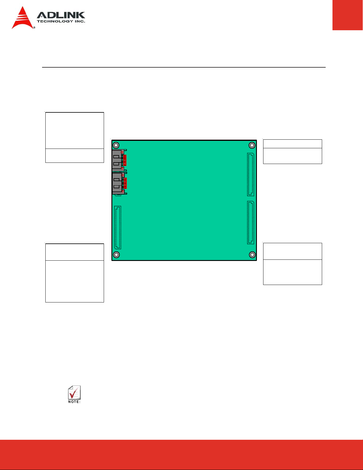
6 Pin-out and Signal Descriptions
6.1 Connector Locations
- Ethernet
- IDE1/IDE2
- Power Signals
- Speaker, Battery
2
- I
C & SMB bus
- ISA bus
X4
X3
- VGA/LCD/Video
- COM1/COM2
- LPT1
- IrDA
- Mouse
- Keyboard
X2
ETX-CV
(top view)
X1
- 32-bit PCI bus
- USB
- Audio
6.2 Pin Compatibility
All pins on X1, X2, X3, and X4 of the ETX-CV comply with pin and signal descriptions used in the
ETX Specification version 3.02. This document contains a description of pins, signal descriptions,
and mechanical characteristics of the ETX form factor.
Compared to earlier ETX revisons (ETX rev 2.x)
ETX 3.02 revision adds “SATA connectors on the module” to the ETX specification and is
further pin to pin compatible with earlier 2.x ETX revisions.
(X1, X2, X3, X4 pinout on rev 2.x equal those on revison 3.02)
ETX-CV User’s ManualPage 16
Page 17
6.3 Pin Definitions
99 100
X1: PCI-bus, USB, & Audio
Pin Signal Pin Signal
1 GND 2 GND
3 PCICLK3 4 PCICLK4
5 GND 6 GND
7 PCICLK1 8 PCICLK2
9 REQ3# 10 GNT3#
11 GNT2# 12 3V
13 REQ2# 14 GNT1#
15 REQ1# 16 3V
17 GNT0# 18 RSV
19 5VCC 20 5VCC
21 SERIRQ 22 REQ0#
23 AD0 24 3V
25 AD1 26 AD2
27 AD4 28 AD3
29 AD6 30 AD5
31 CBE0# 32 AD7
33 AD8 34 AD9
35 GND 36 GND
37 AD10 38 AUXAL
39 AD11 40 MIC
41 AD12 42 AUXAR
43 AD13 44 ASVCC
45 AD14 46 SDNL
47 AD15 48 ASSGND
49 CBE1# 50 SNDR
1
1
1
X1
21
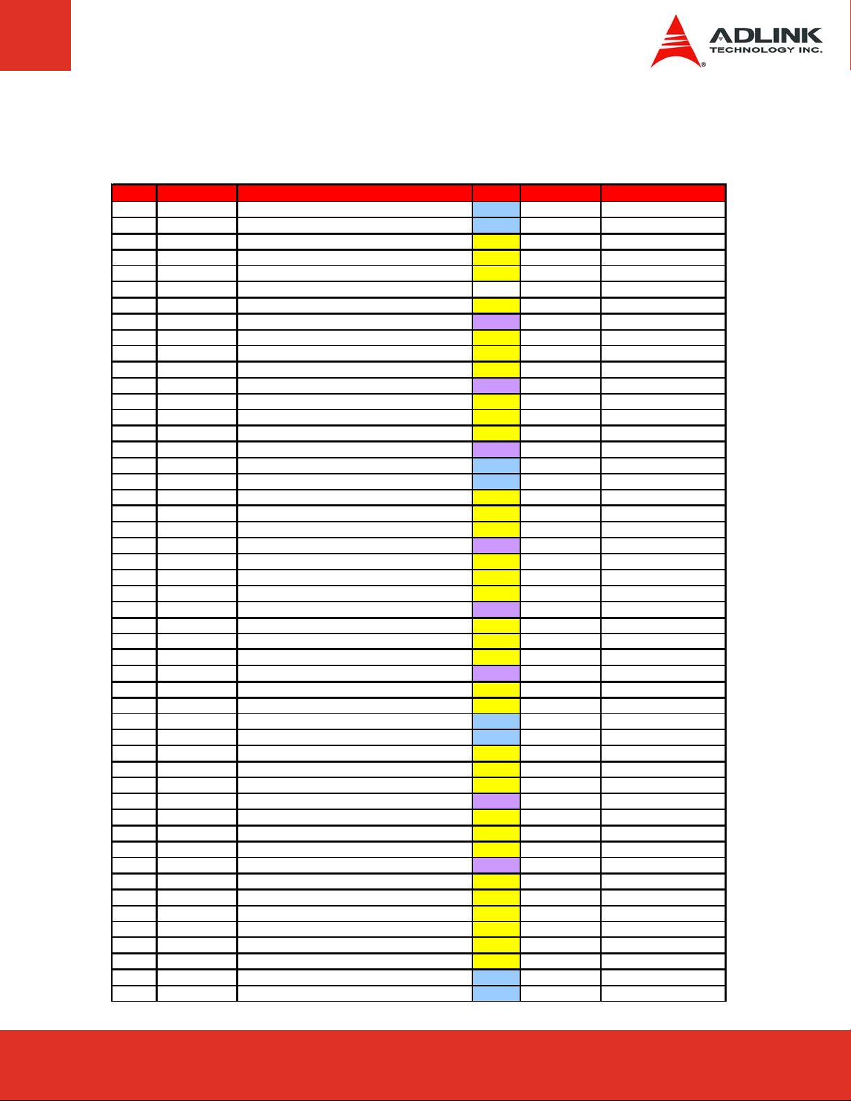
Pin Signal Pin Signal
51 5VCC 52 5VCC
53 PAR 54 SERR#
55 GPERR 56 RSV
57 PME# 58 USB259 LOCK# 60 DEVSEL#
61 TRDY# 62 USB363 IRDY# 64 STOP#
65 FRAME# 66 USB2+
67 GND 68 GND
69 AD16 70 CBE2#
71 AD17 72 USB3+
73 AD19 74 AD18
75 AD20 76 USB0N
77 AD22 78 AD21
79 AD23 80 USB181 AD24 82 CBE3#
83 5VCC 84 5VCC
85 AD25 86 AD26
87 AD28 88 USB0+
89 AD27 90 AD29
91 AD30 92 USB1+
93 PCIRST# 94 AD31
95 INTC# 96 INTD#
97 INTA# 98 INTB#
99 GND 100 GND
The 3V (3.3 V ±5%) is generated onboard. Pins may be used to power devices on the
carrier board up to a maximum load of 500 mA.
Do not connect the 3V pin to external 3.3V supply power.
ETX-CV User’s Manual Page 17
ETX-CV User’s Manual Page 17
Page 18
99 100
X2: ISA Bus
Pin Signal Pin Signal
1 GND 2 GND
3 SD14 4 SD15
5 SD13 6 MASTER#
7 SD12 8 DREQ7
9 SD11 10 DACK7#
11 SD10 12 DREQ6
13 SD9 14 DACK6#
15 SD8 16 DREQ5
17 MEMW# 18 DACK5#
19 MEMR# 20 DREQ0
21 LA17 22 DACK0#
23 LA18 24 IRQ14
25 LA19 26 IRQ15
27 LA20 28 IRQ12
29 LA21 30 IRQ11
31 LA22 32 IRQ10
33 LA23 34 IO16#
35 GND 36 GND
37 SBHE# 38 M16#
39 SA0 40 OSC
41 SA1 42 BALE
43 SA2 44 TC
45 SA3 46 DACK2#
47 SA4 48 IRQ3
49 SA5 50 IRQ4
X2
21
Pin Signal Pin Signal
51 5VCC 52 5VCC
53 SA6 54 IRQ5
55 SA7 56 IRQ6
57 SA8 58 IRQ7
59 SA9 60 SYSCLK
61 SA10 62 REFSH#
63 SA11 64 DREQ1
65 SA12 66 DACK1#
67 GND 68 GND
69 SA13 70 DREQ3
71 SA14 72 DACK3#
73 SA15 74 IOR#
75 SA16 76 IOW#
1
77 SA18 78 SA17
79 SA19 80 SMEMR#
81 IOCHRDY 82 AEN
83 5VCC 84 5VCC
85 SD0 86 SMEMW#
87 SD2 88 SD1
89 SD3 90 NOWS#
91 DREQ2 92 SD4
93 SD5 94 IRQ9
95 SD6 96 SD7
97 IOCHK# 98 RSTDRV
99 GND 100 GND
1
IRQ12 is reserved for a PS/2 mouse.
ETX-CV User’s ManualPage 18
Page 19
X3: CRT, LCD (LVDS), & Video
Pin Signal Pin Signal
1 GND 2 GND
3R 4B
5 HSY 6 G
7 VSY 8 DDCK
9 NC 10 DDDA
11 LCD16 12 LCD18
13 LCD17 14 LCD19
15 GND 16 GND
17 LCD13 18 LCD15
19 LCD12 20 LCD14
21 GND 22 GND
23 LCD8 24 LCD11
25 LCD9 26 LCD10
27 GND 28 GND
29 LCD4 30 LCD7
31 LCD5 32 LCD6
33 GND 34 GND
35 LCD1 36 LCD3
37 LCD0 38 LCD2
39 5VCC 40 5VCC
41 JILI_SDA 42 LTGO0
43 JILI_SCL 44 BLON#
45 NC 46 DIGON
47 COMP 48 Y
49 NC 50 C
99 100
X3
21
First LVDS Channel
Signal LVDS Signal
LCD0 Txout 0LCD1 Txout 0+
LCD2 Txout 1LCD3 Txout 1+
LCD4 Txout 2LCD5 Txout 2+
LCD6 Txclk LCD7 Txclk +
LCD8 Txout 3LCD9 Txout 3+
Second LVDS Channel
Signal LVDS Signal
LCD10 Txout 0LCD11 Txout 0+
LCD12 Txout 1LCD13 Txout 1+
LCD14 Txout 2LCD15 Txout 2+
LCD16 Txclk LCD17 Txclk +
LCD18 Txout 3LCD19 Txout 3+
ETX-CV User’s Manual Page 19
ETX-CV User’s Manual Page 19
Page 20

X3: COM1/2, LPT1, IrDA, Mouse, & Keyboard
X3
Pin Signal Pin
51 LPT/FLPY# 52 RESERVED
53 5VCC 54 GND
55 STB# 56 AFD#
57 RESERVED 58 PD7
59 IRRX 60 ERR#
61 IRTX 62 PD6
63 RXD2 64 INIT#
65 GND 66 GND
67 RTS2# 68 PD5
69 DTR2# 70 SLIN#
71 DCD2# 72 PD4
73 DSR2# 74 PD3
75 CTS2# 76 PD2
77 TXD2 78 PD1
79 RI2# 80 PD0
81 5VCC 82 5VCC
83 RXD1 84 ACK#
85 RTS1# 86 BUSY
87 DTR1# 88 PE
89 DCD1# 90 SLCT#
91 DSR1# 92 MSCLK
93 CTS1# 94 MSDAT
95 TXD1 96 KBCLK
97 RI1# 98 KBDAT
99 GND 100 GND
99 100
21
ETX-CV User’s ManualPage 20
Page 21
X4: IDE1, IDE2, Ethernet, & Miscellaneous
99 100
X4
21
Pin Signal Pin Signal
1 GND 2 GND
3 5V_SB 4 PWGIN
5 PS_ON 6 SPEAKER
7 PWRBTN# 8 BATT
9 KBINH 10 LILED#
11 RSMRST#
13 ROMKBCS#
15 EXT_PRG
1
2
12 ACTLED#
2
14 SPDLED#
16 I2CLK
3
17 5VCC 18 5VCC
19 OVCR# 20 NC
21 EXTSMI# 22 I2DAT
23 SMBCLK
3
24 SMBDATA
3
25 S_CS3# 26 SMBALRT#
27 S_CS1# 28 NC
29 S_A2 30 P_CS3#
31 S_A0 32 P_CS1#
33 GND 34 GND
35 PDIAG_S 36 P_A2
37 S_A1 38 P_A0
39 S_INTRQ 40 P_A1
41 BATLOW#
2
42 GPE1#
2
43 S_AK# 44 P_INTRQ
45 S_RDY 46 P_AK#
47 S_IOR# 48 P_RDY
49 5VCC 50 5VCC
Pin Signal Pin Signal
51 S_IOW# 52 P_IOR#
53 S_DRQ 54 P_IOW#
55 S_D15 56 P_DRQ
57 S_D0 58 P_D15
59 S_D14 60 P_D0
61 S_D1 62 P_D14
63 S_D13 64 P_D1
65 GND 66 GND
67 S_D2 68 P_D13
69 S_D12 70 P_D2
71 S_D3 72 P_D12
3
73 S_D11 74 P_D3
75 S_D4 76 P_D11
77 S_D10 78 P_D4
79 S_D5 80 P_D10
81 5VCC 82 5VCC
83 S_D9 84 P_D5
85 S_D6 86 P_D9
87 S_D8 88 P_D6
89 GPE2#
2
90 CBLID_P#
91 RXD# 92 P_D8
93 RXD 94 S_D7
95 TXD# 96 P_D7
97 TXD 98 HDRST#
99 GND 100 GND
1
May be affected by external circuitry to reset the power management logic of the ETX
module. Most designs do not use and pin is not connected.
2
Reserved, do not connect
3
See also: section 7.7 System Management Bus (I2C-compatible)
ETX-CV User’s Manual Page 21
ETX-CV User’s Manual Page 21
Page 22
6.4 Signal Descriptions
Pin Signal Description Type PU/PD Comment
1 GND Ground PWR - 2 GND Ground PWR - 3 PCICLK3 PCI Clock Slot 3 O-3, 3 - 4 PCICLK4 PCI Clock Slot 4 O-3, 3 - 5 GND Ground PWR - 6 GND Ground PWR - 7 PCICLK1 PCI Clock Slot 1 O-3, 3 - 8 PCICLK2 PCI Clock Slot 2 O-3, 3 - -
9 REQ3# PCI Bus Request 3 I-3,3 PU 8k2 3,3V 10 GNT3# PCI Bus Gra n t 3 O-3,3 - int. PU 20k 3,3V
11 GNT2# PCI Bus Gra n t 2 O-3,3 - int. PU 20k 3,3V
12 3V Power +3,3V PWR - 13 REQ2# PCI Bus Request 2 I-3,3 PU 8k2 3,3V 14 GNT1# PCI Bus Gra n t 1 O-3,3 - int. PU 20k 3,3V
15 REQ1# PCI Bus Request 1 I-3,3 PU 8k2 3,3V 16 3V Power +3,3V PWR - 17 GNT0# PCI Bus Gra n t 0 O-3,3 - int. PU 20k 3,3V
18 RSVD - NC - Reserved
19 5VCC Power +5V PWR - 20 5VCC Power +5V PWR - 21 SERIRQ Serial Interrupt Reqest IO-3,3 PU 8k2 3,3V 22 REQ0# PCI Bus Request 0 I-3,3 PU 8k2 3,3V 23 AD0 PCI Adress & Data Bu s line IO-3,3 24 3V Power +3,3V PWR - 25 AD1 PCI Adress & Data Bu s line IO-3,3 - 26 AD2 PCI Adress & Data Bu s line IO-3,3 - 27 AD4 PCI Adress & Data Bu s line IO-3,3 - 28 AD3 PCI Adress & Data Bu s line IO-3,3 - 29 AD6 PCI Adress & Data Bu s line IO-3,3 - 30 AD5 PCI Adress & Data Bu s line IO-3,3 - 31 CBE0# PCI Bus Command and Byte enables 0 IO-3,3 - 32 AD7 PCI Adress & Data Bu s line IO-3,3 - 33 AD8 PCI Adress & Data Bu s line IO-3,3 - 34 AD9 PCI Adress & Data Bu s line IO-3,3 - 35 GND Ground PWR - 36 GND Ground PWR - 37 AD10 PCI Adres s & Data Bu s lin e IO- 3,3 - 38 AUXAL Au xilia ry L ine Input Lef t I
39 AD11 PCI Adres s & Data Bu s lin e IO- 3,3 - 40 MIC Microphone Input I - 41 AD12 PCI Adres s & Data Bu s lin e IO- 3,3 - 42 AUXAR Auxiliary Line Input R ight I
43 AD13 PCI Adres s & Data Bu s lin e IO- 3,3 - 44 ASVCC Analog Supply of Sound Controller O-5 - 45 AD14 PCI Adres s & Data Bu s lin e IO- 3,3 - 46 SNDL Audio Out Left O - 47 AD15 PCI Adres s & Data Bu s lin e IO- 3,3 - 48 ASGND Analog Ground of Sound Controller P - 49 CBE1# PCI Bus Command and Byte enables 1 IO-3,3 - 50 SNDR Audio Out Right O - -
X1
ETX-CV User’s ManualPage 22
Page 23
Signal Descriptions (cont’d)
X1
Pin Signal Description Type PU/PD Comment
51 5VCC Power +5V PWR
52 5VCC Power +5V PWR
53 PAR PCI Bus Parity IO-3,3
54 SERR# PCI Bus System Error IO-3,3 PU 8k2 3,3V
55 GP ERR# PCI Bus Grant Erro r IO-3,3 PU 8k2 3,3 V
56 RSV - NC Reserved
57 PME# PCI Power Management Event IO-3,3 int. PU 20k 3,3V
58 USB2N USB Data- Port2 I/O - DP int. PD 15k
59 LOCK# PCI Bus Lock IO-3,3 PU 8k2 3,3V
60 DEVSEL# PCI Bus Device Select IO -3 ,3 PU 8k2 3,3V
61 TRDY# PIC Bus Target Ready IO-3,3 PU 8k2 3,3V
62 USB3N USB Data- Port3 I/O - DP int. PD 15k
63 IRDY# PCI Bus Initiator Ready IO-3,3 PU 8k2 3,3V
64 STOP# PCI Bus Stop IO-3,3 PU 8k2 3,3V
65 FRAME# P CI Bus Cycle Frame IO-3,3 PU 8k2 3,3V
66 USB2P USB Data+ Port2 I/O - DP int. PD 15k
67 GND Ground PWR
68 GND Ground PWR
69 AD16 PCI Adress & Data Bus line IO-3,3
70 CBE2# PCI Bus Command and Byte enables 2 IO-3,3
71 AD17 PCI Adress & Data Bus line IO-3,3
72 USB3P USB Data+ Port3 I/O - DP int. PD 15k
73 AD19 PCI Adress & Data Bus line IO-3,3
74 AD18 PCI Adress & Data Bus line IO-3,3
75 AD20 PCI Adress & Data Bus line IO-3,3
76 USB0N USB Data- Port0 I/O - DP int. PD 15k
77 AD22 PCI Adress & Data Bus line IO-3,3
78 AD21 PCI Adress & Data Bus line IO-3,3
79 AD23 PCI Adress & Data Bus line IO-3,3
80 USB1N USB Data- Port1 I/O - DP int. PD 15k
81 AD24 PCI Adress & Data Bus line IO-3,3
82 CBE3# PCI Bus Command and Byte enables 3 IO-3,3
83 5VCC Power +5V PWR
84 5VCC Power +5V PWR
85 AD25 PCI Adress & Data Bus line IO-3,3
86 AD26 PCI Adress & Data Bus line IO-3,3
87 AD28 PCI Adress & Data Bus line IO-3,3
88 USB0P USB Data+ Port0 I/O - DP int. PD 15k
89 AD27 PCI Adress & Data Bus line IO-3,3
90 AD29 PCI Adress & Data Bus line IO-3,3
91 AD30 PCI Adress & Data Bus line IO-3,3
92 USB1P USB Data+ Port1 I/O - DP int. PD 15k
93 PCIRST# PCI Bus Reset O-3,3
94 AD31 PCI Adress & Data Bus line IO-3,3
95 INTC# PCI BUS Interrupt Reauest C I-3,3 PU 8k2 3,3V
96 INTD# PCI BUS Interrupt Reauest D I-3,3 PU 8k2 3,3V
97 INTA# PCI BUS Interrupt Reauest A I-3,3 PU 8k2 3,3V
98 INTB# PCI BUS Interrupt Reauest B I-3,3 PU 8k2 3,3V
99 GND Ground PWR
100 GND Ground PWR
ETX-CV User’s Manual Page 23
ETX-CV User’s Manual Page 23
Page 24
Signal Descriptions (cont’d)
X2
Pin Signal Description Type PU/PD Comment
1 GND Ground PWR - -
2 GND Ground PWR - -
3 SD14 ISA Data Bus IO-5 PU 4k7 5V int. PU 50k 5V in
4 SD15 ISA Data Bus IO-5 PU 4k7 5V int. PU 50k 5V in
5 SD13 ISA Data Bus IO-5 PU 4k7 5V int. PU 50k 5V in
6 MASTER# ISA 16-Bit Master I-5 PU 330R 5V int. PU 50k 5V in
7 SD12 ISA Data Bus IO-5 PU 4k7 5V int. PU 50k 5V in
8 DREQ7 ISA DMA Request 7 I-5 PU 4k7 5V int. PD 50k
9 SD11 ISA Data Bus IO-5 PU 4k7 5V int. PU 50k 5V in
10 DACK7# ISA DMA Acknowledge 7 IO-5 PU 4k7 5V int. PU 50k 5V in
11 SD10 ISA Data Bus IO-5 PU 4k7 5V int. PU 50k 5V in
12 DREQ6 ISA DMA Request 6 I-5 PU 4k7 5V int. PD 50k
13 SD9 ISA Data Bus IO-5 PU 4k7 5V int. PU 50k 5V in
14 DACK6# ISA DMA Acknowledge 6 IO-5 PU 4k7 5V int. PU 50k 5V in
15 SD8 ISA Data Bus IO-5 PU 4k7 5V int. PU 50k 5V in
16 DREQ5 ISA DMA Request 5 I-5 PU 4k7 5V int. PD 50k
17 MEMW# ISA Memory Write IO-5 PU 4k7 5V int. PU 50k 5V in
18 DACK5# ISA DMA Acknowledge 5 IO-5 PU 4k7 5V int. PU 50k 5V in
19 MEMR# ISA Memory Read IO-5 PU 4k7 5V int. PU 50k 5V in
20 DREQ0 ISA DMA Request 0 I-5 PU 4k7 5V int. PD 50k
21 LA17 ISA Address Bus (SA17) O-5 PU 4k7 5V 22 DACK0# ISA DMA Acknowledge 0 IO-5 PU 4k7 5V int. PU 50k 5V in
23 LA18 ISA Address Bus (SA18) O-5 PU 4k7 5V 24 IRQ14 ISA Interrupt Request 14 / ROMChip Select IO-5 PU 4k7 5V int. PU 50k 5V in
25 LA19 ISA Address Bus (SA19) O-5 PU 4k7 5V 26 IRQ15 ISA Interrupt Request 15 IO-5 PU 4k7 5V int. PU 50k 5V in
27 LA20 ISA Address Bus (SA20) O-5 PU 4k7 5V 28 IRQ12 ISA Interrupt Request 12 IO-5 PU 4k7 5V int. PU 50k 5V in
29 LA21 ISA Address Bus (SA21) O-5 PU 4k7 5V 30 IRQ11 ISA Interrupt Request 11 IO-5 PU 4k7 5V int. PU 50k 5V in
31 LA22 ISA Address Bus (SA22) O-5 PU 4k7 5V 32 IRQ10 ISA Interrupt Request 10 IO-5 PU 4k7 5V int. PU 50k 5V in
33 LA23 ISA Address Bus (SA23) O-5 PU 4k7 5V
34 IO16# ISA 16-Bit I/O Access I-5 PU 330R 5V int. PU 50k 5V in
35 GND Ground PWR - 36 GND Ground PWR - 37 SBHE# ISA System Byte High Enable IO-5 PU 4k7 5V int. PU 50k 5V in
38 M16# ISA 16-Bit Memory Access IO-5 PU 330R 5V int. PU 50k 5V in
39 SA0 ISA Address Bus O-5 PU 4k7 5V 40 OSC ISA Oscillator (CLK_ISA14#) O-3,3 - 41 SA1 ISA Address Bus O-5 PU 4k7 5V 42 BALE ISA Buffer Address Latch Enable IO-5 PD 4k7 int. PU 50k 5V in
43 SA2 ISA Address Bus O-5 PU 4k7 5V
44 TC ISA Terminal Count IO-5 PD 4k7 int. PU 50k 5V in
45 SA3 ISA Address Bus O-5 PU 4k7 5V 46 DACK2# ISA DMA Acknowledge 2 IO-5 PU 4k7 5V int. PU 50k 5V in
47 SA4 ISA Address Bus O-5 PU 4k7 5V 48 IRQ3 ISA Interrupt Request 3 IO-5 PU 4k7 5V int. PU 50k 5V in
49 SA5 ISA Address Bus O-5 PU 4k7 5V 50 IRQ4 ISA Interrupt Request 4 IO-5 PU 4k7 5V int. PU 50k 5V in
ETX-CV User’s ManualPage 24
Page 25
Signal Descriptions (cont’d)
X2
Pin Signal Description Type PU/PD Comment
51 5VCC Power +5V PWR - 52 5VCC Power +5V PWR - 53 SA6 ISA Address Bus O-5 PU 4k7 5V 54 IRQ5 ISA Interrupt Request 5 IO-5 PU 4k7 5V int. PU 50k 5V in
55 SA7 ISA Address Bus O-5 PU 4k7 5V 56 IRQ6 ISA Interrupt Request 6 IO-5 PU 4k7 5V int. PU 50k 5V in
57 SA8 ISA Address Bus O-5 PU 4k7 5V 58 IRQ7 ISA Interrupt Request 7 IO-5 PU 4k7 5V int. PU 50k 5V in
59 SA9 ISA Address Bus O-5 PU 4k7 5V 60 SYSCLK ISA Bus Clock (CLK_SYS_ISA) O-3,3 - 61 SA10 ISA Address Bus O-5 PU 4k7 5V 62 REFSH# ISA System Refresh Control IO-5 PU 1k 5V int. PU 50k 5V in
63 SA11 ISA Address Bus O-5 PU 4k7 5V 64 DREQ1 ISA DMA Request 1 I-5 PU 4k7 5V int. PD 50k
65 SA12 ISA Address Bus O-5 PU 4k7 5V 66 DACK1# ISA DMA Acknowledge 1 IO-5 PU 4k7 5V int. PU 50k 5V in
67 GND Ground PWR - 68 GND Ground PWR - 69 SA13 ISA Address Bus O-5 PU 4k7 5V 70 DREQ3 ISA DMA Request 3 I-5 PU 4k7 5V int. PD 50k
71 SA14 ISA Address Bus O-5 PU 4k7 5V 72 DACK3# ISA DMA Acknowledge 3 IO-5 PU 4k7 5V int. PU 50k 5V in
73 SA15 ISA Address Bus O-5 PU 4k7 5V 74 IOR# ISA I/O Read IO-5 PU 4k7 5V int. PU 50k 5V in
75 SA16 ISA Address Bus O-5 PU 4k7 5V 76 IOW# ISA I/O Write IO-5 PU 4k7 5V int. PU 50k 5V in
77 SA18 ISA Address Bus O-5 PU 4k7 5V 78 SA17 ISA Address Bus O-5 PU 4k7 5V 79 SA19 ISA Address Bus O-5 PU 4k7 5V 80 SMEMR# ISA System Memory Read IO-5 PU 4k7 5V int. PU 50k 5V in
81 IOCHRDY ISA I/O Channel Ready IO-5 PU 1k 5V int. PU 50k 5V in
82 AEN ISA Address Enable IO -5 PD 47k int. PU 50k 5V in
83 5VCC Power +5V PWR - 84 5VCC Power +5V PWR - 85 SD0 ISA Data Bus IO-5 PU 4k7 5V int. PU 50k 5V in
86 SMEMW# ISA System Memory Write IO-5 PU 4k7 5V int. PU 50k 5V in
87 SD2 ISA Data Bus IO-5 PU 4k7 5V int. PU 50k 5V in
88 SD1 ISA Data Bus IO-5 PU 4k7 5V int. PU 50k 5V in
89 SD3 ISA Data Bus IO-5 PU 4k7 5V int. PU 50k 5V in
90 NOWS# ISA No Wait Staits I-5 PU 330R 5V int. PU 50k 5V in
91 DREQ2 ISA DMA Request 2 I-5 PU 4k7 5V int. PD 50k
92 SD4 ISA Data Bus IO-5 PU 4k7 5V int. PU 50k 5V in
93 SD5 ISA Data Bus IO-5 PU 4k7 5V int. PU 50k 5V in
94 IRQ9 ISA Interrupt Request 9 IO-5 PU 4k7 5V int. PU 50k 5V in
95 SD6 ISA Data Bus IO-5 PU 4k7 5V int. PU 50k 5V in
96 SD7 ISA Data Bus IO-5 PU 4k7 5V int. PU 50k 5V in
97 IOCHK# ISA I/O Channel Check I-5 PU 4k7 5V int. PU 50k 5V in
98 RSTDRV ISA Reset O-5 - 99 GND Ground PWR - -
100 GND Ground PWR - -
ETX-CV User’s Manual Page 25
ETX-CV User’s Manual Page 25
Page 26
Signal Descriptions (cont’d)
X3
Pin Signal Description Type PU/PD Comment
1 GND Ground PWR - -
2 GND Ground PWR - -
3 R Analog Video Out RGB - Red Channel OA PD 150R -
4 B Analog Video Out RGB - Blue Channel OA PD 150R -
5 HSY Horizontal Synchronization Pulse O-3,3 - -
6 G Analog Video Out RGB - Green Channel OA PD 150R -
7 VSY Vertical Synchronization Pulse O-3,3 - -
8 DDCK Display Data Channel Clock IO-5 PU 2k2 3,3V -
9 DETECT# Panel Hot-Plug Detection NC 10 DDDA Display Data Channel Data IO-5 PU 2k2 3,3V 11 LCD16 Second LVDS Channel Data Txclk - O - DP 12 LCD18 Second LVDS Channel Data Txout 3- O - DP 13 LCD17 Second LVDS Channel Data Txclk + O - DP 14 LCD19 Second LVDS Channel Data Txout 3+ O - DP 15 GND Ground PWR - 16 GND Ground PWR - 17 LCD13 Second LVDS Channel Data Txout 1+ O - DP 18 LCD15 Second LVDS Channel Data Txout 2+ O - DP 19 LCD12 Second LVDS Channel Data Txout 1- O - DP 20 LCD14 Second LVDS Channel Data Txout 2- O - DP 21 GND Ground PWR - 22 GND Ground PWR - 23 LCD8 First LVDS Channel Data Txout 3- O - DP 24 LCD11 Second LVDS Channel Data Txout 0+ O - DP - 25 LCD9 First LVDS Channel Data Txout 3+ O - DP 26 LCD10 Second LVDS Channel Data Txout 0- O - DP - 27 GND Ground PWR - 28 GND Ground PWR - 29 LCD4 First LVDS Channel Data Txout 2- O - DP - 30 LCD7 First LVDS Channel Data Txclk + O - DP - 31 LCD5 First LVDS Channel Data Txout 2+ O - DP - 32 LCD6 First LVDS Channel Data Txclk - O - DP - 33 GND Ground PWR - 34 GND Ground PWR - 35 LCD1 First LVDS Channel Data Txout 0+ O - DP - 36 LCD3 First LVDS Channel Data Txout 1+ O - DP - 37 LCD0 First LVDS Channel Data Txout 0- O - DP - 38 LCD2 First LVDS Channel Data Txout 1- O - DP - 39 5VCC Power +5V PWR - 40 5VCC Power +5V PWR - 41 JILI_DAT JILI I2C Data Signal IO-3,3 PU 10k 3,3V 42 LTGIO0 Display Backlight Control O-5 - 43 JILI_CLK JILI I2C Clock Signal IO-3,3 PU 10k 3,3V 44 BLON# Display Backlight On O-5 - 45 BIASON Display Contrast NC - 46 DIGON Display Power On O-5 - 47 COMP Composite Video / SCART Blue OA - 48 Y S-Video Luminance / SCART Red OA - 49 SYNC Composite Sync NC - 50 C S-Video Chrominance / SCART Green OA - -
NC on ETX-AT-N270-18
NC on ETX-AT-N270-18
NC on ETX-AT-N270-18
NC on ETX-AT-N270-18
NC on ETX-AT-N270-18
NC on ETX-AT-N270-18
NC on ETX-AT-N270-18
NC on ETX-AT-N270-18
NC on ETX-AT-N270-18
NC on ETX-AT-N270-18
ETX-CV User’s ManualPage 26
Page 27

Signal Descriptions (cont’d)
X3
Pin Signal Description Type PU/PD Comment
51 LPT | FLPY# LPT / Floppy Interface Select IO-3,3 PU 10k 3,3V 52 RSV - NC - 53 5VCC Power +5V PWR - 54 GND Ground PWR - 55 STB# | RSV LPT Strobe Signal O-5 - -
AFD# | DENSEL LPT Automat ic Feed / Flo ppy Densit y S elect
56
57 RSV - NC - 58 PD7 | RSV L PT Dat a Bus D7 IO -5 - 59 IRRX Infrared Receive I-5 - -
ERR# | HDSEL#
60
61 IRTX Infrared Transmit O-5 - 62 PD6 | RSV L PT Dat a Bus D6 IO -5 - 63 RXD2 Data Receive COM2 I-5 - 64 INIT# | DIR# LPT Initiate / Floppy Direction O-5 - 65 GND Ground PWR - 66 GND Ground PWR - 67 RTS2# Request to Send COM2 O-5 - 68 PD5 | RSV L PT Dat a Bus D5 IO -5 - 69 DTR2# Data Terminal Ready COM2 O-5 - -
SL IN# | STE P#
70
71 DCD2# Data Carrier Detect COM2 I-5 - -
PD 4 | DS K C HG #
72
73 DSR2# Data Set Ready COM2 I-5 - -
PD3 | RDATA#
74
75 CTS2 # Clear to Send COM2 I-5 - 76 PD2 | WP# LPT Data Bus D2 IO-5 - 77 TXD2 Data Transmit COM2 O-5 PU 4k7 5V 78 PD1 | TRK0# LPT Data Bus D1 IO-5 - 79 RI2# Ring Indicator COM2 I-5 - 80 PD0 | INDEX# LPT Data Bus D0 IO-5 - 81 5VCC Power +5V PWR - 82 5VCC Power +5V PWR - 83 RXD1# Data Receive COM1 I-5 - 84 ACK# | DRV LPT Acknowledge / Floppy Drive Select IO-5 - 85 RTS1# Request to Send COM1 O-5 PD 4k7 86 BUSY# | MOT LPT Busy / Floppy Mo tor Select IO-5 - 87 DTR1# Data Terminal Ready COM1 O-5 - 88 PE | WDATA# LPT Paper Emp ty / Floppy Raw Write Data IO-5 - 89 DCD1# Data Carrier Detect COM1 I-5 - 90
SLCT#|WGATE# LPT Power On / Floppy Write Enable IO-5 - -
91 DSR1# Data Set Ready COM1 I-5 - 92 MSCLK Mouse Clock O-5 PU 4k7 5V 93 CTS1 # Clear to Send COM1 I-5 - 94 MSDAT Mouse Data O-5 PU 4k7 5V 95 TXD1 Data Transmit COM1 O-5 PU 4k7 5V 96 KBCLK Keyboard Clock O -5 PU 4k7 5V 97 RI1# Ring Indicator COM1 I-5 - 98 KBDAT Ke yboard Data O-5 PU 4k7 5V 99 GND Ground PWR - -
100 GND Ground PWR - -
LPT Error / Flopp y Head Selec t IO-5 - -
LPT Select / Floppy Motor Step O-5 - -
LPT Data Bu s D4 IO-5 - -
LPT Data Bu s D3 IO-5 - -
O-5 - -
ETX-CV User’s Manual Page 27
ETX-CV User’s Manual Page 27
Page 28

Signal Descriptions (cont’d)
X4
Pin Signal Description Type PU/PD Comme nt
1GNDGround PWR - 2GNDGround PWR - 3 5V_SB Supply of internal suspend Circuit PWR - 4 PWGIN Po wer Good / Reset Input I-3,3 - 5 PS_ON Power Supply On O-5 PU 4k7 3,3VSB 6 SPEAKER Speaker Output O-5 PU 1k 5V 7 PWRBTN# Power Button I-5
8 BATT Battery Supply PWR - 9 KBINH Keyboard Inhibit Control Input I-5 PU 8k2 5V -
10 LILED Ethernet Link LED O-3,3 - 11 RSMRST# Resume Reset input I-3,3
12 ACTLED Ethernet Activity LED O-3,3 - 13 ROMKBCS# - NC - 14 SPDLED Ethernet Speed LED O-3,3 - 15 EXT_PRG - NC - 16 I2CLK I2C Bus Clock O-5 PU 10k 3,3V
17 5VCC Power +5V PWR - 18 5VCC Power +5V PWR - 19 OVCR# Over Current Detect for USB I-3,3 PU 4k7 3,3VSB 20 GPCS# - NC - 21 EXTSMI# System Management Interrupt Input I-3,3 PU 8k2 3,3V 22 I2DAT I2C Bus Data IO -5 PU 10k 3,3V 23 SMBCLK SM Bus Clock O-3,3 PU 2k2 3,3V 24 SMBDATA SM Bus Data IO-3,3 PU 2k2 3,3V 25 S_CS 3# S ec ondary IDE Chip Sel ect Cha nnel 1 O-3,3 - 26 SMBALERT SM Bus Alert I-3,3 PU 10k 3,3VSB 27 S_CS 1# S ec ondary IDE Chip Sel ect Cha nnel 0 O-3,3 - 28 DASP_S - I-3,3 PD 10k 29 S_A2 Secondary IDE Adress Bus O-3,3 - 30 P_CS3# Primary IDE Chip Select Channel 1 O-3,3 - 31 S_A0 Secondary IDE Adress Bus O-3,3 - 32 P_CS1# Primary IDE Chip Select Channel 0 O-3,3 - 33 GND Ground PWR - 34 GND Ground PWR - 35 PDIAG_S 80-conductor IDE cable Channel 1 I-3,3 - 36 P_A2 Primary IDE Adress Bus O-3,3 - 37 S_A1 Secondary IDE Adress Bus O-3,3 - 38 P_A0 Primary IDE Adress Bus O-3,3 - 39 S_INTRQ Secondary IDE Interrupt Request I-3,3 PD 10k 40 P_A1 Primary IDE Adress Bus O-3,3 - 41 BATLOW# Battery Low I-3,3 42 GPE1# - NC - 43 S_AK# Secondary IDE DMA Acknowledge O-3,3 - 44 P_INTRQ Primary IDE Interrupt Reqeuest I-3,3 PU 8k2 3,3V 45 S_RDY Secondary IDE Ready I-3,3 PU 4k7 3,3V 46 P_AK# Primary IDE DMA Acknowledge O-3, 3 - 47 S_IOR# Secondary IDE IO Read O-3,3 - 48 P_RDY Primary IDE Ready I-3,3 PU 4k7 3,3V 49 5VCC Power +5V PWR - 50 5VCC Power +5V PWR - -
PU 10k 3,3VSB
PU 20k 3,3VSB
-
-
ETX-CV User’s ManualPage 28
Page 29

Signal Descriptions (cont’d)
X4
Pin Signal Description Type PU/PD Comme nt
51 S_IOW# Secondary IDE IO Write O -3,3 - 52 P_IOR# Primary IDE IO Read O-3,3 - 53 S_DRQ Secondary IDE DMA Request I-3,3 - 54 P_IOW# Primary IDE IO Write O-3,3 - 55 S_D15 Secondary IDE Data Bus IO - 56 P_DRQ
57 S_D0 Secondary IDE Data Bus IO - 58 P_D15 Primary IDE Data Bus IO - 59 S_D14 Secondary IDE Data Bus IO - 60 P_D0 Primary IDE Data Bus IO - 61 S_D1 Secondary IDE Data Bus IO - 62 P_D14 Primary IDE Data Bus IO - 63 S_D13 Secondary IDE Data Bus IO - 64 P_D1 Primary IDE Data Bus IO - 65 GND Ground PWR - 66 GND Ground PWR - 67 S_D2 Secondary IDE Data Bus IO - 68 P_D13 Primary IDE Data Bus IO - 69 S_D12 Secondary IDE Data Bus IO - 70 P_D2 Primary IDE Data Bus IO - 71 S_D3 Secondary IDE Data Bus IO - 72 P_D12 Primary IDE Data Bus IO - 73 S_D11 Secondary IDE Data Bus IO - 74 P_D3 Primary IDE Data Bus IO - 75 S_D4 Secondary IDE Data Bus IO - 76 P_D11 Primary IDE Data Bus IO - 77 S_D10 Secondary IDE Data Bus IO - 78 P_D4 Primary IDE Data Bus IO - 79 S_D5 Secondary IDE Data Bus IO - 80 P_D10 Primary IDE Data Bus IO - 81 5VCC Power +5V PWR - 82 5VCC Power +5V PWR - 83 S_D9 Secondary IDE Data Bus IO - 84 P_D5 Primary IDE Data Bus IO - 85 S_D6 Secondary IDE Data Bus IO - 86 P_D9 Primary IDE Data Bus IO - 87 S_D8 Secondary IDE Data Bus IO - 88 P_D6 Primary IDE Data Bus IO - 89 GPE2# - NC - 90 CBLID_P# 80-conductor IDE cable Channel 0 I-3,3 - 91 RXD# Ethernet Receive Differential Signal ( RXD-) I - DP - 92 P_D8 Primary IDE Data Bus IO - 93 RXD
94 S_D7 Secondary IDE Data Bus IO - 95 TXD# Ethernet Transmit Differential Signal (TXD-) O -DP - 96 P_D7 Primary IDE Data Bus IO - in t. PD 11k5
97 TXD Ethernet Transmit Differential Signal (TXD+) O -DP - 98 HDRST# Hard Drive Reset O-3,3 - 99 GND Ground PWR - -
100 GND Ground PWR - -
Primary IDE DMA Request
Ethernet Receive Differentia l Signal ( RXD+)
I-3,3 - -
I - DP - -
ETX-CV User’s Manual Page 29
ETX-CV User’s Manual Page 29
Page 30

Signal Descriptions (cont’d)
Signal Type Legend
IO-2,5 Bi-directional 2,5 V Input/Output
IO-3,3 Bi-directional 3,3 V Input/Output
IO-5 Bi-directional 5 V Input/Output
I-3,3 3,3 V Input
I-5 5 V Input
O-2,5 2,5 V Output
O-3,3 3,3 V Output
O-5 5 V Output
IO Input/Output
OA Analog Output
I/O - DP Differential Pair Input/Output
O - DP Differential Pair Output
I - DP Differential Pair Input
PWR Power or Ground
PU Pull-Up Resistor
PD Pull-Down Resistor
NC Not Connected / Reserved
ETX-CV User’s ManualPage 30
Page 31

7 System Resources
7.1 System Memory Map
Address Range (decimal) Address Range (hex) Size Description
(4GB-2MB) FFE00000 - FFFFFFFF 2 MB High BIOS Area
(4GB-18MB)-(4GB-17MB-1) FEE00000 - FEEFFFFF 1 MB FSB Interrupt Memory Space
(4GB-20MB)-(4GB-19MB-1) FEC00000 – FECFFFFF 1 MB APIC Configuration Space
960 K - 1024 K F0000 - FFFFF 64 KB System BIOS Area
896 K - 960 K E0000 - EFFFF 64 KB Extended System BIOS Area
768 K - 896 K C0000 - DFFFF 128 KB PCI expansion ROM area
640 K - 768 K A0000 - BFFFF 128 KB Video Buffer & SMM space
0 K - 640 K 00000 - 9FFFF 640 KB DOS Area
C0000 - CEFFF: Onboard VGA BIOS
CF000 - D0FFF: PXE option ROM when
onboard LAN boot ROM is enabled.
ETX-CV User’s Manual Page 31
ETX-CV User’s Manual Page 31
Page 32

7.2 I/O Address Map
Address (hex) Size Description
0000 – 001F 32 bytes DMA controller
0020 – 0021 2 bytes Interrupt controller
0024 – 0025 2 bytes Interrupt controller
0028 – 0029 2 bytes Interrupt controller
002C – 002D 2 bytes Interrupt controller
002E - 002F 2 bytes LPC SIO
0030 – 0031 2 bytes Interrupt controller
0034 – 0035 2 bytes Interrupt controller
0038 – 0039 2 bytes Interrupt controller
003C – 003D 2 bytes Interrupt controller
0040 – 0043 4 bytes Counter/Timer
0048 – 004B 4 bytes Counter/Timer
004E – 004F 2 bytes TPM configuration port
0050 – 0053 4 bytes Counter/Timer
0060 1 byte Keyboard controller
0061 1 byte NMI, speaker control
0063 1 byte NMI controller
0064 1 byte Keyboard controller
0065 1 byte NMI controller
0067 1 byte NMI controller
0070 – 0071 2 bytes Real time clock controller
0072 – 0073 2 bytes Real time clock controller
0074 – 0075 2 bytes Real time clock controller
0076 – 0077 2 bytes Real time clock controller
0080 – 0091 18 bytes DMA controller
0092 1 bytes Reset Generator
0093 – 009F 13 bytes DMA controller
00A0 – 00A1 2 bytes Interrupt controller
00A4 – 00A5 2 bytes Interrupt controller
00A8 – 00A9 2 bytes Interrupt controller
00AC – 00AD 2 bytes Interrupt controller
00B0 – 00B1 2 bytes Interrupt controller
00B2 – 00B3 2 bytes Power Management
00B4 – 00B5 2 bytes Interrupt controller
00B8 – 00B9 2 bytes Interrupt controller
00BC – 00BD 2 bytes Interrupt controller
00C0 – 00DF 32 bytes DMA controller
00F0 – 00FF 16 bytes Numeric processor
0170 – 0177 8 bytes Secondary IDE controller
01F0 – 01F7 8 bytes Primary IDE controller
0274 – 0277 4 bytes ISA PnP read port
0278 – 027F 8 bytes LPT2
0290 – 029F 16 bytes Onboard Sensor index(0x295)/data port (0x296)
02E8 – 02EF 8 bytes COM4/Video
ETX-CV User’s ManualPage 32
Page 33

I/O Address Map (cont’d)
Address (hex) Size Description
02F8 – 02FF 8 bytes COM2
0376 – 0377 2 bytes Secondary IDE controller
0378 – 037F 8 bytes LPT1
03B0 – 03BB 12 bytes Video (monochrome)
03BC – 03BF 4 bytes LPT3
03C0 – 03DF 32 bytes Video (VGA†)
03E8 – 03EF 8 bytes COM3
03F0 – 03F5, 03F7 7 bytes Diskette controller
03F6 – 03F7 2 bytes Primary IDE controller
03F8 – 03FF 8 bytes COM1
0400 – 041F 32 bytes Onboard SMBus control registers
0480 – 04BF 64 bytes GPIO control registers
04D0 – 04D1 2 bytes Edge/level triggered PIC
0800 – 087F 128 bytes ACPI control registers
0A79 – 0A79 1 bytes ISA PnP read data Port
0CF8 – 0CFF* 8 bytes PCI configuration registers
0CF9** 1 byte Reset control register
04700 – 0470F 16 bytes TPM control registers
0C4802-0C49F 32Byte USB Host Controller
0C800-0C81F 32Byte USB Host Controller
0C880-0C89F 32Byte USB Host Controller
0CC00-0CC1F 32Byte USB Host Controller
0CC80-CC87 8Byte Video
0D480-0D48F 16Byte PCI IDE Controller
0D800-0D803 4Byte PCI IDE Controller
0DC00-0DC03 4Byte PCI IDE Controller
0DC80-ODC87 8Byte PCI IDE Controller
0FFA0-0FFAF 16Byte Serial ATA Storage Controller
* DWORD access only
** Byte access only
ETX-CV User’s Manual Page 33
ETX-CV User’s Manual Page 33
Page 34

7.3 Interrupt Request (IRQ) Lines
PIC Mode
IRQ# Typical Interrupt Resource Connected to Pin Available
0 Counter 0 N/A No
1 Keyboard controller N/A No
2 Cascade interrupt from slave PIC N/A No
3 Serial Port 2 (COM2) / PCI IRQ3 via SERIRQ Note (1)
4 Serial Port 1 (COM1) / PCI IRQ4 via SERIRQ Note (1)
5 Parallel Port 2 (LPT2) / PCI IRQ5 via SERIRQ Note (1)
6 Floppy Drive Controller IRQ6 via SERIRQ No
7 Parallel Port 1 (LPT1) / PCI IRQ7 via SERIRQ, Note (1)
8 Real-time clock N/A No
9 SCI / PCI IRQ9 via SERIRQ Note (1)
10 PCI IRQ10 via SERIRQ Note (1)
11 PCI IRQ11 via SERIRQ Note (1)
12 PS/2 Mouse / PCI IRQ12 via SERIRQ Note (1)
13 Math Processor N/A No
14 Primary IDE controller / PCI IRQ14 via SERIRQ Note (1)
15 Secondary IDE controller / PCI IRQ15 via SERIRQ Note (1)
(1) These IRQs can be used for PCI devices when onboard device is disabled.
APIC Mode
IRQ# Typical Interrupt Resource Connected to Pin Available
0 Counter 0 N/A No
1 Keyboard controller N/A No
2 Cascade interrupt from slave PIC N/A No
3 Serial Port 2 (COM2) / PC IRQ3 via SERIRQ Note (1)
4 Serial Port 1 (COM1) / PCI IRQ4 via SERIRQ Note (1)
5 Parallel Port 2 (LPT2) / PCI IRQ5 via SERIRQ Note (1)
6 Floppy Drive Controller IRQ6 via SERIRQ No
7 Parallel Port 1 (LPT1) / PCI / ISA IRQ7 via SERIRQ Note (1)
8 Real-time clock N/A No
9 SCI / PCI IRQ9 via SERIRQ Note (1),
10 PCI IRQ10 via SERIRQ Note (1)
11 PCI IRQ11 via SERIRQ Note (1)
12 PS/2 Mouse / PCI IRQ12 via SERIRQ Note (1)
13 Math Processor N/A No
14 Primary IDE controller / PCI IRQ14 via SERIRQ Note (1)
ETX-CV User’s ManualPage 34
Page 35

APIC Mode (cont’d)
IRQ# Typical Interrupt Resource Connected to Pin Available
15 Secondary IDE controller / PCI IRQ15 via SERIRQ Note (1)
16 N/A PCI Slot INT A, USB, VGA controller, Yes
17 N/A PCI Slot INT B, USB Yes
18 N/A PCI Slot INT C Yes
19 N/A PCI Slot INT D, USB controller Yes
20 N/A No
21 N/A No
22 N/A No
23 N/A EHCI, USB No
(1) These IRQs can be used for PCI devices when an onboard device is disabled.
7.4 PCI Configuration Space Map
Audio controller, IDE controller
Bus # Device # Function # Routing Description
00h 00h 00h N/A Intel 945 GSE GMCH Host-Hub Interface Bridge
00h 02h 00h Internal Intel Integrated Graphics Device
00h 02h 01h Internal Intel Integrated Graphics Device (Function 1)
00h 1Bh 00h Internal High Definition Audio controller
00h 1Ch 00h Internal Intel ICH Express Root port
00h 1Dh 00h Internal Intel USB UHCI Controller 1
00h 1Dh 01h Internal Intel USB UHCI Controller 2
00h 1Dh 02h Internal Intel USB UHCI Controller 3
00h 1Dh 03h Internal Intel USB UHCI Controller 4
00h 1Dh 07h Internal Intel USB EHCI Controller
00h 1Eh 00h N/A Intel Hub Interface to PCI Bridge
00h 1Fh 00h N/A Intel LPC Interface Bridge
00h 1Fh 01h Internal Intel IDE Controller
00h 1Fh 02h Internal Intel SATA controller
00h 1Fh 03h Internal Intel SMBus Controller
01h 00h 00h onboard JMB368 PCI IDE controller
02h 07h 00h onboard ITE8888 PCI to ISA Bridge
02h 08h 00h onboard Onboard LAN controller
ETX-CV User’s Manual Page 35
ETX-CV User’s Manual Page 35
Page 36

7.5 PCI Interrupt Routing Map
PIRQ A B C D E F G H
INT Line INTA INTB INTC INTD
VGA X
UHCI 1 X
UHCI 2 X
UHCI 3 X
UHCI 4 X
EHCI X
SATA X
SMBus X
Audio X
PCI Slot1 INTA INTB INTC INTD
PCI Slot2 INTB INTC INTD INTA
PCI Slot3 INTC INTD INTA INTB
PCI Slot4 INTD INTA INTB INTC
LAN INTA
7.6 System Management Bus (I2C-compatible)
Internally the SMB bus and I2C bus are one and the same. The ICH7-M Southbridge supports
SMBDAT and SMBCLK lines that are I2C-compatible.
The X4 connector has pins for both the I2C and SMB bus. Both are connected to the same
internal bus: the SMB bus. It is advisable to always connect external I2C devices to the I2C pins
and SMB devices to the SMB pins to ensure compatibility with other modules that might support
two internal busses (a separate I2C and SMB bus).
Address Function Device
2Eh Super I/O Read/Write SIO
A0h Memory SPD SO-DIMM
D2h Clock Generator CLK GEN
ETX-CV User’s ManualPage 36
Page 37

8 BIOS Setup Utility
The following chapter describes basic navigation for the AMI EFI BIOS setup utility.
8.1 Starting the BIOS
To enter the setup screen, follow these steps:
1. Power on the motherboard
2. Press the < Delete > key on your keyboard when you see the following text prompt:
< Press DEL or Delete to run Setup >
3. After you press the < Delete > key, the main BIOS setup menu displays. You can
access the other setup screens from the main BIOS setup menu, such as Chipset and
Power menus.
In most cases, the < Delete > key is used to invoke the setup screen. There are
several cases that use other keys, such as < F1 >, < F2 >, and so on.
ETX-CV User’s Manual Page 37
ETX-CV User’s Manual Page 37
Page 38

8.1.1 Main Setup Menu
The main BIOS setup menu is the first screen that you can navigate. Each main BIOS setup
menu option is described in this user’s guide.
The Main BIOS setup menu screen has two main frames. The left frame displays all the options
that can be configured. “Grayed” options cannot be configured, “Blue” options can be.
The right frame displays the key legend. Above the key legend is an area reserved for a text
message. When an option is selected in the left frame, it is highlighted in white. Often a text
message will accompany it.
ETX-CV User’s ManualPage 38
Page 39

8.1.2 Navigation
The BIOS setup/utility uses a key-based navigation system called hot keys. Most of the BIOS
setup utility hot keys can be used at any time during the setup navigation process.
These keys include < F1 >, < F10 >, < Enter >, < ESC >, < Arrow > keys, and so on.
There is a hot key legend located in the right frame on most setup screens.
Navigation
Left/Right The Left and Right < Arrow > keys allow you to select a setup screen.
For example: Main screen, Advanced screen, Chipset screen, and so on.
Up/Down The Up and Down < Arrow > keys allow you to select a setup item or sub-screen.
+- Plus/Minus The Plus and Minus < Arrow > keys allow you to change the field value of a particular
setup item.
For example: Date and Time.
Tab The < Tab > key allows you to select setup fields.
ETX-CV User’s Manual Page 39
ETX-CV User’s Manual Page 39
Page 40

Hot Key Description
Enter The < Enter > key allows you to display or change the setup option listed for a particular setup
item. The < Enter > key can also allow you to display the setup sub-screens.
F1 The < F1 > key allows you to display the General Help screen. Press the < F1 > key to open the
General Help screen.
F2 The < F2 > key is the previous values key. It is not displayed on the key legend by default. To set the
previous values settings of the BIOS, press the < F2 > key on your keyboard. It is located on the upper
row of a standard 101 keyboard. The previous values settings allow the motherboard to boot up with the
least amount of options set. This can lessen the probability of conflicting settings.
Press the < Enter > key to load previous values. You can also use the < Arrow > key to select
Cancel and then press the < Enter > key to abort this function and return to the previous screen.
F3 The < F3 > key is the optimized defaults key. To set the optimized defaults settings of the BIOS, press
the < F3 > key on your keyboard. It is located on the upper row of a standard 101 keyboard. The
previous values settings allow the motherboard to boot up with the least amount of options set. This can
lessen the probability of conflicting settings.
Press the < Enter > key to load optimized defaults. You can also use the < Arrow > key to select
Cancel and then press the < Enter > key to abort this function and return to the previous screen.
ETX-CV User’s ManualPage 40
Page 41

F4 The < F4 > key allows you to save any changes you have made and exit Setup. Press the < F4 > key
to save your changes. The following screen will appear:
Press the < Enter > key to save the configuration and exit. You can also use the < Arrow > key
to select Cancel and then press the < Enter > key to abort this function and return to the previous screen.
ESC The < Esc > key allows you to discard any changes you have made and exit the Setup. Press the
< Esc > key to exit the setup without saving your changes. The following screen will appear:
Press the < Enter > key to discard changes and exit. You can also use the < Arrow > key to select
Cancel and then press the < Enter > key to abort this function and return to the previous screen.
ETX-CV User’s Manual Page 41
ETX-CV User’s Manual Page 41
Page 42

8.2 Main Setup
When you first enter the Setup Utility, you will enter the Main setup screen. You can always return
to the Main setup screen by selecting the Main tab. There are two Main Setup options. They are
described in this section. The Main BIOS Setup screen is shown below.
8.2.1 System Time/System Date
Use this option to change the system time and date. Highlight System Time or System Date using
the < Arrow > keys. Enter new values using the keyboard. Press the < Tab > key or the
< Arrow > keys to move between fields. The date must be entered in MM/DD/YY format. The
time is entered in HH:MM:SS format.
The time is in 24-hour format. For example, 5:30 A.M. appears as 05:30:00, and 5:30 P.M.
as 17:30:00.
8.2.2 System Time/System Date
This sub menu reports detailed board information.
ETX-CV User’s ManualPage 42
Page 43

8.3 Advanced BIOS Setup
Select the Advanced tab from the setup screen to enter the Advanced BIOS Setup screen. You
can select any of the items in the left frame of the screen, such as SuperIO Configuration, to go
to the sub menu for that item. You can display an Advanced BIOS Setup option by highlighting it
using the < Arrow > keys. The Advanced BIOS Setup screen is shown below.
The sub menus are described on the following pages.
Setting incorrect or conflicting values in Advanced BIOS Setup may cause system
malfunctions.
ETX-CV User’s Manual Page 43
ETX-CV User’s Manual Page 43
Page 44

8.3.1 PCI Subsystem Settings
You can use this screen to select options for the PCI Subsystem Configuration Settings. Use the
up and down < Arrow > keys to select an item. Use the < + > and < - > keys to change the value
of the selected option. A description of the selected item appears on the right side of the screen.
The settings are described on this page. The screen is shown below.
PCI Latency Timer
Value to be programmed into PCI Latency Timer Register.
ETX-CV User’s ManualPage 44
Page 45

8.3.2 ACPI Settings
You can use this screen to select options for the ACPI configuration settings. Use the up and
down < Arrow > keys to select an item. Use the < + > and < - > keys to change the value of
the selected option. A description of the selected item appears on the right side of the screen.
The settings are described on the following pages. An example of the ACPI Settings screen is
shown below.
Enable APIC Auto Configuration
BIOS ACPI Auto Configuration. Set this value to Enabled/Disabled.
Enable Hibernation
System ability to Hibernate (OS/S4 Sleep State). Set this value to Enabled/Disabled.
ETX-CV User’s Manual Page 45
ETX-CV User’s Manual Page 45
Page 46

ACPI Sleep State
S1 only (CPU Stop Clock)
CPU Stop Clock - Under this setting the system enters a low power state instead of being
completely shut off. This allows the computer system to boot up in a few seconds.
S3 only (Suspend)
Suspend to RAM - Under this setting the system enters a low power state instead of being
completely shut off. This allows the computer system to boot up in a few seconds.
Emulation AT/ ATX
Select Emulation AT or ATX function. If this option is set to Emulation AT, BIOS will report no
suspends functions to ACPI OS. In Windows XP, it will cause the OS to show a shutdown
message during system shutdown.
ETX-CV User’s ManualPage 46
Page 47

8.3.3 Trusted Computing
You can use this screen to select options for the Trusted Computing settings. Use the up and
down < Arrow > keys to select an item. Use the < + > and < - > keys to change the value of
the selected option. A description of the selected item appears on the right side of the screen.
The settings are described on the following pages. An example of the Trusted Computing screen
is shown below.
Security Device Support
Enables or Disables BIOS support for security device. O.S. will not show Security Device. TCG
EFI protocol and INT1A interface will not be available.
ETX-CV User’s Manual Page 47
ETX-CV User’s Manual Page 47
Page 48

8.3.4 CPU Configuration
You can use this screen to select options for the CPU Configuration Settings. Use the up and
down < Arrow > keys to select an item. Use the < + > and < - > keys to change the value of
the selected option. A description of the selected item appears on the right side of the screen.
The settings are described on the following pages. An example of the CPU Configuration screen
is shown below.
Hyper-Threading Technology
This option enables/disables Intel® Hyper-Threading Technology.
Execute Disable Bit Capability
This is an Intel hardware-based security feature that can prevent certain classes of malicious
buffer overflow attacks when combined with a supporting OS (Windows Server 2003 SP1,
Windows XP SP2, SuSE Linux 9.2, RedHat Enterprise 3 Update 3.) . Set this value to Enabled/
Disabled.
Limit CPUID Maximum
When the computer is boots, the operating system executes its CPUID instruction to identify the
processor and its capabilities. Before it can do so, it must first query the processor to find out the
highest input value the CPUID recognizes. This determines the kind of basic information CPUID
can provide the operating system. This option allows you to circumvent problems with older
operating systems.
ETX-CV User’s ManualPage 48
Page 49

When Enabled, the processor will limit the maximum CPUID input value to 03h when queried,
even if the processor supports a higher CPUID input value. When Disabled, the processor will
return the actual maximum CPUID input value of the processor when queried.
8.3.5 Thermal Configuration
You can use this screen to select options for the Thermal Configuration settings. Use the up and
down < Arrow > keys to select an item. Use the < + > and < - > keys to change the value of
the selected option. A description of the selected item appears on the right side of the screen.
The settings are described on the following pages. An example of the Thermal Configuration
screen is shown below.
ETX-CV User’s Manual Page 49
ETX-CV User’s Manual Page 49
Page 50

Platform Thermal
DTS SMM
Enabled ACPI thermal management uses DTS SMM mechanism to obtain CPU temperature
values.
CPU Temperature
Display current CPU temperature.
Critical Trip Point
This value controls the temperature of the ACPI Critical Trip Point - the point in which the OS will
shut the system off. NOTE: 100C is the Plan of Record (POR) for all Intel mobile processors.
Passive Trip Point
This value controls the temperature of the ACPI Passive Trip Point - the point in which the OS will
begin throttling the processor.
ETX-CV User’s ManualPage 50
Page 51

8.3.6 IDE Configuration
You can use this screen to select options for the IDE Configuration settings. Use the up and down
< Arrow > keys to select an item. Use the < + > and < - > keys to change the value of the
selected option. A description of the selected item appears on the right side of the screen. The
settings are described on the following pages. An example of the IDE Configuration screen is
shown below.
SATA Controller
Enabled/Disable SATA Controller
Configure SATA as
Select a configuration IDE/AHCI for SATA Controller.
ETX-CV User’s Manual Page 51
ETX-CV User’s Manual Page 51
Page 52

Configure SATA as “AHCI”
Port0/1 Speed Limit
Select Port0/1 AHCI Speed Limit.
SATA Port 0/1
Enable or Disable SATA Port 0/1.
SATA Port 0/1 Hot Plug
Designates this port 0/1 as hot pluggable.
ETX-CV User’s ManualPage 52
Page 53

8.3.7 USB Configuration
Legacy USB Support
Enables legacy USB support. Auto option disables legacy support if no USB devices are
connected. Disable option will keep USB devices available only for EFI applications. Set this
value to Enabled/Disabled/Auto.
EHCI Hand-off
This is a workaround for OS without EHCI hand-off support. The EHCI ownership change should
be claimed by EHCI driver. Set this value to Enabled/Disabled.
USB transfer time-out
The time-out value for control, bulk, and interrupt transfers.Set this value to 1 sec / 5 sec / 10 sec
/ 20 sec.
Device reset time-out
USB mass storage device start unit command time-out. Set this value to 10 sec / 20 sec / 30 sec
/ 40 sec.
Device power-up delay
Maximum time the device will take before it properly reports itself to the host controller. 'Auto'
uses default value: for a root port it is 100 ms, for a hub port the delay is taken from hub
descriptor. Set this value to Auto/Manual.
ETX-CV User’s Manual Page 53
ETX-CV User’s Manual Page 53
Page 54

8.3.8 W83627DHG Super IO Configuration
You can use this screen to select options for the Super IO settings. Use the up and down < Arrow
> keys to select an item. Use the < + > and < - > keys to change the value of the selected option.
The settings are described on the following pages. The screen is shown below.
Serial Port 0,1 Configuration
Set Parameters of Serial Port 0, 1 (COM 1/2). Set this value to Enabled/Disabled.
Change Settings
This option specifies the base I/O port address and interrupt request address of Serial Port 0, 1
(COM 1/2). Options shown below.
ETX-CV User’s ManualPage 54
Page 55

Parallel Port
Set Parameters of Parallel Port. Set this value to Enable/Disable.
Change Settings
This option specifies the base I/O port address and interrupt request address of parallel port.
Options shown below.
Device Mode
Change the printer port mode.
ETX-CV User’s Manual Page 55
ETX-CV User’s Manual Page 55
Page 56

8.3.9 H/W Monitor
Use this screen to check system health status.
ETX-CV User’s ManualPage 56
Page 57

8.3.10 Serial Port Console Redirection
Console Redirection
Set this value to enable/disable console redirection.
Console Redirection Settings
The settings specify how the host computer and the remote computer (which the user is using)
will exchange data. Both computers should have the same or compatible settings.
ETX-CV User’s Manual Page 57
ETX-CV User’s Manual Page 57
Page 58

Terminal Type
VT100+ is the preferred terminal type for out-of-band management. Configuration options:
VT100, VT100+, VT-UTF8 , ANSI.
Bits per second
Select the bits per second you want the serial port to use for console redirection. The options are
115200, 57600, 38400, 19200, 9600.
Data Bits
Select the data bits you want the serial port to use for console redirection. Set this value to 7 / 8.
Parity
Set this option to select Parity for console redirection. The settings for this value are None, Even,
Odd, Mark, Space.
Stop Bits
Stop bits indicate the end of a serial data packet. (A start bit indicates the beginning). The
standard setting is 1 stop bit. Communication with slow devices may require more than 1 stop bit.
Set this value to 1 and 2.
Flow Control
Set this option to select Flow Control for console redirection. The settings for this value are None,
Hardware RTS/CTS.
VT-UTF8 Combo Key Support
Enable VT-UTF8 Combination Key Support for ANSI/VT100 terminals.
Recorder Mode
Enabled this mode, only text will be sent. This is to capture terminal data.Set this value to
Enabled/Disabled.
Resolution 100x31
Set this option to extended terminal resolution. Set this value to Enabled/Disabled.
Legacy OS Redirection
On Legacy OS, the number of rows and columns supported redirection. Set this value to 80x24 /
80x25.
ETX-CV User’s ManualPage 58
Page 59

Putty KeyPad
Select Function Key and KeyPad on Putty.
Redirection After BIOS POST
The Settings specify if BootLoader is selected than Legacy console redirection is disabled before
booting to Legacy OS. Default value is Always Enable which means Legacy console Redirection
is enabled for Legacy OS.
ETX-CV User’s Manual Page 59
ETX-CV User’s Manual Page 59
Page 60

8.3.11 PPM Configuration
EIST
It’s allow the clock speed of the processor to be dynamically changed.
Set this value to Enable/Disable.
C-States
Enable or Disable C2 and above. Set this value to Enable/Disable.
ETX-CV User’s ManualPage 60
Page 61

8.4 Chipset Configuration
Select the Chipset tab from the setup screen to enter the Chipset BIOS Setup screen. You can
select any of Chipset BIOS Setup options by highlighting it using the < Arrow > keys. The Chipset
BIOS Setup screen is shown below.
ETX-CV User’s Manual Page 61
ETX-CV User’s Manual Page 61
Page 62

8.4.1 Host Bridge
IGFX- Type – Boot Type
Select the boot display device. Set this value to CRT, LFP, CRT+LFP.
LCD Panel Type
When LVDS is selected from Boot Display Device, this option allows you to select resolution
settings as below:
Active LFP
Select the boot display device.
ETX-CV User’s ManualPage 62
Page 63

8.4.2 South Bridge
TPT Device
Enable/Disable Intel IO Controller Hub Device.
ETX-CV User’s Manual Page 63
ETX-CV User’s Manual Page 63
Page 64

Azalia Controller
The audio controller. Set this value to Disable/HD Auto.
UHCI #1-2 Controller
The UHCI controller. Set this value to Enabled/Disabled/Auto.
USB2.0 Controller
The EHCI controller. Set this value to EnabledDisabled.
SMBus Controller
The SMBus controller. Set this value to Enabled/Disabled.
PCI Express Ports Configuration
The PCI Express Ports in the chipset. Configuration options: Enabled, Disabled.
Restore AC Power Loss
Select AC power state when power is re-applied after a power failure.
ETX-CV User’s ManualPage 64
Page 65

8.5 Boot Setup
Select the Boot tab from the setup screen to enter the Boot BIOS Setup screen. You can select
any of the items in the left frame of the screen, such as Boot Device Priority, to go to the sub
menu for that item. You can display an Boot BIOS Setup option by highlighting it using the <
Arrow > keys. The Boot Settings screen is shown below:
Bootup Num-Lock
Set this value to allow the Number Lock setting to be modified during boot up.
Off - This option does not enable the keyboard Number Lock automatically. To use the 10-keys
on the keyboard, press the Number Lock key located on the upper left-hand corner of the 10-key
pad. The Number Lock LED on the keyboard will light up when the Number Lock is engaged.
On - Set this value to allow the Number Lock on the keyboard to be enabled automatically when the
computer system is boot up. This allows the immediate use of 10-keys numeric keypad located on
the right side of the keyboard. To confirm this, the Number Lock LED light on the keyboard will be lit.
Quiet Boot
Disabled - Set this value to allow the computer system to display the POST messages.
Enabled - Set this value to allow the computer system to display the OEM logo.
Fast Boot
Disabled - Set this value to allow the BIOS to perform all POST tests.
Enabled - Set this value to allow the BIOS to skip certain POST tests to boot faster.
ETX-CV User’s Manual Page 65
ETX-CV User’s Manual Page 65
Page 66

8.5.1 CSM Parameters
Launch CSM
This option controls if CSM will be launched.
Boot Option Filter
This option controls what devices system can boot to.
ETX-CV User’s ManualPage 66
Page 67

Launch PXE OpROM policy
This Controls the execution of UEFI and Legacy PXE OpROM.
Launch storage OpROM
This Controls the execution of UEFI and Legacy PXE OpROM.
Launch video OpROM policy
This Controls the execution of UEFI and Legacy PXE OpROM.
Other PCI device ROM
For PCI devices other than Network, Mass storage or Video defines which OpROM to launch.
ETX-CV User’s Manual Page 67
ETX-CV User’s Manual Page 67
Page 68

8.6 Security Setup
Administrator/User Password
If only the administrator’s password is set, then this only limits access to setup and is only asked
for when entering setup.
If only the user’s password is set, then this is a power on password and must be entered to boot
or enter setup. In setup the user will have administrator rights.
ETX-CV User’s ManualPage 68
Page 69

8.7 Save & Exit
Save Changes and Exit
When you have completed the system configuration changes, select this option to save changes
and continue booting the system. New configuration parameters will take effect after the next
system restart.
Discard Changes and Exit
Select this option to quit Setup without saving changes to the system configuration and continue
booting.
Save Changes and Reset
Reset the system after saving the changes.
Discard Changes and Reset
Reset system setup without saving any changes.
Save Options
Save changes made so far to any of the setup options.
ETX-CV User’s Manual Page 69
ETX-CV User’s Manual Page 69
Page 70

Save Changes
When you have completed the system configuration changes, select this option to save your
system configuration and continue. For some of the options it required to reset the system to take
effect. Select YES to Save Changes and continue.
Discard Changes
Discard any unsaved changes
Restore Defaults
Restore standard default values for all the setup options.
Save as User Defaults
Save the changes made so far as User Defaults.
Restore User Defaults
Restore the User Defaults to all the setup options.
ETX-CV User’s ManualPage 70
Page 71

9 BIOS Checkpoints, Beep Codes
This section of this document lists checkpoints and beep codes generated by AMIBIOS. The
checkpoints defined in this document are inherent to the AMIBIOS generic core, and do not
include any chipset or board specific checkpoint definitions.
Checkpoints and Beep Codes Definition
A checkpoint is either a byte or word value output to I/O port 80h. The BIOS outputs checkpoints
throughout bootblock and Power-On Self Test (POST) to indicate the task the system is currently
executing. Checkpoints are very useful for debugging problems that occur during the preboot process.
Beep codes are used by the BIOS to indicate a serious or fatal error. They are used when an error
occurs before the system video has been initialized, and generated by the system board speaker.
Viewing BIOS Checkpoints
Viewing all checkpoints generated by the BIOS requires a checkpoint card, also referred to as a
“POST Card” or “POST Diagnostic Card”. These are PCI add-in cards that show the value of I/O
port 80h on a LED display.
Some computers display checkpoints in the bottom right corner of the screen during POST. This
display method is limited, since it only displays checkpoints that occur after the video card has
been activated.
Keep in mind that not all computers using AMIBIOS enable this feature. In most cases, a
checkpoint card is the best tool for viewing AMIBIOS checkpoints.
ETX-CV User’s Manual Page 71
ETX-CV User’s Manual Page 71
Page 72

9.1 Status Code Ranges
Status Code Range Description
0x01 – 0x0F SEC Status Codes & Errors
0x10 – 0x2F PEI execution up to and including memory detection
0x30 – 0x4F PEI execution after memory detection
0x50 – 0x5F PEI errors
0x60 – 0xCF DXE execution up to BDS
0xD0 – 0xDF DXE errors
0xE0 – 0xE8 S3 Resume (PEI)
0xE9 – 0xEF S3 Resume errors (PEI)
0xF0 – 0xF8 Recovery (PEI)
0xF9 – 0xFF Recovery errors (PEI)
9.2 Standard Status Codes
SEC Status Codes
Status Code Description
0x0 Not used
Progress Codes
0x1 Power on. Reset type detection (soft/hard).
0x2 AP initialization before microcode loading
0x3 North Bridge initialization before microcode loading
0x4 South Bridge initialization before microcode loading
0x5 OEM initialization before microcode loading
0x6 Microcode loading
0x7 AP initialization after microcode loading
0x8 North Bridge initialization after microcode loading
0x9 South Bridge initialization after microcode loading
0xA OEM initialization after microcode loading
0xB Cache initialization
SEC Error Codes
0xC – 0xDReserved for future AMI SEC error codes
0xE Microcode not found
0xF Microcode not loaded
SEC Beep Codes
None.
ETX-CV User’s ManualPage 72
Page 73

PEI Status Codes
Status Code Description
0x0 Not used
Progress Codes
0x10 PEI Core is started
0x11 Pre-memory CPU initialization is started
0x12 Pre-memory CPU initialization (CPU module specific)
0x13 Pre-memory CPU initialization (CPU module specific)
0x14 Pre-memory CPU initialization (CPU module specific)
0x15 Pre-memory North Bridge initialization is started
0x16 Pre-Memory North Bridge initialization (North Bridge module specific)
0x17 Pre-Memory North Bridge initialization (North Bridge module specific)
0x18 Pre-Memory North Bridge initialization (North Bridge module specific)
0x19 Pre-memory South Bridge initialization is started
0x1A Pre-memory South Bridge initialization (South Bridge module specific)
0x1B Pre-memory South Bridge initialization (South Bridge module specific)
0x1C Pre-memory South Bridge initialization (South Bridge module specific)
0x1D – 0x2A OEM pre-memory initialization codes
0x2B Memory initialization. Serial Presence Detect (SPD) data reading
0x2C Memory initialization. Memory presence detection
0x2D Memory initialization. Programming memory timing information
0x2E Memory initialization. Configuring memory
0x2F Memory initialization (other).
0x30 Reserved for ASL (see ASL Status Codes section below)
0x31 Memory Installed
0x32 CPU post-memory initialization is started
0x33 CPU post-memory initialization. Cache initialization
0x34 CPU post-memory initialization. Application Processor(s) (AP) initialization
0x35 CPU post-memory initialization. Boot Strap Processor (BSP) selection
0x36 CPU post-memory initialization. System Management Mode (SMM) initialization
0x37 Post-Memory North Bridge initialization is started
0x38 Post-Memory North Bridge initialization (North Bridge module specific)
0x39 Post-Memory North Bridge initialization (North Bridge module specific)
0x3A Post-Memory North Bridge initialization (North Bridge module specific)
0x3B Post-Memory South Bridge initialization is started
0x3C Post-Memory South Bridge initialization (South Bridge module specific)
0x3D Post-Memory South Bridge initialization (South Bridge module specific)
0x3E Post-Memory South Bridge initialization (South Bridge module specific)
0x3F-0x4E OEM post memory initialization codes
0x4F DXE IPL is started
ETX-CV User’s Manual Page 73
ETX-CV User’s Manual Page 73
Page 74

PEI Status Codes (cont’d)
PEI Error Codes
0x50 Memory initialization error. Invalid memory type or incompatible memory speed
0x51 Memory initialization error. SPD reading has failed
0x52 Memory initialization error. Invalid memory size or memory modules do not match.
0x53 Memory initialization error. No usable memory detected
0x54 Unspecified memory initialization error.
0x55 Memory not installed
0x56 Invalid CPU type or Speed
0x57 CPU mismatch
0x58 CPU self test failed or possible CPU cache error
0x59 CPU micro-code is not found or micro-code update is failed
0x5A Internal CPU error
0x5B reset PPI is not available
0x5C-0x5F Reserved for future AMI error codes
S3 Resume Progress Codes
0xE0 S3 Resume is stared (S3 Resume PPI is called by the DXE IPL)
0xE1 S3 Boot Script execution
0xE2 Video repost
0xE3 OS S3 wake vector call
0xE4-0xE7 Reserved for future AMI progress codes
0xE0 S3 Resume is stared (S3 Resume PPI is called by the DXE IPL)
S3 Resume Error Codes
0xE8 S3 Resume Failed in PEI
0xE9 S3 Resume PPI not Found
0xEA S3 Resume Boot Script Error
0xEB S3 OS Wake Error
0xEC-0xEF Reserved for future AMI error codes
Recovery Progress Codes
0xF0 Recovery condition triggered by firmware (Auto recovery)
0xF1 Recovery condition triggered by user (Forced recovery)
0xF2 Recovery process started
0xF3 Recovery firmware image is found
0xF4 Recovery firmware image is loaded
0xF5-0xF7 Reserved for future AMI progress codes
Recovery Error Codes
0xF8 Recovery PPI is not available
0xF9 Recovery capsule is not found
0xFA Invalid recovery capsule
0xFB – 0xFF Reserved for future AMI error codes
ETX-CV User’s ManualPage 74
Page 75

PEI Beep Codes
# of Beeps Description
1 Memory not Installed
1 Memory was installed twice (InstallPeiMemory routine in PEI Core called twice)
2 Recovery started
3 DXEIPL was not found
3 DXE Core Firmware Volume was not found
7 Reset PPI is not available
4 Recovery failed
4 S3 Resume failed
DXE Status Codes
Status Code Description
0x60 DXE Core is started
0x61 NVRAM initialization
0x62 Installation of the South Bridge Runtime Services
0x63 CPU DXE initialization is started
0x64 CPU DXE initialization (CPU module specific)
0x65 CPU DXE initialization (CPU module specific)
0x66 CPU DXE initialization (CPU module specific)
0x67 CPU DXE initialization (CPU module specific)
0x68 PCI host bridge initialization
0x69 North Bridge DXE initialization is started
0x6A North Bridge DXE SMM initialization is started
0x6B North Bridge DXE initialization (North Bridge module specific)
0x6C North Bridge DXE initialization (North Bridge module specific)
0x6D North Bridge DXE initialization (North Bridge module specific)
0x6E North Bridge DXE initialization (North Bridge module specific)
0x6F North Bridge DXE initialization (North Bridge module specific)
0x70 South Bridge DXE initialization is started
0x71 South Bridge DXE SMM initialization is started
0x72 South Bridge devices initialization
0x73 South Bridge DXE Initialization (South Bridge module specific)
0x74 South Bridge DXE Initialization (South Bridge module specific)
0x75 South Bridge DXE Initialization (South Bridge module specific)
0x76 South Bridge DXE Initialization (South Bridge module specific)
0x77 South Bridge DXE Initialization (South Bridge module specific)
0x78 ACPI module initialization
0x79 CSM initialization
0x7A – 0x7F Reserved for future AMI DXE codes
0x80 – 0x8F OEM DXE initialization codes
0x90 Boot Device Selection (BDS) phase is started
0x91 Driver connecting is started
ETX-CV User’s Manual Page 75
ETX-CV User’s Manual Page 75
Page 76

DXE Status Codes (cont’d)
Status Code Description
0x92 PCI Bus initialization is started
0x93 PCI Bus Hot Plug Controller Initialization
0x94 PCI Bus Enumeration
0x95 PCI Bus Request Resources
0x96 PCI Bus Assign Resources
0x97 Console Output devices connect
0x98 Console input devices connect
0x99 Super IO Initialization
0x9A USB initialization is started
0x9B USB Reset
0x9C USB Detect
0x9D USB Enable
0x9E – 0x9F Reserved for future AMI codes
0xA0 IDE initialization is started
0xA1 IDE Reset
0xA2 IDE Detect
0xA3 IDE Enable
0xA4 SCSI initialization is started
0xA5 SCSI Reset
0xA6 SCSI Detect
0xA7 SCSI Enable
0xA8 Setup Verifying Password
0xA9 Start of Setup
0xAA Reserved for ASL (see ASL Status Codes section below)
0xAB Setup Input Wait
0xAC Reserved for ASL (see ASL Status Codes section below)
0xAD Ready To Boot event
0xAE Legacy Boot event
0xAF Exit Boot Services event
0xB0 Runtime Set Virtual Address MAP Begin
0xB1 Runtime Set Virtual Address MAP End
0xB2 Legacy Option ROM Initialization
0xB3 System Reset
0xB4 USB hot plug
0xB5 PCI bus hot plug
0xB6 Clean-up of NVRAM
0xB7 Configuration Reset (reset of NVRAM settings)
0xB8 – 0xBF Reserved for future AMI codes
0xC0 – 0xCF OEM BDS initialization codes
ETX-CV User’s ManualPage 76
Page 77

DXE Status Codes (cont’d)
DXE Error Codes
0xD0 CPU initialization error
0xD1 North Bridge initialization error
0xD2 South Bridge initialization error
0xD3 Some of the Architectural Protocols are not available
0xD4 PCI resource allocation error. Out of Resources
0xD5 No Space for Legacy Option ROM
0xD6 No Console Output Devices are found
0xD7 No Console Input Devices are found
0xD8 Invalid password
0xD9 Error loading Boot Option (LoadImage returned error)
0xDA Boot Option is failed (StartImage returned error)
0xDB Flash update is failed
0xDC Reset protocol is not available
DXE Beep Codes
# of Beeps Description
4 Some of the Architectural Protocols are not available
5 No Console Output Devices are found
5 No Console Input Devices are found
1 Invalid password
6 Flash update is failed
7 Reset protocol is not available
8 Platform PCI resource requirements cannot be met
ACPI/ASL Status Codes
Status Code Description
0x01 System is entering S1 sleep state
0x02 System is entering S2 sleep state
0x03 System is entering S3 sleep state
0x04 System is entering S4 sleep state
0x05 System is entering S5 sleep state
0x10 System is waking up from the S1 sleep state
0x20 System is waking up from the S2 sleep state
0x30 System is waking up from the S3 sleep state
0x40 System is waking up from the S4 sleep state
0xAC System has transitioned into ACPI mode. Interrupt controller is in PIC mode.
0xAA System has transitioned into ACPI mode. Interrupt controller is in APIC mode.
ETX-CV User’s Manual Page 77
ETX-CV User’s Manual Page 77
Page 78

9.3 OEM-Reserved Status Code Ranges
Status Code Description
0x5 OEM SEC initialization before microcode loading
0xA OEM SEC initialization after microcode loading
0x1D – 0x2A OEM pre-memory initialization codes
0x3F – 0x4E OEM PEI post memory initialization codes
0x80 – 0x8F OEM DXE initialization codes
0xC0 – 0xCF OEM BDS initialization codes
ETX-CV User’s ManualPage 78
Page 79

Appendix A: Connectors and Mounting
A.1 Carrier Board ETX Connecter Heights (Hirose FX8/FX8C Receptacles)
For different stacking heights, the receptacles for ETX carrier boards are available in two heights,
3 mm and 9.5 mm. When 3 mm receptacles are chosen, the carrier board should be free of
components.
FX8-100S-SV
100-pin board-to-board connector for
3 mm board stacking
This connector can be used with :
- 3 mm through-hole standoffs (SMT type)
- 3 mm threaded standoffs (DIP type)
FX8C-100S-SV5
100-pin board-to-board connector for
9.5 mm board stacking
This connector can be used with :
- 9.5 mm through-hole standoffs (SMT type)
- 9.5 mm threaded standoffs (DIP type)
FX8C/FX8 Common Spec
f Current capacity 0.4 A per pin
f Rated voltage 100 V AC
f Insulation resistance 100 M or greater @ 250 V DC
f Withstand voltage 300 V AC r.m.s.
f Contact resistance 45 m or less @ 100 mA DC
f Insulation PPS resin (Light brown, UL94V-0)
f Contacts phosphor bronze (gold plated contacts and leads)
ETX-CV User’s Manual Page 79
ETX-CV User’s Manual Page 79
Page 80

A.3 Mounting Procedures
There are several standard ways to mount an ETX board with heatspreader on a carrier board.
ETX boards may be mounted with 9.5 mm ETX connectors on the carrier board or standard 3
mm connectors. There are also two different types of heatspreaders to choose from:
heatspreaders with threaded standoffs which require inserting screws from under the carrier, or
top mounting heatspreaders using through-hole heatspreader standoffs and threaded carrier
board standoffs.
Top Mounting
3 mm Hirose FX8-100S-SV
Carrier Board Connectors
M2.5: 16 mm
with spring/washer
Heatspreader
6 mm through-hole
standoffs
ETX Module
Carrier
3 mm threaded
standoff (DIP)
Top Mounting
9.5 mm Hirose FX8C-100S-SV5
Carrier Board Connectors
M2.5: 14 mm
with spring/washer
Bottom Mounting
3 mm Hirose FX8-100S-SV
Carrier Board Connectors
Heatspreader
6 mm threaded
standoffs
ETX Module
3 mm through-hole
standoff (SMT )
M2.5: 16 mm
with spring/w ash er
Carrier
Bottom Mounting
9.5 mm Hirose FX8C-100 S-SV5
Carrier Board Connectors
Heatspreader
6 mm threaded
standoffs
ETX Module
6 mm through-hole
standoffs
9.5 mm threaded
standoff (DIP )
Heatspreader
ETX Module
Carrier
9.5 mm through-hole
standoff (SMT )
Carrier
M2.5: 16 mm
with spring/washer
ETX-CV User’s ManualPage 80
Page 81

A.4 Standoff Types - Carrier Board
For different mounting procedures there are different standoffs available for the carrier board.
Note that threaded standoffs are both DIP and SMT type and the through-hole types are all SMT
type. Other types not listed can be made available upon request.
33-72000-0030
C0.2
33-72011-0030
C0.3
33-72007-9P50
3 mm through-hole standoff (SMT type)
for HTS-EAT-B with 3 mm Hirose carrier
board connectors
3 mm threaded standoff (DIP type)
for HTS-EAT-BT with 3 mm Hirose carrier
board connectors
C0.5
9.5 mm through-hole standoff (SMT type)
for HTS-EAT-B with 9.5 mm Hirose
33-72011-9P50
C0.2
C0.2
9.5 mm threaded standoff (DIP type)
carrier board connectors
for HTS-EAT-BT with 9.5 mm Hirose
C0.5
C0.3
ETX-CV User’s Manual Page 81
ETX-CV User’s Manual Page 81
carrier board connectors
Page 82

Important Safety Instructions
For user safety, please read and follow all instructions, warnings, cautions, and notes marked
in this manual and on the associated equipment before handling/operating the equipment.
f Read these safety instructions carefully.
f Keep this user’s manual for future reference.
f Read the specifications section of this manual for detailed information on the operating
environment of this equipment.
f When installing/mounting or uninstalling/removing equipment:
- Turn off power and unplug any power cords/cables.
f To avoid electrical shock and/or damage to equipment:
- Keep equipment away from water or liquid sources;
- Keep equipment away from high heat or high humidity;
- Keep equipment properly ventilated (do not block or cover ventilation openings);
- Make sure to use recommended voltage and power source settings;
- Always install and operate equipment near an easily accessible electrical socket-outlet;
- Secure the power cord (do not place any object on/over the power cord);
- Only install/attach and operate equipment on stable surfaces and/or recommended
mountings; and,
- If the equipment will not be used for long periods of time, turn off and unplug the
equipment from its power source.
f Never attempt to fix the equipment. Equipment should only be serviced by qualified
personnel.
f A Lithium-type battery may be provided for uninterrupted, backup or emergency power.
Risk of explosion if battery is replaced by an incorrect type. Dispose of used batteries
according to the instructions.
ETX-CV User’s ManualPage 82
Page 83

f Equipment must be serviced by authorized technicians when:
- The power cord or plug is damaged;
- Liquid has penetrated the equipment;
- It has been exposed to high humidity/moisture;
- It is not functioning or does not function according to the user’s manual;
- It has been dropped and/or damaged; and/or,
- It has an obvious sign of breakage.
ETX-CV User’s Manual Page 83
ETX-CV User’s Manual Page 83
Page 84

Getting Service
Contact us should you require any service or assistance.
ADLINK Technology, Inc.
Address: 9F, No.166 Jian Yi Road, Zhonghe District
New Taipei City 235, Taiwan
ᄅקؑխࡉ৬ԫሁ 166 ᇆ 9 ᑔ
Tel: +886-2-8226-5877
Fax: +886-2-8226-5717
Email: service@adlinktech.com
Ampro ADLINK Technology, Inc.
Address: 5215 Hellyer Avenue, #110
San Jose, CA 95138, USA
Tel: +1-408-360-0200
Toll Free: +1-800-966-5200 (USA only)
Fax: +1-408-360-0222
Email: info@adlinktech.com
ADLINK Technology (China) Co., Ltd.
Address: Ϟ⍋Ꮦ⌺ϰᮄᓴ∳催⾥ᡔು㢇䏃 300 ো(201203)
300 Fang Chun Rd., Zhangjiang Hi-Tech Park
Pudong New Area, Shanghai, 201203 China
Tel: +86-21-5132-8988
Fax: +86-21-5132-3588
Email: market@adlinktech.com
ADLINK Technology Beijing
Address: ࣫ҀᏖ⍋⎔Ϟഄϰ䏃 1 োⲜ߯ࡼ E ᑻ 801 ᅸ(100085)
Rm. 801, Power Creative E, No. 1 Shang Di East Rd.
Beijing, 100085 China
Tel: +86-10-5885-8666
Fax: +86-10-5885-8626
Email: market@adlinktech.com
ADLINK Technology Shenzhen
Address: ⏅ഇᏖቅ⾥ᡔು催ᮄϗ䘧᭄ᄫᡔᴃು
A1 2 ὐ C (518057)
2F, C Block, Bldg. A1, Cyber-Tech Zone, Gao Xin Ave. Sec. 7
High-Tech Industrial Park S., Shenzhen, 518054 China
Tel: +86-755-2643-4858
Fax: +86-755-2664-6353
Email: market@adlinktech.com
LiPPERT ADLINK Technology GmbH
Address: Hans-Thoma-Strasse 11, D-68163
Mannheim, Germany
Tel: +49-621-43214-0
Fax: +49-621 43214-30
Email: emea@adlinktech.com
ETX-CV User’s ManualPage 84
Page 85

ADLINK Technology, Inc. (French Liaison Office)
Address: 6 allée de Londres, Immeuble Ceylan
91940 Les Ulis, France
Tel: +33 (0) 1 60 12 35 66
Fax: +33 (0) 1 60 12 35 66
Email: france@adlinktech.com
ADLINK Technology Japan Corporation
Address: ͱ101-0045 ᵅҀ䛑ҷ⬄⼲⬄䤯ފ⬎ 3-7-4
⼲⬄ 374 ɛɳ 4F
KANDA374 Bldg. 4F, 3-7-4 Kanda Kajicho,
Chiyoda-ku, Tokyo 101-0045, Japan
Tel: +81-3-4455-3722
Fax: +81-3-5209-6013
Email: japan@adlinktech.com
ADLINK Technology, Inc. (Korean Liaison Office)
Address: 137-881 昢殾柢 昢爎割 昢爎堆嵢 326, 802 (昢爎壟, 微汾瘶捒娯)
802, Mointer B/D, 326 Seocho-daero, Seocho-Gu,
Seoul 137-881, Korea
Tel: +82-2-2057-0565
Fax: +82-2-2057-0563
Email: korea@adlinktech.com
ADLINK Technology Singapore Pte. Ltd.
Address: 84 Genting Lane #07-02A, Cityneon Design Centre
Singapore 349584
Tel: +65-6844-2261
Fax: +65-6844-2263
Email: singapore@adlinktech.com
ADLINK Technology Singapore Pte. Ltd. (Indian Liaison Office)
Address: #50-56, First Floor, Spearhead Towers
Margosa Main Road (between 16th/17th Cross)
Malleswaram, Bangalore - 560 055, India
Tel: +91-80-65605817, +91-80-42246107
Fax: +91-80-23464606
Email: india@adlinktech.com
ADLINK Technology, Inc. (Israeli Liaison Office)
Address: 27 Maskit St., Corex Building
PO Box 12777
Herzliya 4673300, Israel
Tel: +972-54-632-5251
Fax: +972-77-208-0230
Email: israel@adlinktech.com
ADLINK Technology, Inc. (UK Liaison Office)
Tel: +44 774 010 59 65
Email: UK@adlinktech.com
ETX-CV User’s Manual Page 85
ETX-CV User’s Manual Page 85
Page 86

 Loading...