

Page 1
ETX-BT
User’s Manual
Manual Revision: 1.01
Revision Date: May 7, 2015
Part Number: 50-1J059-1010
Page 2

Revision History
Revision Description Date By
1.00 Initial release 2015-03-18 JC
1.01 Correct SPI Boot Device Switch settings 2015-05-07 JC
Page 2
Page 3

Preface
Copyright 2015 ADLINK Technology, Inc.
This document contains proprietary information protected by copyright. All rights are reserved. No
part of this manual may be reproduced by any mechanical, electronic, or other means in any form
without prior written permission of the manufacturer.
Disclaimer
The information in this document is subject to change without prior notice in order to improve
reliability, design, and function and does not represent a commitment on the part of the
manufacturer. In no event will the manufacturer be liable for direct, indirect, special, incidental, or
consequential damages arising out of the use or inability to use the product or documentation,
even if advised of the possibility of such damages.
Environmental Responsibility
ADLINK is committed to fulfill its social responsibility to global environmental preservation through
compliance with the European Union's Restriction of Hazardous Substances (RoHS) directive and
Waste Electrical and Electronic Equipment (WEEE) directive. Environmental protection is a top
priority for ADLINK. We have enforced measures to ensure that our products, manufacturing
processes, components, and raw materials have as little impact on the environment as possible.
When products are at their end of life, our customers are encouraged to dispose of them in
accordance with the product disposal and/or recovery programs prescribed by their nation or
company.
Trademarks
Product names mentioned herein are used for identification purposes only and may be trademarks
and/or registered trademarks of their respective companies.
Page 3
Page 4

Table of Contents
Revision History..................................................................................2
Preface..............................................................................................3
1 Introduction....................................................................................7
1.1 Description..................................................................................................................... 7
2 Specifications .................................................................................8
2.1 General .......................................................................................................................... 8
2.2 Video.............................................................................................................................. 9
2.3 Audio.............................................................................................................................. 9
2.4 Ethernet ....................................................................................................................... 10
2.5 Multi I/O and Storage ................................................................................................... 10
2.6 Super I/O...................................................................................................................... 10
2.7 SEMA Board Controller................................................................................................ 11
2.8 Power........................................................................................................................... 12
2.9 Mechanical and Environmental.................................................................................... 12
2.10 Operating Systems Support..................................................................................... 12
3 Functional Diagram........................................................................13
4 Mechanical Dimensions..................................................................14
5 Pinouts and Signal Descriptions......................................................15
5.1 X1: PCI Bus, USB, Audio............................................................................................. 15
5.2 X2: ISA......................................................................................................................... 18
5.3 X3: LVDS, Serial, Parallel, KB, MS .............................................................................. 21
5.4 X4: IDE 1, IDE 2, Ethernet, Miscellaneous................................................................... 24
6 Module Interfaces ..........................................................................27
6.1 Connector, Switch and LED Locations......................................................................... 27
Page 4
6.2 40-pin Multipurpose Connector.................................................................................... 29
6.3 Status LEDs................................................................................................................. 30
6.4 XDP Debug Header ..................................................................................................... 31
6.5 DP Connector .............................................................................................................. 32
6.5.1 Display Mode Selection ................................................................................................... 32
6.5.2 Power Output Modification for HDMI ............................................................................... 32
6.6 Fan Connector ............................................................................................................. 33
6.7 GbE Connector ............................................................................................................ 34
Page 5

6.8 SW1: SPI Boot Device Selection.................................................................................. 35
6.9 SW2: BIOS Setup Defaults RESET Button.................................................................. 35
6.10 SW4: PCI Interrupt Routing Select............................................................................... 37
6.11 SW3: PCI Voltage Level Selection ............................................................................... 37
7 SEMA (Smart Embedded Mana gement Agent)....................................38
7.1 Board Specific SEMA Functions .................................................................................. 39
7.1.1 Voltages........................................................................................................................... 39
7.1.2 Main Current.................................................................................................................... 39
7.1.3 BMC Status...................................................................................................................... 40
7.1.4 Exception Codes.............................................................................................................. 41
7.1.5 BMC Flags....................................................................................................................... 42
8 System Resources.........................................................................43
8.1 System Memory Map................................................................................................... 43
8.2 I/O Map........................................................................................................................ 43
8.3 Interrupt Request (IRQ) Lines...................................................................................... 44
8.3.1 PIC Mode......................................................................................................................... 44
8.3.2 APIC Mode ...................................................................................................................... 45
8.4 PCI Configuration Space Map...................................................................................... 46
8.5 PCI Interrupt Routing Map ........................................................................................... 47
8.6 SMBus Address Table ................................................................................................. 48
8.7 I2C Address Table........................................................................................................ 48
9 BIOS Setup...................................................................................49
9.1 Menu Structure ............................................................................................................ 49
9.2 Main............................................................................................................................. 50
9.2.1 System Information.......................................................................................................... 50
9.2.2 Processor Information...................................................................................................... 50
9.2.3 VGA Firmware Version .................................................................................................... 50
9.2.4 Memory Information......................................................................................................... 50
9.2.5 SOC Information .............................................................................................................. 50
9.2.6 System Management....................................................................................................... 51
9.2.7 System Date and Time .................................................................................................... 54
9.3 Advanced..................................................................................................................... 55
9.3.1 CPU ................................................................................................................................. 55
9.3.2 Memory............................................................................................................................ 56
9.3.3 Graphics .......................................................................................................................... 56
9.3.4 SATA ............................................................................................................................... 57
9.3.5 USB ................................................................................................................................. 58
Page 5
Page 6

9.3.6 Network............................................................................................................................ 59
9.3.7 PCI................................................................................................................................... 59
9.3.8 Super IO .......................................................................................................................... 60
9.3.9 ACPI and Power Management ........................................................................................ 61
9.3.10 Sound............................................................................................................................. 61
9.3.11 Serial Port Console ........................................................................................................ 61
9.3.12 ACPI Thermal................................................................................................................. 63
9.3.13 Miscellaneous................................................................................................................. 63
9.4 Security........................................................................................................................ 65
9.4.1 Password Description ...................................................................................................... 65
9.4.2 Secure Boot Menu ........................................................................................................... 65
9.5 Boot.............................................................................................................................. 66
9.5.1 Boot Configuration ........................................................................................................... 66
9.6 Save & Exit .................................................................................................................. 67
Safety Instructions ............................................................................68
Getting Service.................................................................................69
Page 6
Page 7

1 Introduction
1.1 Description
The ETX-BT is based on the latest Intel® Atom™ processor E3800 SoC series, adopting the
latest 22nm process technology with 3-D Tri-Gate transistors featuring significant improvements in
computational performance and energy efficiency. The E3800 SOC series integrates processor-
and GPU cores and all I/O on a single chip. Processor performance is scalable from a single-core
Intel® Atom™ processor E3815 at 1.4GHz to a quad-core Intel® Atom™ processor E3845 at
1.9GHz. Two quad-core Intel® Celeron® processors, based on the same microarchitecture, are
also available.
The module supports a single SODIMM for up to 4GB of DDR3L system memory and comes with
integrated support for high resolution VGA and single/dual channel LVDS. Optionally, a third
display can be connected through an onboard flat cable connector. The ETX-BT's graphics core
supporting two independent displays easily outperforms earlier ETX module generations. Being a
drop in replacement for older ETX modules, the ETX-BT fully supports all typical legacy interfaces
of the ETX form factor such as: full dual PATA IDE with Master/Slave, ISA-bus, PCI-bus,
serial/parallel ports and Intel based 10/100Mbps LAN. As a way to migrate away from legacy
PATA flash devices, the module offers an optional soldered SATA-based SSD with a capacity of 2
to 64 GB.
ETX-BT is a RoHS compliant and leadfree product.
Page 7
Page 8

2 Specifications
2.1 General
X CPU: Single, dual or quad-core Intel® Atom™ or Celeron® processor
• Atom™ E3845 1.91 GHz 542/792 (Turbo) 10W (4C/1333)
• Atom™ E3827 1.75 GHz 542/792 (Turbo) 8W (2C/1333)
• Atom™ E3826 1.46 GHz 533/667 (Turbo) 7W (2C/1066)
• Atom™ E3825 1.33 GHz 533 (No Turbo) 6W (2C/1066)
• Atom™ E3805 1.33 GHz 533 (No Turbo, No Graphics) 4W (2C/1066)
• Atom™ E3815 1.46 GHz 400 (No Turbo) 5W (1C/1066)
• Celeron
• Celeron
®
N2930 1.83 GHz, 688/854 (Turbo) 7.5W (4C/1333)
®
J1900 2 GHz, 688/854 (Turbo) 10W (4C/1333)
Supporting: Single, dual or quad Out-of-Order Execution (OOE) processor cores,
Intel® VT-x, Intel® SSE4.1 and SSE4.2, Intel® 64 architecture, IA 32-bit ,
PCLMULQDQ Instruction DRNG, Intel® Thermal Monitor (TM1 & TM2)
Note: Availability of features may vary between processor SKUs.
X Memory: Single SODIMM socket for up to 4 GB non-ECC 1333/1066 MHz DDR3L memory
X Embedded BIOS: AMI EFI with CMOS backup in 8MB SPI BIOS
X Expansion Busses
o PCI 32-bit rev 2.3 at 33 MHz supporting 4 bus masters
o ISA 16-bit (through LPC-ISA bridge), no DMA support
o SMBus (system) , I
X SEMA Board Controller: supporting voltage/current monitoring, power sequence, debug
2
C (user)
support, AT/ATX mode control, logistics and forensic information, flat panel control, general
purpose I2C, watchdog timer
X Debug Headers: 40-pin multipurpose flat cable connector for use in combination with DB-40
Page 8
debug module providing BIOS POST code LEDs, BMC access, SPI BIOS flashing,
power test points, debug LEDs
Page 9

2.2 Video
X Graphics Core: Intel 7th generation (Gen 7) graphics and media encode/decode engine
X Feature Support:
o VED video decoder in addition to Gen 7 media decoder
o Graphics Burst enabled through energy counters
o Supports DX 11, OpenGL 3.0 (OGL 3.0), OpenCL 1.1 (OCL 1.1),
o GPU shader capable of up to 8 gigaflops, 4x anti-aliasing
o Full HW acceleration for decode of H.264, MPEG2, MVC, VC-1, VP8, MJPEG
(not supported on Atom™ E3805 SKU)
OpenGLES 2.0 (OGLES 2.0)
o Full HW acceleration for encode of H.264, MPEG2, MVC
o Supports 2.0 Stereoscopic 3D Stretch and Polyphase 8 tap scaling
o Supports Analog VGA, eDP 1.3, DP 1.2, DVI, or HDMI 1.4
X Multi Display Support: 2 independent displays
X Display Types
o VGA: 2560 x 1600@60Hz, 24bpp
o LVDS: single/dual channel 18/24-bit LVDS
o DisplayPort: routed to a 20-pin flat panel connector on board edge
2.3 Audio
X Chipset: Intel® HD Audio integrated in SOC
X Audio Codec: Realtek ALC 262, 4-channel High Definition Audio
Page 9
Page 10

2.4 Ethernet
X Type: Intel® i211 (MAC/PHY) Ethernet controller
X Interface: 10/100 Mbps on ETX signal connector
(build option for 1000/100/10 Mbps via FPC connector on module, only one output can be
active at a time)
2.5 Multi I/O and Storage
X USB: 4 ports USB 2.0/1.1
X PATA: two PATA IDE with Master/Slave support
o Controller supports up to UDMA5
(ETX module maximum sustainable speed mode is UDMA2)
o PIO storage supported (no booting of PIO)
X SATA: 2 SATA 3Gb/s ports
X SATA SSD: optional SATA SSD 2-64 GB onboard (occupies second external SATA port)
2.6 Super I/O
X Chipset: Nuvoton W83627DHG-PT
X Serial: 2 high speed RS-232C ports (COM1/COM2)
X IrDA: supports IrDA 1.0 SIR protocol or Sharp ASK-IR protocol
X Parallel: SPP, and EPP mode support (no DMA support)
X Floppy: not supported (no DMA support on SoC)
X PS/2: Keyboard /Mouse
Page 10
Page 11

2.7 SEMA Board Controller
X Type: BMC uPD78F0763GB
X Functions
o Power Features
AT mode control
Emergency shutdown
Power status monitoring and signalling (LED), current monitor
ECO mode support
o Flat Panel Control
Additional DDC I2C bus control for PWM control on carrier
LVDS brightness PWM output switchable by BIOS with GPU PWM output
Vdde inhibit
Backlight Enable inhibit (needs external AND gate)
o General Purpose I2C
Supports 100/200/400 speed selectable in BIOS
Voltage and thermal monitors connected to this bus
X Failsafe BIOS (dual BIOS parts)
X Watchdog Timer
X SMART Fan Control (single fan)
Page 11
Page 12

2.8 Power
X Standard Input: ATX = 5V±5% / 5Vsb ±5% or AT = 5V±5%
X Management: ACPI 4.0 compliant, Smart Battery support
X Power States: C0, C1, C1E, C4, C6; S0, S3, S4, S5 (Wake on USB S3/S4,WOL S3/S4/S5)
X ECO mode: supports deep S5 (ECO mode) for power saving
2.9 Mechanical and Environmental
X Form Factor : ETX Rev 3.02
X Dimension: 114 mm x 95 mm
X Standard Operating Temperature: 0°C to +60°C
X Screened Extreme Rugged™ Operating Temperature: -40°C to +85°C (optional)
X Humidity: 5-90% RH operating, non-condensing
5-95% RH storage (operating with conformal coating)
X Shock and Vibration: IEC 60068-2-64 and IEC-60068-2-27
MIL-STD-202F, Method 213B, Table 213-I, Condition A and
Method 214A, Table 214-I, Condition D
X HALT Tested: Thermal Stress, Vibration Stress, Thermal Shock and Combined Test
X MTBF: MIL-HDBK-217 FN2 models; Environment: GB, GC - Ground Benign, Controlled
Temperature: 85°C: MTBF=79,548 hrs
Temperature: 40°C : MTBF=278,025 hrs
2.10 Operating Systems Support
X Standard OS Support: Windows 7 & 8.1 32/64-bit, Linux 32/64-bit
Page 12
X Extended Support (BSP): WES7/8 32-bit, WEC7/8, Linux, VxWorks, QNX
Page 13
3 Functional Diagram
FPC
Page 13
Page 14
4 Mechanical Dimensions
Top View Side View
All tolerances ± 0.05 mm
Other tolerances ± 0.2 mm
Page 14
Page 15
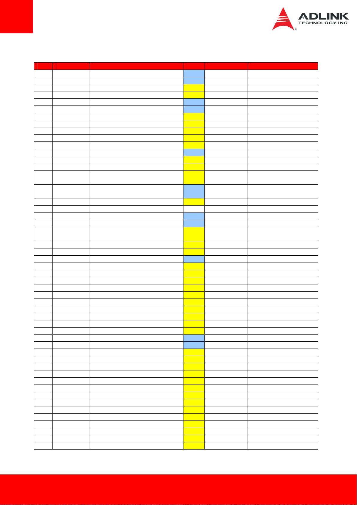
5 Pinouts and Signal Descriptions
Crossed out signals are not supported.
3V (3.3 V ±5%) is generated on board. Pins may be used to power devices on the carrier board
up to a maximum load of 500 mA.
Do not connect the 3V pin to external 3.3V supply power.
5.1 X1: PCI Bus, USB, Audio
Pin Signal Pin Signal Pin Signal Pin Signal
1 GND 2 GND 51 VCC 52 VCC
3 PCICLK3 4 PCICLK4 53 PAR 54 SERR#
5 GND 6 GND 55 GPERR# 56 RESERVED
7 PCICLK1 8 PCICLK2 57 PME# 58 USB29 REQ3# 10 GNT3# 59 LOCK# 60 DEVSEL#
11 GNT2# 12 3V 61 TRDY# 62 USB313 REQ2# 14 GNT1# 63 IRDY# 64 STOP#
15 REQ1# 16 3V 65 FRAME# 66 USB2+
17 GNT0# 18 RESERVED 67 GND 68 GND
19 VCC 20 VCC 69 AD16 70 CBE2#
21 SERIRQ 22 REQ0# 71 AD17 72 USB3+
23 AD0 24 3V 73 AD19 74 AD18
25 AD1 26 AD2 75 AD20 76 USB027 AD4 28 AD3 77 AD22 78 AD21
29 AD6 30 AD5 79 AD23 80 USB131 CBE0# 32 AD7 81 AD24 82 CBE3#
33 AD8 34 AD9 83 VCC 84 VCC
35 GND 36 GND 85 AD25 86 AD26
37 AD10 38 AUXAL 87 AD28 88 USB0+
39 AD11 40 MIC 89 AD27 90 AD29
41 AD12 42 AUXAR 91 AD30 92 USB1
43 AD13 44 ASVCC 93 PCIRST# 94 AD31
45 AD14 46 SNDL 95 INTC# 96 INTD#
47 AD15 48 ASGND 97 INTA# 98 INTB#
49 CBE1# 50 SNDR
99 GND 100 GND
Page 15
Page 16
X1 Signal Descriptions
Pin Signal Description Type PU/PD Comment
1 GND Ground PWR - 2 GND Ground PWR - 3 PCICLK3 PCI Clock Slot 3 O-3,3 - 4 PCICLK4 PCI Clock Slot 4 O-3,3 - 5 GND Ground PWR - 6 GND Ground PWR - 7 PCICLK1 PCI Clock Slot 1 O-3,3 - 8 PCICLK2 PCI Clock Slot 2 O-3,3 - -
9 REQ3# PCI Bus Request 3 I-3,3 PU 8k2 3,3V 10 GNT3# PCI Bus Grant 3 O-3,3 - 11 GNT2# PCI Bus Grant 2 O-3,3 - 12 3V Power +3,3V PWR - 13 REQ2# PCI Bus Request 2 I-3,3 PU 8k2 3,3V 14 GNT1# PCI Bus Grant 1 O-3,3 - -
15 REQ1# PCI Bus Request 1 I-3,3 PU 4K to 3V3
16 3V Power +3,3V PWR PU 8.2K to 3.3V
17 GNT0# PCI Bus Grant 0 O-3,3 - 18 RESERVED NC -
19 5VCC Power +5V PWR - 20 5VCC Power +5V PWR - -
21 SERIRQ Serial Interrupt Reqest
22 REQ0# PCI Bus Request 0 I-3,3 PU 8k2 3,3V 23 AD0 PCI Address & Data Bus line IO-3,3 -
24 3V Power +3,3V PWR - 25 AD1 PCI Address & Data Bus line IO-3,3 - 26 AD2 PCI Address & Data Bus line IO-3,3 - 27 AD4 PCI Address & Data Bus line IO-3,3 - 28 AD3 PCI Address & Data Bus line IO-3,3 - 29 AD6 PCI Address & Data Bus line IO-3,3 - 30 AD5 PCI Address & Data Bus line IO-3,3 - 31 CBE0# PCI Bus Command and Byte enables 0 IO-3,3 - 32 AD7 PCI Address & Data Bus line IO-3,3 - 33 AD8 PCI Address & Data Bus line IO-3,3 - 34 AD9 PCI Address & Data Bus line IO-3,3 - 35 GND Ground PWR - 36 GND Ground PWR - 37 AD10 PCI Address & Data Bus line IO-3,3 - 38 AUXAL Auxiliary Line Input Left I
39 AD11 PCI Address & Data Bus line IO-3,3 - 40 MIC Microphone Input I - 41 AD12 PCI Address & Data Bus line IO-3,3 - 42 AUXAR Auxiliary Line Input Right I
43 AD13 PCI Address & Data Bus line IO-3,3 - 44 ASVCC Analog Supply of Sound Controller O-5 - 45 AD14 PCI Address & Data Bus line IO-3,3 - 46 SNDL Audio Out Left O - 47 AD15 PCI Address & Data Bus line IO-3,3 - 48 ASGND Analog Ground of Sound Controller P - 49 CBE1# PCI Bus Command and Byte enables 1 IO-3,3 - 50 SNDR Audio Out Right O - -
IO-
3,3
PU 8k2 3,3V -
Before level shifter, only
measurable when energized
Only measurable when
switch is energized
Page 16
Page 17
Pin Signal Description Type PU/PD Comment
51 5VCC Power +5V PWR
52 5VCC Power +5V PWR
53 PAR PCI Bus Parity IO-3,3
54 SERR# PCI Bus System Error IO-3,3 PU 8k2 3,3V
55 GPERR# PCI Bus Grant Error IO-3,3 PU 8k2 3,3V
56 RESERVED NC -
57 PME# PCI Power Management Event IO-3,3 PU 10k 3,3VSB 58 USB2N USB Data- Port2 I/O - DP
59 LOCK# PCI Bus Lock IO-3,3 PU 8k2 3,3V
60 DEVSEL# PCI Bus Device Select IO-3,3 PU 8k2 3,3V
61 TRDY# PIC Bus Target Ready IO-3,3 PU 8k2 3,3V
62 USB3N USB Data- Port3 I/O - DP
63 IRDY# PCI Bus Initiator Ready IO-3,3 PU 8k2 3,3V
64 STOP# PCI Bus Stop IO-3,3 PU 8k2 3,3V
65 FRAME# PCI Bus Cycle Frame IO-3,3 PU 8k2 3,3V
66 USB2P USB Data+ Port2 I/O - DP
67 GND Ground PWR
68 GND Ground PWR
69 AD16 PCI Address & Data Bus line IO-3,3
70 CBE2# PCI Bus Command and Byte enables 2 IO-3,3
71 AD17 PCI Address & Data Bus line IO-3,3
72 USB3P USB Data+ Port3 I/O - DP
73 AD19 PCI Address & Data Bus line IO-3,3
74 AD18 PCI Address & Data Bus line IO-3,3
75 AD20 PCI Address & Data Bus line IO-3,3
76 USB0N USB Data- Port0 I/O - DP
77 AD22 PCI Address & Data Bus line IO-3,3
78 AD21 PCI Address & Data Bus line IO-3,3
79 AD23 PCI Address & Data Bus line IO-3,3
80 USB1N USB Data- Port1 I/O - DP
81 AD24 PCI Address & Data Bus line IO-3,3
82 CBE3# PCI Bus Command and Byte enables 3 IO-3,3
83 5VCC Power +5V PWR
84 5VCC Power +5V PWR
85 AD25 PCI Address & Data Bus line IO-3,3
86 AD26 PCI Address & Data Bus line IO-3,3
87 AD28 PCI Address & Data Bus line IO-3,3
88 USB0P USB Data+ Port0 I/O - DP
89 AD27 PCI Address & Data Bus line IO-3,3
90 AD29 PCI Address & Data Bus line IO-3,3
91 AD30 PCI Address & Data Bus line IO-3,3
92 USB1P USB Data+ Port1 I/O - DP
93 PCIRST# PCI Bus Reset O-3,3
94 AD31 PCI Address & Data Bus line IO-3,3
95 INTC# PCI BUS Interrupt Reauest C I-3,3 PU 8k2 3,3V
96 INTD# PCI BUS Interrupt Reauest D I-3,3 PU 8k2 3,3V
97 INTA# PCI BUS Interrupt Reauest A I-3,3 PU 8k2 3,3V
98 INTB# PCI BUS Interrupt Reauest B I-3,3 PU 8k2 3,3V
99 GND Ground PWR
100 GND Ground PWR
Page 17
Page 18
5.2 X2: ISA
Pin Signal Pin Signal Pin Signal Pin Signal
1 GND 2 GND 51 VCC 52 VCC
3 SD14 4 SD15 53 SA6 54 IRQ5
5 SD13 6 MASTER# 55 SA7 56 IRQ6
7 SD12 8 DREQ7 57 SA8 58 IRQ7
9 SD11 10 DACK7# 59 SA9 60 SYSCLK
11 SD10 12 DREQ6 61 SA10 62 REFSH#
13 SD9 14 DACK6# 63 SA11 64 DREQ1
15 SD8 16 DREQ5 65 SA12 66 DACK1#
17 MEMW# 18 DACK5# 67 GND 68 GND
19 MEMR# 20 DREQ0 69 SA13 70 DREQ3
21 LA17 22 DACK0# 71 SA14 72 DACK3#
23 LA18 24 IRQ14 73 SA15 74 IOR#
25 LA19 26 IRQ15 75 SA16 76 IOW#
27 LA20 28 IRQ12 77 SA18 78 SA17
29 LA21 30 IRQ11 79 SA19 80 SMEMR#
31 LA22 32 IRQ10 81 IOCHRDY 82 AEN
33 LA23 34 IO16# 83 VCC 84 VCC
35 GND 36 GND 85 SD0 86 SMEMW#
37 SBHE# 38 M16# 87 SD2 88 SD1
39 SA0 40 OSC 89 SD3 90 NOWS#
41 SA1 42 BALE 91 DREQ2 92 SD4
43 SA2 44 TC 93 SD5 94 IRQ9
45 SA3 46 DACK2# 95 SD6 96 SD7
47 SA4 48 IRQ3 97 IOCHK# 98 RSTDRV
49 SA5 50 IRQ4
99 GND 100 GND
Page 18
Page 19
X2 Signal Descriptions
Pin Signal Description Type PU/PD Comment
1 GND Ground PWR - -
2 GND Ground PWR - -
3 SD14 ISA Data Bus IO-5 PU 4k7 5V int. PU 100k 5V in
4 SD15 ISA Data Bus IO-5 PU 4k7 5V int. PU 100k 5V in
5 SD13 ISA Data Bus IO-5 PU 4k7 5V int. PU 100k 5V in
6 MASTER# ISA 16-Bit Master I-5 PU 8K2 5V -
7 SD12 ISA Data Bus IO-5 PU 4k7 5V int. PU 100k 5V in
8 DREQ7 ISA DMA Request 7 I-5 PD 4k7 to GND -
9 SD11 ISA Data Bus IO-5 PU 4k7 5V int. PU 100k 5V in
10 DACK7# ISA DMA Acknowledge 7 IO-5 no PU/PD int. PU 100k 5V in
11 SD10 ISA Data Bus IO-5 PU 4k7 5V int. PU 100k 5V in
12 DREQ6 ISA DMA Request 6 I-5 PD 4k7 to GND 13 SD9 ISA Data Bus IO-5 PU 4k7 5V int. PU 100k 5V in
14 DACK6# ISA DMA Acknowledge 6 IO-5 no PU/PD int. PU 100k 5V in
15 SD8 ISA Data Bus IO-5 PU 4k7 5V int. PU 100k 5V in
16 DREQ5 ISA DMA Request 5 I-5 PD 4k7 to GND 17 MEMW# ISA Memory Write IO-5 PU 8k2 5V int. PU 100k 5V in
18 DACK5# ISA DMA Acknowledge 5 IO-5 no PU/PD int. PU 100k 5V in
19 MEMR# ISA Memory Read IO-5 PU 8k2 5V int. PU 100k 5V in
20 DREQ0 ISA DMA Request 0 I-5 PD 4k7 to GND 21 LA17 ISA Address Bus (SA17) O-5 PU 4k7 5V int. PU 100k 5V in
22 DACK0# ISA DMA Acknowledge 0 IO-5 no PU/PD 23 LA18 ISA Address Bus (SA18) O-5 PU 4k7 5V int. PU 100k 5V in
24 IRQ14
25 LA19 ISA Address Bus (SA19) O-5 PU 4k7 5V int. PU 100k 5V in
26 IRQ15 ISA Interrupt Request 15 IO-5 PU 4k7 5V 27 LA20 ISA Address Bus (SA20) O-5 PU 4k7 5V int. PU 100k 5V in
28 IRQ12 ISA Interrupt Request 12 IO-5 PU 4k7 5V 29 LA21 ISA Address Bus (SA21) O-5 PU 4k7 5V int. PU 100k 5V in
30 IRQ11 ISA Interrupt Request 11 IO-5 PU 4k7 5V 31 LA22 ISA Address Bus (SA22) O-5 PU 4k7 5V int. PU 100k 5V in
32 IRQ10 ISA Interrupt Request 10 IO-5 PU 4k7 5V 33 LA23 ISA Address Bus (SA23) O-5 PU 4k7 5V int. PU 100k 5V in
34 IO16# ISA 16-Bit I/O Access I-5 PU 1K 5V 35 GND Ground PWR - 36 GND Ground PWR - 37 SBHE# ISA System Byte High Enable IO-5 PU 4k7 5V int. PU 100k 5V in
38 M16# ISA 16-Bit Memory Access IO-5 PU 1K 5V 39 SA0 ISA Address Bus O-5 PU 4k7 5V int. PU 100k 5V in
40 OSC ISA Oscillator (CLK_ISA14#) O-3,3 - 41 SA1 ISA Address Bus O-5 PU 4k7 5V int. PU 100k 5V in
42 BALE ISA Buffer Address Latch Enable IO-5 PD 4k7 int. PU 100k 5V in
43 SA2 ISA Address Bus O-5 PU 4k7 5V int. PU 100k 5V in
44 TC ISA Terminal Count IO-5 PD 4k7 45 SA3 ISA Address Bus O-5 PU 4k7 5V int. PU 100k 5V in
46 DACK2# ISA DMA Acknowledge 2 IO-5 no PU/PD 47 SA4 ISA Address Bus O-5 PU 4k7 5V int. PU 100k 5V in
48 IRQ3 ISA Interrupt Request 3 IO-5 PU 4k7 5V 49 SA5 ISA Address Bus O-5 PU 4k7 5V int. PU 100k 5V in
50 IRQ4 ISA Interrupt Request 4 IO-5 PU 4k7 5V -
ISA Interrupt Request 14 / ROMChip
Select
IO-5 PU 4k7 5V -
Page 19
Page 20
Pin Signal Description Type PU/PD Comment
51 5VCC Power +5V PWR - 52 5VCC Power +5V PWR - 53 SA6 ISA Address Bus O-5 PU 4k7 5V int. PU 100k 5V in
54 IRQ5 ISA Interrupt Request 5 IO-5 PU 4k7 5V 55 SA7 ISA Address Bus O-5 PU 4k7 5V int. PU 100k 5V in
56 IRQ6 ISA Interrupt Request 6 IO-5 PU 4k7 5V 57 SA8 ISA Address Bus O-5 PU 4k7 5V int. PU 100k 5V in
58 IRQ7 ISA Interrupt Request 7 IO-5 PU 4k7 5V 59 SA9 ISA Address Bus O-5 PU 4k7 5V int. PU 100k 5V in
60 SYSCLK ISA Bus Clock (CLK_SYS_ISA) O-3,3 - 61 SA10 ISA Address Bus O-5 PU 4k7 5V int. PU 100k 5V in
62 REFSH# ISA System Refresh Control IO-5 PU 1k 5V int. PU 100k 5V in
63 SA11 ISA Address Bus O-5 PU 4k7 5V int. PU 100k 5V in
64 DREQ1 ISA DMA Request 1 I-5 PD 4k7 to GND 65 SA12 ISA Address Bus O-5 PU 4k7 5V int. PU 100k 5V in
66 DACK1# ISA DMA Acknowledge 1 IO-5 no PU/PD 67 GND Ground PWR - 68 GND Ground PWR - 69 SA13 ISA Address Bus O-5 PU 4k7 5V int. PU 100k 5V in
70 DREQ3 ISA DMA Request 3 I-5 PD 4k7 to GND 71 SA14 ISA Address Bus O-5 PU 4k7 5V int. PU 100k 5V in
72 DACK3# ISA DMA Acknowledge 3 IO-5 no PU/PD 73 SA15 ISA Address Bus O-5 PU 4k7 5V int. PU 100k 5V in
74 IOR# ISA I/O Read IO-5 PU 8k2 5V int. PU 100k 5V in
75 SA16 ISA Address Bus O-5 PU 4k7 5V int. PU 100k 5V in
76 IOW# ISA I/O Write IO-5 PU 8k2 5V int. PU 100k 5V in
77 SA18 ISA Address Bus O-5 PU 4k7 5V int. PU 100k 5V in
78 SA17 ISA Address Bus O-5 PU 4k7 5V int. PU 100k 5V in
79 SA19 ISA Address Bus O-5 PU 4k7 5V int. PU 100k 5V in
80 SMEMR# ISA System Memory Read IO-5 PU 1k 5V 81 IOCHRDY ISA I/O Channel Ready IO-5 PU 1k 5V 82 AEN ISA Address Enable IO-5 PD 4k7 83 5VCC Power +5V PWR - 84 5VCC Power +5V PWR - 85 SD0 ISA Data Bus IO-5 PU 4k7 5V int. PU 100k 5V in
86 SMEMW# ISA System Memory Write IO-5 PU 1k 5V 87 SD2 ISA Data Bus IO-5 PU 4k7 5V int. PU 100k 5V in
88 SD1 ISA Data Bus IO-5 PU 4k7 5V int. PU 100k 5V in
89 SD3 ISA Data Bus IO-5 PU 4k7 5V int. PU 100k 5V in
90 NOWS# ISA No Wait Staits I-5 PU1K 5V 91 DREQ2 ISA DMA Request 2 I-5 PD 4k7 to GND 92 SD4 ISA Data Bus IO-5 PU 4k7 5V int. PU 100k 5V in
93 SD5 ISA Data Bus IO-5 PU 4k7 5V int. PU 100k 5V in
94 IRQ9 ISA Interrupt Request 9 IO-5 PU 4k7 5V 95 SD6 ISA Data Bus IO-5 PU 4k7 5V int. PU 100k 5V in
96 SD7 ISA Data Bus IO-5 PU 4k7 5V int. PU 100k 5V in
97 IOCHK# ISA I/O Channel Check I-5 PU 4k7 5V 98 RSTDRV ISA Reset O-5 - 99 GND Ground PWR - -
100 GND Ground PWR - -
Page 20
Page 21
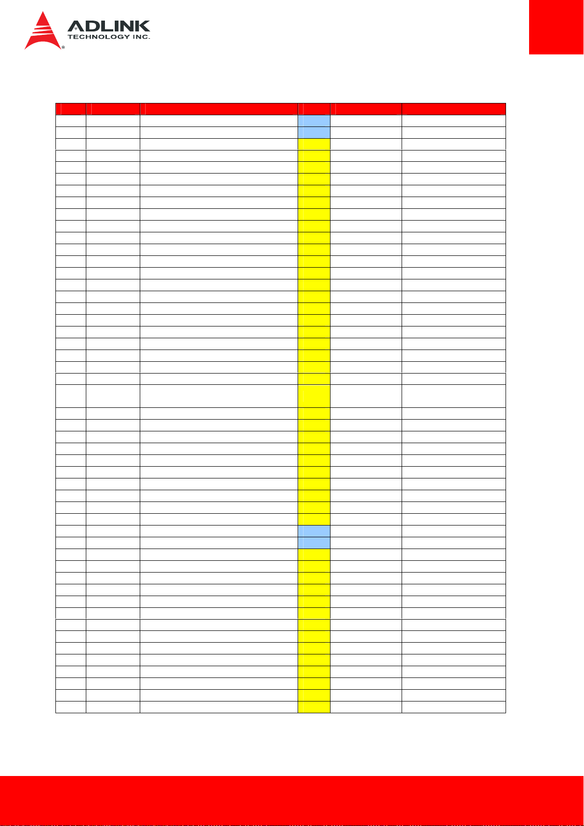
5.3 X3: LVDS, Serial, Parallel, KB, MS
Pin Signal Pin Signal Pin Signal Pin Signal
1 GND 2 GND 51 LPT/FLPY# 52 RESERVED
3 R 4 B 53 VCC 54 GND
5 HSY 6 G 55 STB# 56 AFD#
7 VSY 8 DDCK 57 RESERVED 58 PD7
9 DETECT# 10 DDDA 59 IRRX 60 ERR#
11 LCDDO16 12 LCDDO18 61 IRTX 62 PD6
13 LCDDO17 14 LCDDO19 63 RXD2 64 INIT#
15 GND 16 GND 65 GND 66 GND
17 LCDDO13 18 LCDDO15 67 RTS2# 68 PD5
19 LCDDO12 20 LCDDO14 69 DTR2# 70 SLIN#
21 GND 22 GND 71 DCD2# 72 PD4
23 LCDDO8 24 LCDDO11 73 DSR2# 74 PD3
25 LCDDO9 26 LCDDO10 75 CTS2# 76 PD2
27 GND 28 GND 77 TXD2 78 PD1
29 LCDDO4 30 LCDDO7 79 RI2# 80 PD0
31 LCDDO5 32 LCDDO6 81 VCC 82 VCC
33 GND 34 GND 83 RXD1 84 ACK#
35 LCDDO1 36 LCDDO3 85 RTS1# 86 BUSY
37 LCDDO0 38 LCDDO2 87 DTR1# 88 PE
39 VCC 40 VCC 89 DCD1# 90 SLCT#
41 JILI_DAT 42 LTGIO0 91 DSR1# 92 MSCLK
43 JILI_CLK 44 BLON# 93 CTS1# 94 MSDAT
45 BIASON 46 DIGON 95 TXD1 96 KBCLK
47 COMP 48 Y 97 RI1# 98 KBDAT
49 SYNC 50 C
99 GND 100 GND
Page 21
Page 22

X3 Signal Descriptions
Pin Signal Description Type PU/PD Comment
1 GND Ground PWR - 2 GND Ground PWR - 3 R Analog Video Out RGB - Red Ch OA PD 150R 4 B Analog Video Out RGB - Blue Ch OA PD 150R 5 HSY Horizontal Synchronization Pulse O-3,3 - 6 G Analog Video Out RGB - Green Ch OA PD 150R 7 VSY Vertical Synchronization Pulse O-3,3 - -
8 DDCK Display Data Channel Clock IO-5 PU 2.2K to 5V
9 DETECT# Panel Hot-Plug Detection NC 10 DDDA Display Data Channel Data IO-5 PU 2.2K to 5V
11 LCD16 Second LVDS Ch Data Txclk - O - DP - -
12 LCD18 Second LVDS Ch Data Txout 3- O - DP - 13 LCD17 Second LVDS Ch Data Txclk + O - DP - 14 LCD19 Second LVDS Ch Data Txout 3+ O - DP - 15 GND Ground PWR - 16 GND Ground PWR - 17 LCD13 Second LVDS Ch Data Txout 1+ O - DP - 18 LCD15 Second LVDS Ch Data Txout 2+ O - DP - 19 LCD12 Second LVDS Ch Data Txout 1- O - DP - 20 LCD14 Second LVDS Ch Data Txout 2- O - DP - 21 GND Ground PWR - 22 GND Ground PWR - 23 LCD8 First LVDS Ch Data Txout 3- O - DP - 24 LCD11 Second LVDS Ch Data Txout 0+ O - DP - 25 LCD9 First LVDS Ch Data Txout 3+ O - DP - 26 LCD10 Second LVDS Ch Data Txout 0- O - DP - 27 GND Ground PWR - 28 GND Ground PWR - 29 LCD4 First LVDS Ch Data Txout 2- O - DP - 30 LCD7 First LVDS Ch Data Txclk + O - DP - 31 LCD5 First LVDS Ch Data Txout 2+ O - DP - 32 LCD6 First LVDS Ch Data Txclk - O - DP - 33 GND Ground PWR - 34 GND Ground PWR - 35 LCD1 First LVDS Ch Data Txout 0+ O - DP - 36 LCD3 First LVDS Ch Data Txout 1+ O - DP - 37 LCD0 First LVDS Ch Data Txout 0- O - DP - 38 LCD2 First LVDS Ch Data Txout 1- O - DP - 39 5VCC Power +5V PWR - 40 5VCC Power +5V PWR - 41 JILI_DAT JILI I2C Data Signal IO-3,3 PU 2.2k 3,3V 42 LTGIO0 Display Backlight Control O-5 - 43 JILI_CLK JILI I2C Clock Signal IO-3,3 PU 2.2k 3,3V 44 BLON# Display Backlight On O-3.3 - 45 BIASON Display Contrast O-5 - 46 DIGON Display Power On O-3.3 - 47 COMP Composite Video / SCART Blue NC - 48 Y S-Video Luminance / SCART Red NC - 49 SYNC Composite Sync NC - -
50 C
S-Video Chrominance / SCART
Green
NC - -
Behind diode that may
influence meas.
Behind diode that may
influence meas.
Page 22
Page 23

Pin Signal Description Type PU/PD Comment
51 LPT | FLPY# LPT / Floppy Interface Select NC - 52 RESERVED NC -
53 5VCC Power +5V PWR - 54 GND Ground PWR - 55 STB# | RSV LPT Strobe Signal O-5 - 56 AFD# | DENSEL LPT Automatic Feed / Floppy Density Select O-5 - 57 RESERVED NC -
58 PD7 | RSV LPT Data Bus D7 IO-5 - 59 IRRX Infrared Receive I-5 - 60 ERR# | HDSEL# LPT Error / Floppy Head Select IO-5 - 61 IRTX Infrared Transmit O-5 - 62 PD6 | RSV LPT Data Bus D6 IO-5 - 63 RXD2 Data Receive COM2 I-5 - 64 INIT# | DIR# LPT Initiate / Floppy Direction O-5 - 65 GND Ground PWR - 66 GND Ground PWR - 67 RTS2# Request to Send COM2 O-5 - 68 PD5 | RSV LPT Data Bus D5 IO-5 - 69 DTR2# Data Terminal Ready COM2 O-5 - 70 SLIN# | STEP# LPT Select / Floppy Motor Step O-5 - 71 DCD2# Data Carrier Detect COM2 I-5 - 72 PD4 | DSKCHG# LPT Data Bus D4 IO-5 - 73 DSR2# Data Set Ready COM2 I-5 - 74 PD3 | RDATA# LPT Data Bus D3 IO-5 - 75 CTS2# Clear to Send COM2 I-5 - 76 PD2 | WP# LPT Data Bus D2 IO-5 - 77 TXD2 Data Transmit COM2 O-3.3 PU 1k 3.3V 78 PD1 | TRK0# LPT Data Bus D1 IO-5 - 79 RI2# Ring Indicator COM2 I-5 - 80 PD0 | INDEX# LPT Data Bus D0 IO-5 - 81 5VCC Power +5V PWR - 82 5VCC Power +5V PWR - 83 RXD1# Data Receive COM1 I-5 - 84 ACK# | DRV LPT Acknowledge / Floppy Drive Select IO-5 - 85 RTS1# Request to Send COM1 O-5 PD 1k 86 BUSY# | MOT LPT Busy / Floppy Motor Select IO-5 - 87 DTR1# Data Terminal Ready COM1 O-5 - 88 PE | WDATA# LPT Paper Empty / Floppy Raw Write Data IO-5 - 89 DCD1# Data Carrier Detect COM1 I-5 - 90 SLCT#|WGATE# LPT Power On / Floppy Write Enable IO-5 - 91 DSR1# Data Set Ready COM1 I-5 - 92 MSCLK Mouse Clock O-5 PU 4k7 5V 93 CTS1# Clear to Send COM1 I-5 - 94 MSDAT Mouse Data IO-5 PU 4k7 5V 95 TXD1 Data Transmit COM1 O-5 PU 1k 3.3V 96 KBCLK Keyboard Clock O-5 PU 4k7 5V 97 RI1# Ring Indicator COM1 I-5 - 98 KBDAT Keyboard Data IO-5 PU 4k7 5V 99 GND Ground PWR - -
100 GND Ground PWR - -
Page 23
Page 24

5.4 X4: IDE 1, IDE 2, Ethernet, Miscellaneous
Pin Signal Pin Signal Pin Signal Pin Signal
1 GND 2 GND 51 SIDE_IOW# 52 PIDE_IOR#
3 5V_SB 4 PWGIN 53 SIDE_DRQ 54 PIDE_IOW#
5 PS_ON# 6 SPEAKER 55 SIDE_D15 56 PIDE_DRQ
7 PWRBTN# 8 BATT 57 SIDE_D0 58 PIDE_D15
9 KBINH# 10 LILED# 59 SIDE_D14 60 PIDE_D0
11 RSMRST# 12 ACTLED# 61 SIDE_D1 62 PIDE_D14
13 ROMKBCS# 14 SPEEDLED# 63 SIDE_D13 64 PIDE_D1
15 EXT_PRG 16 I2CLK 65 GND 66 GND
17 VCC 18 VCC 67 SIDE_D2 68 PIDE_D13
19 OVCR# 20 GPCS# 69 SIDE_D12 70 PIDE_D2
21 EXTSMI# 22 I2DAT 71 SIDE_D3 72 PIDE_D12
23 SMBCLK 24 SMBDATA 73 SIDE_D11 74 PIDE_D3
25 SIDE_CS3# 26 SMBALRT# 75 SIDE_D4 76 PIDE_D11
27 SIDE_CS1# 28 DASP_S 77 SIDE_D10 78 PIDE_D4
29 SIDE_A2 30 PIDE_CS3# 79 SIDE_D5 80 PIDE_D10
31 SIDE_A0 32 PIDE_CS1# 81 VCC 82 VCC
33 GND 34 GND 83 SIDE_D9 84 PIDE_D5
35 PDIAG_S 36 PIDE_A2 85 SIDE_D6 86 PIDE_D9
37 SIDE_A1 38 PIDE_A0 87 SIDE_D8 88 PIDE_D6
39 SIDE_INTRQ 40 PIDE_A1 89 GPE2# 90 CBLID_P
41 BATLOW# 42 GPE1# 91 RXD- 92 PIDE_D8
43 SIDE_AK# 44 PIDE_INTRQ 93 RXD+ 94 SIDE_D7
45 SIDE_RDY 46 PIDE_AK# 95 TXD- 96 PIDE_D7
47 SIDE_IOR# 48 PIDE_RDY 97 TXD+ 98 HDRST#
49 VCC 50 VCC
99 GND 100 GND
Page 24
Page 25

X4 Signal Descriptions
Pin Signal Description Type PU/PD Comment
1 GND Ground PWR - 2 GND Ground PWR - 3 5V_SB Supply of internal suspend Circuit PWR - 4 PWGIN Power Good / Reset Input I-3,3 - 5 PS_ON Power Supply On O-5 PU 4k7 5VSB 6 SPEAKER Speaker Output O-5 - 7 PWRBTN# Power Button I-5 PU 10k 3,3BMC 8 BATT Battery Supply PWR - -
9 KBINH Keyboard Inhibit Control Input NC - 10 LILED Ethernet Link LED O-3,3 - 11 RSMRST# Resume Reset input I-3,3 PU 10k 3,3VSB 12 ACTLED Ethernet Activity LED O-3,3 - 13 ROMKBCS# - NC - 14 SPDLED Ethernet Speed LED O-3,3 - 15 EXT_PRG - NC - 16 I2CLK I2C Bus Clock O-5 PU 2.2k 5V
17 5VCC Power +5V PWR - 18 5VCC Power +5V PWR - 19 OVCR# Over Current Detect for USB I-3,3 PU 10k 3,3VSB 20 GPCS# - NC - 21 EXTSMI# System Management Interrupt Input I-3,3 PU 10k 3,3V To be verified
22 I2DAT I2C Bus Data IO-5 PU 2.2k 5V 23 SMBCLK SM Bus Clock O-3,3 PU 2k2 3,3VSB 24 SMBDATA SM Bus Data IO-3,3 PU 2k2 3,3VSB 25 S_CS3# Secondary IDE Chip Select Channel 1 O-3,3 - 26 SMBALERT SM Bus Alert I-3,3 PU 10k 3,3VSB 27 S_CS1# Secondary IDE Chip Select Channel 0 O-3,3 - 28 DASP_S - I-3,3 - 29 S_A2 Secondary IDE Address Bus O-3,3 - 30 P_CS3# Primary IDE Chip Select Channel 1 O-3,3 - 31 S_A0 Secondary IDE Address Bus O-3,3 - 32 P_CS1# Primary IDE Chip Select Channel 0 O-3,3 - 33 GND Ground PWR - 34 GND Ground PWR - 35 PDIAG_S 80-conductor IDE cable Channel 1 I-3,3 - 36 P_A2 Primary IDE Address Bus O-3,3 - 37 S_A1 Secondary IDE Address Bus O-3,3 - 38 P_A0 Primary IDE Address Bus O-3,3 - 39 S_INTRQ Secondary IDE Interrupt Request I-3,3 PD 10k 40 P_A1 Primary IDE Address Bus O-3,3 - 41 BATLOW# Battery Low I-3,3 42 GPE1# - NC - 43 S_AK# Secondary IDE DMA Acknowledge O-3,3 - 44 P_INTRQ Primary IDE Interrupt Request I-3,3 PD 10k 45 S_RDY Secondary IDE Ready I-3,3 PU 5k6 3,3V 46 P_AK# Primary IDE DMA Acknowledge O-3,3 - 47 S_IOR# Secondary IDE IO Read O-3,3 - 48 P_RDY Primary IDE Ready I-3,3 PU 5k6 3,3V 49 5VCC Power +5V PWR - 50 5VCC Power +5V PWR - -
Page 25
Page 26

Pin Signal Description Type PU/PD Comment
51 S_IOW# Secondary IDE IO Write O-3,3 - 52 P_IOR# Primary IDE IO Read O-3,3 - 53 S_DRQ Secondary IDE DMA Request I-3,3 PD 5k6 54 P_IOW# Primary IDE IO Write O-3,3 - 55 S_D15 Secondary IDE Data Bus IO - 56 P_DRQ Primary IDE DMA Request I-3,3 PD 5k6 57 S_D0 Secondary IDE Data Bus IO - 58 P_D15 Primary IDE Data Bus IO - 59 S_D14 Secondary IDE Data Bus IO - 60 P_D0 Primary IDE Data Bus IO - 61 S_D1 Secondary IDE Data Bus IO - 62 P_D14 Primary IDE Data Bus IO - 63 S_D13 Secondary IDE Data Bus IO - 64 P_D1 Primary IDE Data Bus IO - 65 GND Ground PWR - 66 GND Ground PWR - 67 S_D2 Secondary IDE Data Bus IO - 68 P_D13 Primary IDE Data Bus IO - 69 S_D12 Secondary IDE Data Bus IO - 70 P_D2 Primary IDE Data Bus IO - 71 S_D3 Secondary IDE Data Bus IO - 72 P_D12 Primary IDE Data Bus IO - 73 S_D11 Secondary IDE Data Bus IO - 74 P_D3 Primary IDE Data Bus IO - 75 S_D4 Secondary IDE Data Bus IO - 76 P_D11 Primary IDE Data Bus IO - 77 S_D10 Secondary IDE Data Bus IO - 78 P_D4 Primary IDE Data Bus IO - 79 S_D5 Secondary IDE Data Bus IO - 80 P_D10 Primary IDE Data Bus IO - 81 5VCC Power +5V PWR - 82 5VCC Power +5V PWR - 83 S_D9 Secondary IDE Data Bus IO - 84 P_D5 Primary IDE Data Bus IO - 85 S_D6 Secondary IDE Data Bus IO - 86 P_D9 Primary IDE Data Bus IO - 87 S_D8 Secondary IDE Data Bus IO - 88 P_D6 Primary IDE Data Bus IO - 89 GPE2# - NC - 90 CBLID_P# 80-conductor IDE cable Channel 0 I-3,3 - 91 RXD# Ethernet Receive Differential Signal ( RXD-) I - DP - 92 P_D8 Primary IDE Data Bus IO - 93 RXD Ethernet Receive Differential Signal ( RXD+) I - DP - 94 S_D7 Secondary IDE Data Bus IO PD 10k 95 TXD# Ethernet Transmit Differential Signal (TXD-) O -DP - 96 P_D7 Primary IDE Data Bus IO PD 10k 97 TXD Ethernet Transmit Differential Signal (TXD+) O -DP - 98 HDRST# Hard Drive Reset O-3,3 - 99 GND Ground PWR - -
100 GND Ground PWR - -
Page 26
Page 27

6 Module Interfaces
This chapter describes connectors with pin outs, LEDs and switches that are used on the module
but which interfaces are not part of the ETX standard specification
6.1 Connector, Switch and LED Locations
Component Side
GbE
Fan
Reset BIOS
CMOS
SW2
System
LEDs
DisplayPort
DB40
Debug
XDP port
PCI IRQ
Selection
SW4
Page 27
Page 28

Solder Side
PCI Voltage
Selection
SW3
SPI Boot
Selection
SW1
Page 28
Page 29

6.2 40-pin Multipurpose Connector
FPC Connector Type: FCI 59GF Flex 10042867
Pin Orientation:
1 40
Pin Definitions (on ETX module)
Pin Interface Signal Remark Pin Interface Signal Remark
40 VCC_SPI_IN SPI Power Input from
SPI
Program
interface
39 GND 19 RXD6
38 SPI_BIOS_CS0# 18 FUMD0
37 SPI_BIOS_CS1# 17 RESET_IN#
36 SPI_BIOS_MISO 16 DATA
35 SPI_BIOS_MOSI 15 CLK
34
33 3V3_LPC System power 3.3V
LPC Bus
32 GND 12 PWRBTN#
31 BIOS_DIS0 11 SYS_RESET#
30 RST# 10 CB_RESET#
29 CLK33_LPC 9 CB_PWROK
28 LPC_FRAME# 8 SUS_S3#
27 LPC_AD3 7 SUS_S4#
26 LPC_AD2 6
25 LPC_AD1 always power 3.3V
24
23
BMC
Program
interface
22 3.3V_BMC always power 3.3V
21
SPI_BIOS_CLK 14 OCD0A Include a jumper to
LPC_AD0 4 SEL_BIOS Connect to Jumper
3.3V_BMC always power 3.3V
GND 1 Reserved
flash tool to module.
HW need add MOS
FET to switch SPI
power for SPI ROM
provide from COM
module
provide from COM
module
provide from COM
module
provide from COM
module
20 TXD6
13
5 POSTWDT_DIS# Connect to Jumper
3 BIOS_MODE Connect to Jumper
2
BMC Program
interface
(continued)
Test points
BMC Debug
signals
connect OCD0A via
1K0 pull-up to
3.3V_BMC
OCD0B Include a jumper to
connect OCD0A via
1K0 pull-up to
3.3V_BMC
SUS_S5#
for Debug
for Debug
for Debug
BMC_STATUS
Note: the pin description on the DB40 Debug Module is the inverse of that on the ETX module.
Page 29
Page 30

ETX-BT and the DB40 Module connected
6.3 Status LEDs
To facilitate easier maintenance, status LED’s are mounted on the board.
LED1 LED2 LED3
LED Descriptions:
Name Color Connection Function
LED1 Blue BMC output Power Sequence Status Code (BMC)
Power Changes, RESET
(see Section 7.1 Exception Codes)
LED2 Green Power Source 3Vcc S0 LED ON
S3/S4/S5 LED OFF
ECO mode LED OFF
LED3 Red BMC output and
same signal as
WDT (B27) on BtB
connector
Page 30
Module power up LED OFF
Watchdog counting LED OFF
Watchdog timed out LED ON
Watchdog RESET LED ON
Rebooted after WD RESET LED ON
Rebooted after PWRBTN LED ON
Rebooted after RESET BTN LED OFF
Note: only a RESET not initiated by the BMC can clear the WD LED
(user action)
Page 31

6.4 XDP Debug Header
1 26
The debug port is a connection into a target-system environment that provides access to JTAG,
run control, system control, and observation resources. The XDP target system connector is a
Molex 26-pin 52435-2671 connector. Specific plating types, locking clips, and alignment pin
details of this connector can be obtained from Molex. No specific plating types, locking clips or
alignment pins are required for the XDP tool.
Pin Definitions (on ETX module)
Connector Type: Molex 26-pin 52435-2671
Pin XDP Signal Target Signal I/O Device Pin XDP Signal Target Signal I/O Devic
e
1 OBSFN_A0 TAP_PREQ# I/O SoC 2 OBSFN_A1 TAP_PRDY# I/O SoC
3 GND GND NA 4 OBSDATA_A[0] DBG[0] I/O SoC
5 OBSDATA_A[1] DBG[1] I/O SoC 6 GND GND NA
7 OBSDATA_A[2] DBG[2] I/O SoC 8 OBSDATA_A[3] DBG[3] I/O SoC
9 GND GND NA 10 HOOK0 PMC_RSMRST# I SoC
11 HOOK1 PMIC_PWRBTN# O System 12 HOOK2 PMC_CORE_PW
ROK
13 HOOK3 ILB_RTC_TEST# O SoC 14 HOOK4 Open NA
15 HOOK5 Open NA 16 VCCOBS_AB 1.8VS (SUS) I System
17 HOOK6 PMC_PLTRST# I SoC 18 HOOK7 PMC_RSTBTN# O SoC
19 GND GND NA 20 TDO TAP_TDO I SoC
21 TRSTn TAP_TRST# O SoC 22 TDI TAP_TDI O SoC
23 TMS TAP_TMS O SoC 24 TCK1 Open NA
25 GND GND NA 26 TCK0 TAP_TCK O SoC
I SoC
Refer to the "Bay Trail M/D/I Platform” Debug Port Design Guide (DPDG),
Document Number: 512816, Revision: 2.1
Testing on the XDP connector was carried out with Intel® System Studio 2014 – JTAG Debugger
ITP-XDP3
Page 31
Page 32

6.5 DP Connector
Connector Type: Wurth WE 6871 2214 522
1 22
The DP connector brings out DDI1 port of the Intel® Atom™ SoC as either DP or HDMI/DVI on a
flat cable connector.
Pin Definitions
Pin Signal Description (DP / HDMI) Pin Signal Description (DP / HDMI)
1 GND 11 DP_LANE3+ / TMDS1_CLK+
2 DP_LANE0+ / TMDS_DATA2+ 12 DP_LANE3- / TMDS1_CLK-
3 DP_LANE0- / TMDS_DATA2- 13 CONFIG1
4 GND 14 CONFIG2 (not used)
5 DP_LANE1+ / TMDS_DATA1+ 15 GND
6 DP_LANE1- / TMDS_DATA1- 16 DP_AUX+ / HMDI1_CTRLCLK (3.3V !)
7 GND 17 DP_AUX- / HMDI1_CTRDATA (3.3V !)
8 DP_LANE2+ / TMDS_DATA0+ 18 GND
9 DP_LANE2- / TMDS_DATA0- 19 DP_HPD# / HDMI_HPD# !!
10 GND 20 + DP_PWR only (3.3V)
11 DP_LANE3+ / TMDS1_CLK+ 21 + DP_PWR only (3.3V)
12 DP_LANE3- / TMDS1_CLK- 22 + DP_PWR only (3.3V)
6.5.1
Display Mode Selection
Display mode (DP or HDMI/DVI) can be selected by strapping pin 13 (CONFIG1).
Strapping should be done on the carrier as follows
6.5.2
Page 32
- Pull high to 3.3V (3VS0) for HDMI/DVI
- Pull to GND for DisplayPort mode
Power Output Modification for HDMI
For HDMI/DVI output, pins 16, 17, should be converted to 5V (5VS0) on the carrier by level
shifters
Page 33

For HDMI/DVI output, pins 20, 21, 22 should not be used but power should be sourced from 5V
(5VS0) rail on the carrier
6.6 Fan Connector
Connector Type: JVE 24W1125A-04M00
Pin Orientation:
1
2
3
4
Pin Definitions:
Pin Signal
1 FAN_PWMOUT
2 FAN_TACHIN
3 Ground
4 5V
Page 33
Page 34

6.7 GbE Connector
Normal support for 100/10 Mbps LAN is through the X4 connector. There is a build option to
disconnect these signals and instead route full 1000/100/10 Mbps support to the FPC connector
on the module.
Note: Standard modules will not include the FPC connector and
will only route LAN signals to the X4 connector.
Connector Type: FPC-CN-1*20P-RT-D5
Pin Definitions: Pin Orientation
Pin Signal
1 GND
2 LAN_MDI_N3_C
3 LAN_MDI_P3_C
4 GND
5 LAN_MDI_N2_C
6 LAN_MDI_P2_C
7 GND
8 LAN_MDI_N1_C
9 LAN_MDI_P1_C
10 GND
11 LAN_MDI_N0_C
12 LAN_MDI_P0_C
13 GND
14 GBE0_CTREF
15 LED2_1000-L
Page 34
16 LED2_100-L
17 LED1_LINK/ACT-L
18 NC
19 +V3P3A_LAN
20 +V3P3A_LAN
Page 35

6.8 SW1: SPI Boot Device Selection
The ETX-BT supports a form of fail-safe BIOS. In the case that the primary BIOS is corrupted and
the BIOS POST takes longer than normal, the system’s POST watchdog will time out and the
system will reset with the secondary SPI Flash BIOS assigned as primary.
For information on monitoring and operation of the fail-safe BIOS, please refer to SEMA
documentation.
The SW1 switch allows users to change the boot behavior of the module. It sets the module to
either fail safe-mode, or assigns SPI0 or SPI1 as the boot BIOS while providing access to the
other SPI flash device.
Switch Settings
SPI Function Pin 1 Pin 2 Comment
SPI0 fails-safe mode ON OFF Boot from SPI0, SPI1 is secondary SPI flash
SPI1 boot OFF OFF Boot from SPI1, no fail-safe, SPI0 not accessible
SPI0 boot ON ON Boot from SPI0, no fail-safe, SPI1 not accessible
SPI1 boot OFF ON Boot from SPI1, no fail-safe, SPI0 not accessible
6.9 SW2: BIOS Setup Defaults RESET Button
To perform a hardware reset of BIOS default settings, perform the following steps:
1. Shut down the system.
2. Press the BIOS Setup Defaults RESET Button continuously and boot up the system. You can
release the button when the BIOS prompt screen appears
Page 35
Page 36

3. The BIOS prompt screen will display a confirmation that BIOS defaults have been reset and
request that you reboot the system.
Page 36
Page 37

6.10 SW4: PCI Interrupt Routing Select
Standard PCI routing is compliant with ETX specification rev 3.02, as below
In some cases (e.g. real time OS) PCI routing needs to be modified. This can be done with
the SW4 switch. Note that ABCD is the default, standard ETX compliant setting
Switch Settings
PCI IRQ Postion 1 Postion 2 Comment
ABCD ON OFF default
DABC ON ON
CDAB OFF OFF
BCDA OFF ON
6.11 SW3: PCI Voltage Level Selection
Switch Settings
PCIR Postion 1 Postion 2 Comment
+5V ON OFF default
3.3V OFF ON
Page 37
Page 38

7 SEMA
The onboard microcontroller (BMC) implements power sequencing and Smart Embedded
Management Agent (SEMA) functionality.
The microcontroller communicates via the System Management Bus with the CPU/chipset. The
following functions are implemented.
X Total operating hours counter. Counts the number of hours the module has been run in
minutes.
X On-time minutes counter. Counts the seconds since last system start.
X Temperature monitoring of CPU and board temperature. Minimum and maximum
temperature values of CPU and board are stored in flash.
X Power cycles counter
X Boot counter. Counts the number of boot attempts.
X Watchdog Timer (Type-II). Set, Reset, Disable Watchdog Timer. Features auto-reload at
(Smart Embedded Management Agent)
power-up.
X System Restart Cause. Power loss, BIOS Fail, Watchdog, Internal Reset, External Reset
X Fail-safe BIOS support. In case of a boot failure, hardware signals tell external logic to boot
from fail-safe BIOS.
X Flash area. 1kB Flash area for customer data
X 128 Bytes Protected Flash area. Keys, IDs, etc. can be stored in a write- and clear-
protectable region.
X Board Identifiers. Vendor, Board, Serial number, Production Date
X Main-current & voltage. Monitors drawn current and main voltages
For a detailed description of SEMA features and functionality, please refer to the SEMA
Technical Manual and SEMA Software Manual, downloadable at:
http://www.adlinktech.com/PD/web/PD_detail.php?cKind=&pid=1274
Note: Due to limitations of the Intel “Bay Trail” platform, SEMA can only obtain CPU temperature
Page 38
readings when the OS is running.
Page 39

7.1 Board Specific SEMA Functions
7.1.1
Voltages
The BMC of the ETX-BT implements a voltage monitor and samples several onboard voltages.
The voltages can be read by calling the SEMA function “Get Voltages”. The function returns a 16-
bit value divided into high-byte (MSB) and low-byte (LSB).
ADC Channel Voltage Name Voltage Formula [V]
0 CPU-Vcore (MSB<<8 + LSB) x 3.3 / 1024
1 GFX-Vcore (MSB<<8 + LSB) x 3.3 / 1024
2 +V1.05S (MSB<<8 + LSB) x 3.3 / 1024
7.1.2
3 Vmem (MSB<<8 + LSB) x 3.3 / 1024
4 +V1.0V (MSB<<8 + LSB) x 3.3 / 1024
5 +V3.3V (MSB<<8 + LSB) x 1.1 x 3.3 / 1024
6 +VIN (MSB<<8 + LSB) x 6.000 x 3.3 / 1024
7 MAIN CURRENT Use Main Current Function
Main Current
The BMC of the ETX-BT implements a current monitor. The current can be read by calling the
SEMA function “Get Main Current”. The function returns four 16-bit values divided in high-byte
(MSB) and low-byte (LSB). These 4 values represent the last 4 currents drawn by the board. The
values are sampled every 250ms. The order of the 4 values is NOT in chronological order. Access
by the BMC may increase the drawn current of the whole system. In this case, there are still 3
samples not influenced by the read access.
Main Current = (MSB_n<<8 + LSB_n) x 8.06mA
Page 39
Page 40

7.1.3
BMC Status
This register shows the status of BMC controlled signals on the ETX-BT.
Status Bit Signal
0 WDT_OUT
1 LVDS_VDDEN
2 LVDS_BKLTEN
3 NULL
4 POSTWDT_DISn
5 SEL_BIOS
6 NULL
7 NULL
Page 40
Page 41

7.1.4
Exception Codes
In case of an error, the BMC drives a blinking code on the blue Status LED (LED1). The same
error code is also reported by the BMC Flags register. The Exception Code is not stored in the
Flash Storage and is cleared when the power is removed. Therefore, a “Clear Exception Code”
command is not needed or supported.
Exception Code Error Message
0 NOERROR
2 NO_SUSCLK
3 NO_SLP_S5
4 NO_SLP_S4
5 NO_SLP_S3
6 BIOS_FAIL
7 RESET_FAIL
8 POWER_FAIL
9 LOW_VIN
10 VCORE
11 VGFX
12 V1P05S
13 VMEM
14 V1P0A
15 V3P3A
16 +P12V_5V
18 CRITICAL_TEMP
19 NO_CB_PWROK
20 NO_HW_PWROK
21 NO_V1P24A_PG
Page 41
Page 42

7.1.5
BMC Flags
The BMC Flags register returns the last detected Exception Code since power-up and shows the
BIOS in use and the power mode.
Bit Description
[ 0 ~ 4 ] Exception Code
[ 6 ] 0 = AT mode
1 = ATX mode
[ 7 ] 0 = Standard BIOS
1 = Fail-safe BIOS.
Page 42
Page 43

8 System Resources
8.1 System Memory Map
Address Range (decimal) Address Range (hex) Size Description
Start 128KB below 1MB 000E0000h-000FFFFFh Low BIOS
Starts 20MB below 4GB FEC00000h-FEC0040h IO APIC
Start 19MB below 4GB FED00000h-FED003FFh HPET
Start 64 KB below 4GB FFFF0000h-FFFFFFFFh High BIOS
0K –1MB 1MB DOS DRAM
8.2 I/O Map
Hex Range Device
20h-21h, 24h-25h, 28h-29h, 2Ch-2Dh,
30h-31h, 34h-5h, 38h-39h, 3Ch-3Dh
40h-43h, 50h-53h 8254s
60h, 64h PS2 Control
61h, 63h, 65h, 67h NMI Controller
70h-77h RTC
80h-83h Port 80h
92h Init Register
A0h-A1h, A4h-A5h, A8h-A9h, ACh-ADh,
B0h-B1h,B4h-B5h, B8h-B9h, BCh-BDh,
4D0h-4D1h
2E8h-2FFh
3F8h-3FFh
8259 Master
8259 Slave
COM2
COM1
B2h-B3h Active Power Management
400h
500h
E000
PM Base address
GPIO Base address
SMBus base address for SB
Page 43
Page 44

8.3 Interrupt Request (IRQ) Lines
8.3.1
PIC Mode
IRQ# Typical Interrupt Resource Connected to Pin Available
0 Counter 0 N/A No
1 Keyboard controller IRQ1 via SERIRQ / PIRQ No
2 Cascade interrupt from slave PIC N/A No
3 Serial Port 2 (COM2) IRQ3 via SERIRQ / PIRQ Note (1)
4 Serial Port 1 (COM1) IRQ4 via SERIRQ / PIRQ Note (1)
5 Parallel Port (LPT) IRQ5 via SERIRQ / PIRQ Note (1)
6 Generic IRQ6 via SERIRQ / PIRQ Note (1)
7 Generic IRQ7 via SERIRQ / PIRQ Note (1)
8 Real-time clock N/A No
9 Generic IRQ9 via SERIRQ / PIRQ Note (1)
10 Generic IRQ10 via SERIRQ / PIRQ Note (1)
11 Generic IRQ11 via SERIRQ / PIRQ Note (1)
12 PS/2 Mouse IRQ12 via SERIRQ / PIRQ Note (1)
13 Math Processor N/A No
14 Primary IDE controller IRQ14 via SERIRQ / PIRQ Note (1)
15 Secondary IDE controller IRQ15 via SERIRQ / PIRQ Note (1)
Note (1): These IRQs can be used for PCI devices when onboard device is disabled.
Page 44
Page 45

8.3.2
APIC Mode
IRQ# Typical Interrupt Resource Connected to Pin Available
0 System timer N/A No
1 Standard PS/2 Keyboard N/A No
2 N/A N/A
3 Communication Port(COM2) IRQ3 via SERIRQ / PIRQ Note (1)
4 Communication Port(COM1) IRQ4 via SERIRQ / PIRQ Note (1)
6 N/A N/A Note (1)
7 N/A N/A Note (1)
8 High precision event timer N/A No
9 N/A N/A Note (1)
10 N/A N/A Note (1)
11 N/A N/A Note (1)
12 PS/2 Mouse IRQ12 via SERIRQ / PIRQ Note (1)
13 N/A N/A Note (1)
14 N/A N/A Note (1)
15 N/A N/A Note (1)
16 N/A PCIE Port 1/2/3/4, eMMC, IGD, PCI Slot
1/2/3/4
17 N/A PCIE Port 1/2/3/4, SDIO Device, PCI Slot
1/2/3/4
18 N/A PCIE Port 1/2/3/4, SD Device, PCI Slot 1/2/3/4 Note (1)
19 N/A PCIE Port 1/2/3/4, AHCI controller, PCI Slot
1/2/3/4
20 N/A GbE controller, xHCI controller Note (1)
21 N/A Low Power Audio Engine, TXE Note (1)
22 N/A Intel HDA Note (1)
23 N/A N/A Note (1)
Note (1)
Note (1)
Note (1)
Note (1): These IRQs can be used for PCI devices when onboard device is disabled.
Page 45
Page 46

8.4 PCI Configuration Space Map
Bus Number Device Number Function Number Routing Description
00h 00h 00h N/A Soc Transaction Router
00h 02h 00h Internal Graphics & Display
00h 13h 00h Internal SATA
00h 1Ah 00h Internal Trusted Exécution Engine
00h 1Bh 00h Internal HD Audio
00h 1Ch 00h Internal PCI Express Root port 1
00h 1Ch 01h Internal PCI Express Root port 2
00h 1Ch 02h Internal PCI Express Root port 3
00h 1Ch 03h Internal PCI Express Root port 4
00h 1Dh 00h Internal EHCI USB
00h 1Fh 00h N/A Platform Controller Unit(LPC)
00h 1Fh 03h Internal SMBus Controller
01h 00h 00h Internal IDE Controller
02h 00h 00h Internal IDE Controller
03h 00h 00h Internal Texas Instruments PCI-to-PCI Bridge
05h 00h 00h Internal Intel Corporation Ethernet Controller
Page 46
Page 47

8.5 PCI Interrupt Routing Map
INT Line Intel I.G.D PCIe Root
Port#1
Int0
Int1
Int2
Int3
INT Line SD Host#2
Int0
Int1
Int2
Int3
INT Line EHCI
INTA:16 INTA:16
INTB:17
INTC:18
INTD:19
SATA
SD Card
INTE:20 INTF:21 INTF:21 INTG:22
INTC:18 INTC:18
INTD:19
Controller
Controller
SMBus
Controller
PCIe Root
Port#2
TI PCI-to-PCI
Bridge
GbE
Controller
PCIe Root
Port#3
xHCI Host Low Power
LPSS2 DMA LPSS2 I2C#1 LPSS2 I2C#2
PCIe Root
Port#4
INTA:16
Audio Engine
SD Host # 0
eMMC
TXE HDA
SD Host#1
SDIO
INTB:17
Int0
Int1
Int2
Int3
INTH:23 INTE:20 INTB:17
INTC:18
INTD:19
INTC:18
Page 47
Page 48

8.6 SMBus Address Table
Address (hex) Function Device
A0
DDR3 channel A
DDR3 socket
C0
49
2E
(50)
eDP to LVDS
GbE LAN
Super I/O
BMC
8.7 I2C Address Table
Address (hex) Function Device
92
94
System thermal monitor
CPU thermal monitor
NXP3460
i211
W83627DHG-PT
μPD78F0763
LM73
LM73
Page 48
Page 49

9 BIOS Setup
9.1 Menu Structure
This section presents the six primary menus of the BIOS Setup Utility. Use the following table as a quick reference for the
contents of the BIOS Setup Utility. The subsections in this section describe the submenus and setting options for each menu
item. The default setting options are presented in bold, and the function of each setting is described in the right hand column of
the respective table.
Main Advanced Boot Security Save & Exit
- System Information
- Processor Information
- VGA Firmware Version
- Memory Information
- SOC Information
- System ►
Management
- System Date
- System Time
- CPU ►
- Memory ►
- Graphics ►
- SATA ►
- USB ►
- Network ►
- PCI ►
- Super IO ►
- ACPI and ►
Power Management
- Sound ►
- Serial Port ►
Console
- ACPI Thermal ►
- Miscellaneous ►
- Boot Configuration ►
-
CSM Parameters ►
- Password Description ►
- Secure Boot Menu ►
- Reset Options ►
- Save Options ►
Page 49
Page 50

9.2 Main
The Main Menu provides read-only information about your system and also allows you to set the System
Date and Time. Refer to the tables below the screen shot of this menu for details of the submenus and
settings.
9.2.1
Feature Options Description
BIOS Version Info only ADLINK BIOS version.
Build Date and Time Info only ADLINK date the BIOS was build.
System Information
9.2.2
Processor Information
Feature Options Description
CPU Brand String Info only Display CPU brand name.
Max CPU Speed Info only Display CPU frequency.
CPU Signature Info only Display CPU ID.
Number of Processors Info only Display number of processors.
9.2.3
VGA Firmware Version
Feature Options Description
IGFX VBIOS Version
IGFX GOP Version
Info only Display legacy VBIOS or GOP driver version.
9.2.4
Memory Information
Feature Options Description
Total Memory Info only Display total memory information.
9.2.5
SOC Information
Feature Options Description
BayTrail Soc Info only Display SOC stepping.
TXE FW Version Info only Display version of TXE.
Page 50
Page 51

9.2.6
System Management
9.2.6.1
System Management > Board Information
Board Information Info only
SMC Firmware Read only Display SMC firmware.
Build Date Read only Display SMC firmware build date.
SMC Boot loader Read only Display SMC boot loader.
Build Date Read only Display SMC boot loader build date.
Hardware Version Read only Display SMC hardware Version.
PCBA Revision Read only Display PCBA Revision
Serial Number Read only Display SMC serial Number.
Manufacturing Date Read only Display SMC manufacturing date.
Last Repair Date Read only Display SMC last repair date.
MAC ID Read only Display SMC MAC ID
SEMA Features: Read only Display SEMA features.
9.2.6.2 System Management > Temperatures and Fan Speed
Feature Options Description
Temperatures and Fan Speed Info only
Board Temperatures Info only
Current Read only Display board current temperature.
Startup Read only Display board startup temperature.
Min Read only Display board min temperature.
Max Read only Display board max temperature.
CPU Fan Speed Read only Display CPU fan speed.
System Fan Speed Read only Display system fan speed.
9.2.6.3 System Management > Power Consumption
Feature Options Description
Power Consumption Info only
Current Input Current Read only Display input current.
Current Input Power Read only Display input power.
GPU-Vcore Read only Display actual voltage of the GPU-Vcore.
GFX-Vcore Read only Display actual voltage of the GFX-Vcore.
Page 51
Page 52

Feature Options Description
V1.05 Read only Display actual voltage of the V1.05.
VMEM Read only Display actual voltage of the VMEM.
V1.00 Read only Display actual voltage of the V1.00.
V3.30 Read only Display actual voltage of the V3.30.
VIN Read only Display actual voltage of the VIN.
AIN 7 Read only Display actual voltage of the AIN7.
9.2.6.4 System Management > Runtime Statistics
Feature Options Description
Runtime Statistics Info only
Total Runtime Read only The returned value specifies the total time in minutes the
system is running in S0 state.
Current Runtime Read only The returned value specifies the time in seconds the
system is running in S0 state.
This counter is cleared when the system is removed from
the external power supply.
Power Cycles Read only The returned value specifies the number of times the
external power supply has been shut down
Boot Cycles Read only The Bootcounter is increased after a HW- or SW-Reset or
after a successful power-up.
Boot Reason Read only The boot reason is the event which causes the reboot of
the system.
9.2.6.5 System Management > Flags
Feature Options Description
Flags Info only
BMC Flags Read only
BIOS Select Read only Display the selection of current BIOS ROM.
ATX/AT-Mode Read only Display ATX/AT-Mode.
Exception Code Read only System exception reason.
Page 52
Page 53

9.2.6.6 System Management > Power Up
Feature Options Description
Power Up Info only
Power Up watchdog
Attention: F12 disables the Power Up
Watchdog.
ECO Mode Disabled
Power-up Mode
Attention: The Power-Up Mode only has
effect, if the module is in ATX-Mode.
Enabled
Disabled
Enable
Turn on
Remain off
Last State
The Power-Up Watchdog resets the system after a certain
amount of time after power-up.
Reduces the power consumption of the system.
Turn On: The machine starts automatically when the
power supply is turned on.
Remain Off:To start the machine the power button has to
be pressed.
Last State: When powered on during a power failure the
system will automatically power on when power is restored
9.2.6.7 System Management > Smart Fan
Feature Options Description
Smart Fan Info only
CPU Smart FanTemperature
Source
CPU Fan Mode AUTO (Smart Fan)
CPU Sensor
System Sensor
Fan Off
Fan On
Select CPU smart fan source.
Select CPU Fan Mode.
CPU Trigger Point 1 Read only
Trigger Temperature 15 Specifies the temperature threshold at which the BMC
turns on CPU fan with specific PWM level.
PWM Level 30 Select PWM level.
CPU Trigger Point 2 Read only
Trigger Temperature 60 Specifies the temperature threshold at which the BMC
turns on CPU fan with specific PWM level.
PWM Level 40 Select PWM level.
CPU Trigger Point 3 Read only
Trigger Temperature 70 Specifies the temperature threshold at which the BMC
turns on CPU fan with specific PWM level.
PWM Level 63 Select PWM level.
CPU Trigger Point 4 Read only
Trigger Temperature 80 Specifies the temperature threshold at which the BMC
turns on CPU fan with specific PWM level.
PWM Level 100 Select PWM level.
Page 53
Page 54

9.2.7
System Date and Time
Feature Options Description
System Date Weekday, MM/DD/YYYY Requires the alpha-numeric entry of the day of the week, day
of the month, calendar month, and all 4 digits of the year,
indicating the century and year (Fri XX/XX/20XX)
System Time HH/MM/SS Presented as a 24-hour clock setting in hours, minutes, and
seconds
Page 54
Page 55

9.3 Advanced
This menu contains the settings for most of the user interfaces in the system.
9.3.1
CPU
Feature Options Description
CPU Info only
CPU Brand Name Info only Display CPU brand name.
CPU Signature Info only Display CPU signature.
Processor Family Info only Display processor family.
Microcode Patch Info only Display microcode patch.
Max CPU speed Info only Display Max CPU speed.
Min CPU speed Info only Display Min CPU speed.
Processor Cores Info only Display processor cores.
Intel HT Technology Info only Display Intel HT Technology support.
Intel VT-x Technology Info only Display Intel VT-x Technology support.
64-bit Info only Display 64-bit support or not.
L1 Data Cache Info only Display cache info.
L1 Code Cache Info only Display cache info.
L2 Cache Info only Display cache info.
L3 Cache Inf o only Display cache info.
Limit CPUID Maximum Disabled
Enabled
Execute Disabled Bit Disabled
Enabled
Intel Virtualization Technology Disabled
Enabled
Disabled for Windows XP.
XD can prevent certain classes of malicious buffer overflow
attacks when combined with a supporting OS (Windows
Server 2003 SP1, Windows XP SP2, SuSE Linux 9.2, RedHat
Enterprise 3 Update 3.)
When enabled, a VMM can utilize the additional hardware
capabilities provided by Vanderpool Technology.
SB CRID Revision ID
CRID 0
CRID 1
CRID 2
CPU Processor Power Management
(PPM)
EIST Disabled
CPU C state Report Disabled Enable/Disable CPU C state report to OS
Infor only
Enabled
select the Revision ID(Revision ID, CRID 0, CRID 1, CRID 2)
reflected in PCI config space.
Enable/Disable Intel SpeedStep
Page 55
Page 56

Feature Options Description
Enabled
CPU DTS Disabled
Enabled
Enabled/Disable Digital Thermal Sensor.
9.3.2
Memory
Feature Options Description
Memory Info only
Total Memory Info only Display Total Memory.
DIMM#0 Info only Display DIMM#0/1.
SPD Write Protect Enabled
Disabled
Max TOLUD 2.5 GB Maximum Value of TOLUD.
Enabled:Writes to SMBus slave addresses A0h – Aeh are
disabled.
9.3.3
Graphics
Feature Options Description
Graphics Info only
IGFX VBIOS Version Info only
Primary Display Interface Auto
IGD
PCIE
Integrated Graphics Device Enabled
Disabled
Aperture Size 256MB Select the aperture size.
DVMT Pre-Allocated 64M Select DVMT 5.0 pre-allocated (fixed) graphics memory size
DVMT Total Gfx Mem 256MB Select DVMT5.0 total graphic memory size used by the
LVDS Backlight Control Source BMC
IGFX
LCD Panel Type AUTO Select LVDS backlight control function.
AMI Graphics Output Protocol Policy
[UEFI GOP only]
Submenu User select monitor output by graphics output protocol
Select which of IGD/PCI graphics device should be primary
display.
Enable : Enable integrated graphics device (IGD) when
selected as the primary video adaptor. Disable: Always
disable IGD.
used by the internal graphics device.
internal graphics device.
Select LVDS backlight control function.
LVDS Backlight Brightness 255 A change takes effect immediately.The value range starts by 0
and
Ends by 255.
Page 56
Page 57

Feature Options Description
IGFX Boot Display Device CRT Select the video device which will be activated during
POST.This has no effect if external graphic present.
EDP to LVDS Bridge Configuration Info only
Data format and Color Depth VESA 24 bpp
JEIDA 24 bpp
JEIDA/vesa 18 bpp
LVDS Output Mode Dual LVDS bus
Single LVDS bus
DE Polarity Active High
Active Low
Vsync Polarity Active High
Active Low
Hsync Polarity Active High
Active Low
GT – Power Management Control Info only
RC6 (Render Standby) Enabled
Disabled
9.3.4
SATA
Feature Options Description
Data format and color depth select
Single/Dual mode select
DE polarity select
Vsync polarity select
Hsync polarity select
Check to enable render standby support.
SATA Info only
SATA Controller(s) Enabled
Disabled
SATA Mode Selection IDE Mode
AHCI Mode
SATA Test Mode Enabled
Disabled
SATA Controller Speed Gen1
Gen2
SATA Port Configuration Submenu
Enable / Disable Serial ATA.
Select IDE / AHCI
Test Mode enable / disable.
SATA speed support Gen1 or Gen2
9.3.4.1 SATA > SATA Port Configuration
Feature Options Description
SATA Port Configuration Info only
Port X Disabled
Enabled
HotPlug Enabled
Disabled
Enable/Disable SATA Port X.
Enabl / Disable SATA PORT X hotplug.
Page 57
Page 58

9.3.5
USB
Feature Options Description
USB Info only
USB Module Version Info only
USB Devices Info only X drive, x keyboards, x mouse, x hubs
Legacy USB Support Enabled
Disabled
Auto
XHCI Hand-off Enabled
Disabled
EHCI Hand-off Enabled
Disabled
USB Mass Storage Driver Support Enabled
Disabled
Chipset USB Configuration Submenu
USB hardware delays and time-outs: Info only
USB transfer time-out 1 sec
5 sec
10 sec
20 sec
Device reset time-out 10 sec
20 sec
30 sec
40 sec
Enables legacy USB support.
Auto option disables legacy support if no USB devices are
connected.
Disable option will keep USB devices available only for EFI
applications and setup.
This is a workaround for OSes without XHCI hand-off support.
The XHCI ownership change should be claimed by the XHCI
OS driver.
This is a workaround for OSes without EHCI hand-off support.
The EHCI ownership change should be claimed by the EHCI
OS driver.
Enable/Disable USB Mass Storage Driver Support.
The time-out value for Control, Bulk, and Interrupt transfers
USB mass storage device Start Unit command time-out.
Device power-up delay Auto
Manual
Mass Storage Devices Info only List current USB max storage device.
Maximum time the device will take before it properly reports
itself to the Host Controller. 'Auto' uses default value: for a
Root port it is 100 ms, for a Hub port the delay is taken from
Hub descriptor.
9.3.5.1 USB > Chipset USB Configuration
Feature Options Description
USB Configuration Info only
XHCI Mode Enabled
Disabled
Auto
Smart Auto
USB 2.0(EHCI) Support Disabled
Enabled
Page 58
Mode of operation of xHCI controller.
Control the USB EHCI (USB 2.0) functions. One EHCI
controller must always be enabled.
Page 59

Feature Options Description
USB Pre Port Control Enabled
Disabled
USB Port #0~3 Enabled
Disabled
Control each of the USB ports (0~3). Enable: Enable USB
per port; Disable: Use USB port x settings.
Enable / Disable USB Port 0-3.
9.3.6
Network
Feature Options Description
Network Info only
Network Stack Enabled
Disabled
LAN Controller Enabled
Disabled
Enable/Disable UEFI network stack.
Enable/Disable UEFI network stack.
9.3.7
PCI
Feature Options Description
PCI and PCIe Info only
PCI Common Settings Info only
PCI Latency 32 PCI Bus Clocks
64 PCI Bus Clocks
96 PCI Bus Clocks
128 PCI Bus Clocks
160 PCI Bus Clocks
192 PCI Bus Clocks
224 PCI Bus Clocks
248 PCI Bus Clocks
VGA Palette Snoop Disabled
Enabled
PERR# Generation Enabled
Disabled
SERR# Geraration Enabled
Disabled
Value to be programed into PCI latency timer register.
Enables or disables VGA palette registers snooping.
Enable or disable the PCI Express Port 1 in the chipset.
Enables or disables PCI device to generate SERR#.
Page 59
Page 60

9.3.8
Super IO
Feature Options Description
Super IO Chip Info only
W83627DHG Super IO Configuration Info only
Serial Port 1 Configuration
Serial Port
Device Settings
Change Settings
Serial Port 2 Configuration
Serial Port
Device Settings
Change Settings
Enabled
Disabled
IO=3F8h; IRQ=4
Auto
IO=3F8h; IRQ=4
IO=3F8h; IRQ=3,4,5,6,7,10,11,12
IO=2F8h; IRQ=3,4,5,6,7,10,11,12
IO=3E8h; IRQ=3,4,5,6,7,10,11,12
IO=2E8h; IRQ=3,4,5,6,7,10,11,12
Enabled
Disabled
IO=2F8h; IRQ=3
Auto
IO=2F8h; IRQ=3
IO=3F8h; IRQ=3,4,5,6,7,10,11,12
IO=2F8h; IRQ=3,4,5,6,7,10,11,12
IO=3E8h; IRQ=3,4,5,6,7,10,11,12
IO=2E8h; IRQ=3,4,5,6,7,10,11,12
Enable/Disable serial port (COM).
Fixed configuration of serial port.
Select an optimal setting for Super IO device.
Enable/Disable serial port (COM).
Fixed configuration of serial port.
Select an optimal setting for Super IO device.
Parallel Port Configuration
Parallel Port
Device Settings
Chagne Settings
Page 60
Enabled
Disabled
IO=378h; IRQ=5;
Auto
IO=378h; IRQ=5;
IO=378h; IRQ=5,6,7,9,10,11,12;
IO=278h; IRQ=5,6,7,9,10,11,12;
IO=3BCh; IRQ=5,6,7,9,10,11,12;
Enable or disable parallel port (LPT/LPTE)
Fixed configuration of parallel port.
Select an optimal settings for Super IO Device.
Page 61

9.3.9
ACPI and Power Management
Feature Options Description
ACPI and Power Management Info only
Enable ACPI Auto Configuration Enabled
Disabled
Enable Hibernation Enabled
Disabled
ACPI Sleep State Suspend Disabled
S3 (Suspend to RAM)
Emulation AT/ATX ATX Select Emulation AT or ATX function.If this option set to
Enables or disables BIOS ACPI auto configuration.
Enables or disables system ability to hibernate (OS/S4 Sleep
State). This option may be not effective with some OS.
Select the highest ACPI sleep state the system will enter when
the SUSPEND button is pressed.
[Emulation AT], BIOS will report no suspend functions to ACPI
OS.In windows XP,it will make OS show shutdown message
during system shutdown.
9.3.10 Sound
Feature Options Description
Sound Info only
Azalia Disabled
Enabled
Control Detection of the Azalia device.
Disabled = Azalia will be unconditionally disabled.
Enabled = Azalia will be unconditionally enabled.
Auto = Azalia will be enabled if present, disabled otherwise.
Azalia Docking Support Disabled
Enabled
Azalia PME Disabled
Enabled
Enable/Disable Azalia docking support of audio controller.
Enable/Disable power management capability of audio
controller.
9.3.11 Serial Port Console
Feature Options Description
Serial Port Console Info only
COM0/COM1 Info only
Console Redirection Disabled
Enabled
Console Redirection Settings Submenu The settings specify how the host computer and the remote
Console redirection Enable or Disable.
computer (which the user is using) will exchange data. Both
computers should have the same or compatible settings.
Page 61
Page 62

9.3.11.1 Serial Port Console > Console Redirection Settings
Feature Options Description
COM0/COM1
Console Redirection Settings
Terminal Type VT100
Bits per second 9600
Data Bits 7
Parity None
Stop Bits 1
Info only
VT100+
VT-UTF8
ANSI
19200
38400
57600
115200
8
Even
Odd
Mark
Space
2
Emulation: ANSI: Extended ASCII char set. VT100: ASCII
char set. VT100+: Extends VT100 to support color,
function keys, etc. VT-UTF8: Uses UTF8 encoding to map
Unicode chars onto 1 or more bytes.
Selects serial port transmission speed. The speed must be
matched on the other side. Long or noisy lines may
require lower speeds.
Select data bits.
Select parity.
Select number of stop bits.
Flow Control None
Hardware RTS/CTS
VT-UTF8 Combo Key Support Disabled
Enable
Recorder Mode Disabled
Enable
Resolution 100x31 Disabled
Enable
Legacy OS Redirection 80x24
80x25
Putty KeyPad VT100
LINUX
XTERMR6
SCO
ESCN
VT400
Redirection After BIOS Post Always Enabled
BootLoader
Select flow control.
Enable VT-UTF8 combination key support for ANSI/VT100
terminals.
On this mode enabled only text will be sent. This is to
capture Terminal data.
Enables or disables extended terminal resolution
On Legacy OS, the number of rows and columns
supported redirection
Select function key and keypad on Putty.
The settings specify if BootLoader is selected than legacy
console redirection is disabled before booting to legacy
OS. Default value is Always Enable which means legacy
console redirection is enabled for legacy OS.
Page 62
Page 63

9.3.12 ACPI Thermal
Feature Options Description
Thermal Info only
CPU Temperature Info only
Critical Trip Point Disabled
85 C
95 C
Active Cooling Trip Point Disabled
40 C
50 C
60 C
70 C
BMC Default
Passive Trip Point Disabled
90 C
80 C
Passive TC1 Value 1 This value sets the TC1 value for the ACPI passive cooling
Passive TC2 Value 5 This value value sets the TC2 value for the ACPI passive
Passive TSP Value 10 This item sets the TSP value for the ACPI passive cooling
This value controls the temperature of the ACPI Critical Trip
Point - the point in which the OS will shut the system off.
Active cooling trip point.
This value controls the temperature of the ACPI critical trip
point - the point in which the OS will begin throtting the
processor.
formula. Range 1 - 16
cooling formula. Range 1 - 16
formula. It represents in tenths of a second how often the OS
will read the temperature when passive cooling is enabled.
Range 2 - 32
9.3.13 Miscellaneous
Feature Options Description
Miscellaneous Info only
High Precision Timer Enabled
Disabled
Security Info only
BIOS Security Configuration Submenu
Trusted Computing Submenu
Spectrum Info only
Display SSC Enabled
Disabled
PCIe SSC Enabled
Disabled
SATA SSC Enabled
Disabled
Spectrum Value 0.456% Adjust spectrum value.
Enable or disable the high precision event timer.
Enable/Disable spread spectrum to DISPLAY clock.
Enable/Disable spread spectrum to PCIe.
Enable/Disable spread spectrum to SATA.
Page 63
Page 64

9.3.13.1 Miscellaneous > BIOS Security Configuration
Feature Options Description
BIOS Security Configuration Info only
Global SMI Lock Enabled
Disabled
Enable or disable SMI lock.
9.3.13.2 Miscellaneous > Trusted Computing
Feature Options Description
Coniguration Info only
Security Device Support Enabled
Disabled
Current Status Information Info only
Enables or disables BIOS support for security device. O.S.
will not show security device. TCG EFI protocol and INT1A
interface will not be available.
Page 64
Page 65

9.4 Security
9.4.1
Password Description
Feature Options Description
Administrator Password Enter password
User Password Enter password
Secure Boot menu Submenu Customizable secure boot settings.
9.4.2
Secure Boot Menu
Feature Options Description
System Mode Setup
Secure Boot Info only
Secure Boot Disabled
Enabled
Secure Boot Mode Standard
Custom
Secure Boot can be enabled if 1.System running in User mode
with enrolled Platform Key (PK) 2.CSM function is disabled.
Secure Boot mode selector. 'Custom' Mode enables users to
change Image Execution policy and manage Secure Boot
keys.
Page 65
Page 66

9.5 Boot
9.5.1
Boot Configuration
Feature Options Description
Boot Configuration Info only
Setup Prompt Timeout 1 Number of seconds to wait for setup activation key.65535
(0xFFFF ) means indefinite waiting.
Bootup NumLock State On
Off
Quiet Boot Disabled
Enabled
Fast Boot Disabled
Enabled
WIN8 Support Disabled
Enabled
Boot Option Priorities Info only
Hard Drive BBS Priorities Info only
CSM Parameters Submenu CSM configuration: Enable/Disable, Option ROM execution
Select the keyboard Numlock state.
Enable or disables Quiet Boot option.
Enables or disables boot with initialization of a minimal set of
devices required to launch active boot option Has no effect for
BBS boot optios.
If Enabled: Some of default settings will be configured properly
for Windows8.
Affected item: CSM Configuration->Boot option filter Csm
Configuration->Video
settings,
9.5.2
CSM Parameters
Feature Options Description
Compatibility Support Module
Configuration
CSM Support Enabled
CSM16 Module Version Info only
GataA20 Active Upon Request
Option ROM Messages Force BIOS
INT19 Trap Response Immediate
Info
Disable
Always
Keep Current
Postponed
Enable/Disable CSM support.
UPON REQUEST – GA20 can be disabled using BIOS
services.
ALWAYS – do not allow disabling GA20; this option is useful
when any RT code is executed above 1MB.
Set display mode for Option ROM.
BIOS reaction on INT19 trapping by Option ROM:
IMMEDIATE - execute the trap right away; POSTPONED –
execute the trap during legacy boot.
Page 66
Page 67

Feature Options Description
Boot option filter UEFI and Legacy
Legacy only
UEFI only
Option ROM execution order Info only
Network Do not launch
UEFI only
Legacy only
Storage Do not launch
UEFI only
Legacy only
Video Do not launch
UEFI only
Legacy only
Other PCI devices UEFI only
Legacy only
9.6 Save & Exit
This option controls Legacy/UEFI ROMs priority.
Controls the execution of UEFI and Legacy PXE OpROM.
Controls the execution of UEFI and Legacy Storage OpROM.
Controls the execution of UEFI and Legacy Video OpROM.
Determines OpROM execution policy for devices other than
Network, Storage, or Video.
Feature Options Description
Save Changes and Exit Yes No Exit system setup after saving the changes.
Discard Changes and Exit Yes No Exit system setup without saving any changes.
Save Changes and Reset Yes No Reset the system after saving the changes.
Discard Changes and Reset Yes No Reset system setup without saving any changes.
Save Options Info only
Save Changes Yes No Save Changes done so far to any of the setup options.
Discard Changes Yes No Discard Changes done so far to any of the setup options.
Restore Defaults Yes No Restore/Load Default values for all the setup options.
Save as User Defaults Yes No Save the changes done so far as User Defaults.
Restore User Defaults Yes No Restore the User Defaults to all the setup options.
Page 67
Page 68

Safety Instructions
Read and follow all instructions marked on the product and in the documentation before you operate your
system. Retain all safety and operating instructions for future use.
• Please read these safety instructions carefully.
• Please keep this User‘s Manual for later reference.
• Read the specifications section of this manual for detailed information on the operating environment of this equipment.
• When installing/mounting or uninstalling/removing equipment, turn off the power and unplug any power cords/cables.
• To avoid electrical shock and/or damage to equipment:
Keep equipment away from water or liquid sources.
Keep equipment away from high heat or high humidity.
Keep equipment properly ventilated (do not block or cover ventilation openings).
Make sure to use recommended voltage and power source settings.
Always install and operate equipment near an easily accessible electrical socket-outlet.
Secure the power cord (do not place any object on/over the power cord).
Only install/attach and operate equipment on stable surfaces and/or recommended mountings.
If the equipment will not be used for long periods of time, turn off and unplug the equipment from its power
source.
• Never attempt to fix the equipment. Equipment should only be serviced by qualified personnel.
Page 68
Page 69

Getting Service
ADLINK Technology, Inc.
Address: 9F, No.166 Jian Yi Road, Zhonghe District
New Taipei City 235, Taiwan
Tel: +886-2-8226-5877
Fax: +886-2-8226-5717
Email: service@adlinktech.com
Ampro ADLINK Technology, Inc.
Address: 5215 Hellyer Avenue, #110, San Jose, CA 95138, USA
Tel: +1-408-360-0200
Toll Free: +1-800-966-5200 (USA only)
Fax: +1-408-360-0222
Email: info@adlinktech.com
ADLINK Technology (China) Co., Ltd.
Address: 300 Fang Chun Rd., Zhangjiang Hi-Tech Park,Pudong New Area
Shanghai, 201203 China
Tel: +86-21-5132-8988
Fax: +86-21-5132-3588
Email: market@adlinktech.com
ADLINK Technology Beijing
Address: Rm. 801, Power Creative E, No. 1, B/D, Shang Di East Rd.
Beijing, 100085 China
Tel: +86-10-5885-8666
Fax: +86-10-5885-8625
Email: market@adlinktech.com
ADLINK Technology Shenzhen
Address: 2F, C Block, Bldg. A1, Cyber-Tech Zone, Gao Xin Ave. Sec. 7, High-Tech Industrial
Park S.
Shenzhen, 518054 China
Tel: +86-755-2643-4858
Fax: +86-755-2664-6353
Email: market@adlinktech.com
LiPPERT ADLINK Technology GmbH
Address: Hans-Thoma-Strasse 11, D-68163, Mannheim, Germany
Tel: +49-621-43214-0
Fax: +49-621 43214-30
Email: emea@adlinktech.com
Page 69
Page 70

ADLINK Technology, Inc. (French Liaison Office)
Address: 6 allée de Londres, Immeuble Ceylan
91940 Les Ulis, France
Tel: +33 (0) 1 60 12 35 66
Fax: +33 (0) 1 60 12 35 66
Email: france@adlinktech.com
ADLINK Technology Japan Corporation
Address: KANDA374 Bldg. 4F, 3-7-4 Kanda Kajicho, Chiyoda-ku
Tokyo 101-0045, Japan
Tel: +81-3-4455-3722
Fax: +81-3-5209-6013
Email: japan@adlinktech.com
ADLINK Technology, Inc. (Korean Liaison Office)
Address: 802, Mointer B/D, 326 Seocho-daero, Seocho-Gu,
Seoul 137-881, Korea
Tel: +82-2-2057-0565
Fax: +82-2-2057-0563
Email: korea@adlinktech.com
ADLINK Technology Singapore Pte. Ltd.
Address: 84 Genting Lane #07-02A, Cityneon Design Centre
Singapore 349584
Tel: +65-6844-2261
Fax: +65-6844-2263
Email: singapore@adlinktech.com
ADLINK Technology Singapore Pte. Ltd. (Indian Liaison Office)
Address: #50-56, First Floor, Spearhead Towers
Margosa Main Road (between 16th/17th Cross), Malleswaram
Bangalore - 560 055, India
Tel: +91-80-65605817, +91-80-42246107
Fax: +91-80-23464606
Email: india@adlinktech.com
ADLINK Technology, Inc. (Israeli Liaison Office)
Address: 27 Maskit St., Corex Building
PO Box 12777
Herzliya 4673300, Israel
Tel: +972-77-208-0230
Fax: +972-77-208-0230
Email: israel@adlinktech.com
ADLINK Technology, Inc. (UK Liaison Office)
Tel: +44 774 010 59 65
Email: UK@adlinktech.com
Page 70
 Loading...