

Page 1
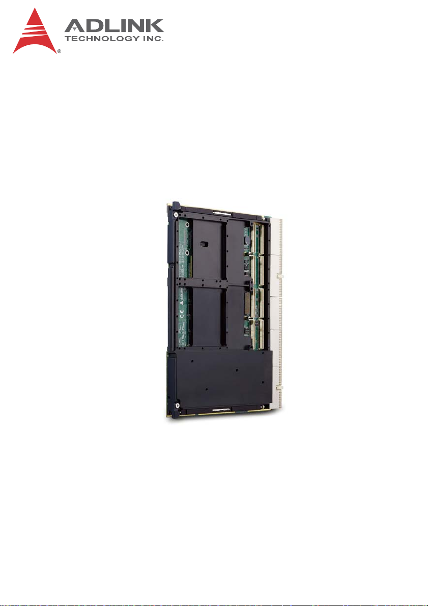
CT-61
Rugged Conduction Cooled Low Power 6U CompactPCI
Processor Blade with Intel® Core™ i7 and Two PMC Sites
User’s Manual
Manual Rev. 1.00
Revision Date: September 25, 2014
Part No: 50-1Y002-1000
Advance Technologies; Automate the World.
Page 2

Revision History
Revision Release Date Description of Change(s)
1.00 2014/09/25 Initial release
Page 3

CT-61
Preface
Copyright 2014 ADLINK Technology Inc.
This document contains proprietary infor mation protected by copyright. All rights are reserved. No part of this manual may be reproduced by any mechanical, electronic, or other means in any form
without prior written permission of the manufacturer.
Disclaimer
The information in this document is subject to change without prior
notice in order to improve reliability, design, and function and does
not represent a commitment on the part of the manufa cturer.
In no event will the manufacturer be liable for direct, indirect, special, incidental, or consequential damages arising out of the use or
inability to use the product or documentation, even if advised of
the possibility of such damages.
Environmental Responsibility
ADLINK is committed to fulfill its social responsibility to global
environmental preservation through compliance with the European Union's Restriction of Hazardous Substances (RoHS) directive and Waste Electrical and Electronic Equipment (WEEE)
directive. Environmental protection is a top priority for ADLINK.
We have enforced measures to ensure that our products, manufacturing processes, components, and raw materials have as little
impact on the environment as possible. When products are at their
end of life, our customers are encouraged to dispose of them in
accordance with the product disposal and/or recovery programs
prescribed by their nation or company.
Trademarks
Product names mentioned herein are used for identification purposes only and may be trademarks and/or registered trademarks
of their respective companies.
Preface iii
Page 4
Conventions
Take note of the following conventions used throughout this
manual to make sure that users perform certain tasks and
instructions properly.
Additional information, aids, and tips that help users perform
tasks.
NOTE:
NOTE:
Information to prevent minor physical injury, component damage, data loss, and/or program corruption when trying to com-
CAUTION:
WARNING:
plete a task.
Information to prevent serious physical injury, component
damage, data loss, and/or program corruption when trying to
complete a specific task.
iv Preface
Page 5

CT-61
Table of Contents
Revision History...................................................................... ii
Preface.................................................................................... iii
List of Tables......................................................................... vii
List of Figures........................................................................ ix
1 Overview ............................................................................. 1
1.1 Introduction.......................................................................... 1
1.2 Features............................................................................... 2
1.3 Block Diagram ..................................................................... 3
1.4 Product List............................. ... .......................................... 4
2 Specifications..................................................................... 5
2.1 CT-61 Specifications............................................................ 5
2.2 Power Requirements.................... ... .... ... ... ... ... .... ... ... ... .... ... 7
2.3 Thermal Management Features .......................................... 9
3 Functional Description .................................................... 11
3.1 Processor........................................................................... 11
3.2 Chipset............................................................................... 12
3.3 Super I/O ........................................................................... 13
3.4 Battery ............................................................................... 13
3.5 PMC/XMC Sites................................................................. 13
3.6 BIOS Recovery.................................................... .............. 14
4 Board Interfaces............................................................... 15
4.1 CT-61 Board Layout - Top Side......................................... 15
4.2 CT-61 Board Layout - Bottom Side.................................... 16
4.3 Connector Pin Assignments .............................................. 17
4.4 Switch and Jumper Settings.............................................. 25
Table of Contents v
Page 6

5 Getting Started.................................................................. 29
5.1 CT-61 Blade Installation..................................................... 29
5.2 PMC/XMC Module Installation........................................... 30
6 Driver Installation.............................................................. 31
6.1 Driver Installation Procedure.............................................. 31
7 Utilities............................................................................... 33
7.1 Watchdog Timer................................................................. 33
7.2 Preboot Execution Environment (PXE).............................. 38
7.3 BIOS Recovery........................ .... ... ... ... .... ... ... ... ... ............. 39
7.4 Programming NT Mode EEPROM Map............................. 41
8 BIOS Setup Utility............................................................. 43
8.1 Starting the BIOS............................................................... 43
8.2 Main Setup......................................................................... 46
8.3 Advanced BIOS Setup....................................................... 47
8.4 Chipset Configuration ........................................................ 57
8.5 Boot Configuration............................................................. 60
8.6 Security Setup.................................................................... 62
8.7 Save & Exit ........................................................................ 63
9 IPMI User Guide ................................................................ 65
9.1 Introduction........................................................................ 65
9.2 Summary of Commands Supported by BMR-AVR-cPCI... 65
9.3 OEM Commands Summary Table............ ... ... ... ... ....... ... ... 69
9.4 CompactPCI Address Map ................................................ 73
9.5 Communications with IPMC............................................... 74
9.6 IPMI Sensors List............................................................... 74
9.7 Relevant Documents................................. ... ... ... ... .... ... ... ... 74
Important Safety Instructions............................................... 75
Getting Service...................................................................... 77
vi Table of Contents
Page 7

CT-61
List of Tables
Table 2-1: CT-61 Specifications ................................................ 6
Table 2-2: CompactPCI Input Voltage Characteristics .............. 7
Table 2-3: Idle Mode Power Consumption ................................ 8
Table 2-4: 100% CPU Usage Power Consumption ................... 8
Table 4-1: XMC Connector Pin Definition ................................ 17
Table 4-2: PMC Connector Pin Definitions .............................. 18
Table 4-3: CompactPCI J1 Connector Pin Definition ............... 20
Table 4-4: CompactPCI J2 Connector Pin Definition ............... 21
Table 4-5: CompactPCI J3 Connector Pin Definition ............... 22
Table 4-6: CompactPCI J4 Connector Pin Definition ............... 23
Table 4-7: CompactPCI J5 Connector Pin Definition ............... 24
Table 4-8: Mode Switch Settings .. ... ... ... .... ... ... ... ... .... ... ... ... .... . 26
Table 4-9: PMC Bandwidth/Clock Switch Settings .................. 26
List of Tables vii
Page 8

This page intentionally left blank.
viii List of Tables
Page 9

CT-61
List of Figures
Figure 1-1: CT-61 Block Diagram ................................................ 3
Figure 4-1: CT-61 Board Layout - Top Side............................... 15
Figure 4-2: CT-61 Board Layout - Bottom Side ......................... 16
List of Figures ix
Page 10

This page intentionally left blank.
xList of Figures
Page 11

1Overview
1.1 Introduction
The CT-61 is a conduction cooled 6U CompactPCI single board
computer in single slot width (4HP) form factor supporting 32nm
Intel® Core™ i7 SV, LV, ULV processors with integrated graphics
and ECC memory controller onboard. The CT-61 provides up to
8GB of dual channel DDR3-800/1066 ECC memory soldered
onboard and implements the Mobile In tel® QM57 Express Chipset
to provide a full feature set and optimal performance per watt.
The CT-61 provides a 64bit/66MHz CompactPCI bus, up to two
PMC sites with 64-bit/133MHz PCI-X bus supporting rear I/O
(PIM), and one PCI Express x8 XMC site (shared with inner PMC
site). Rear I/O provides versatile additional I/O including two
PICMG 2.16 GbE, USB, COM, High Definition Audio, and SATA
interfaces.
For flexibility of use, the CT-61 can be installed in a standard CompactPCI system slot as system master, or peripheral slot as a PCI
device. Through hardware switch setting, the CT-61 optionally
supports operation in system or per ipheral slots as a standalone
blade. The CT-61 is ideally suited for military, aviation, communication and other industrial applications.
CT-61
Overview 1
Page 12

1.2 Features
X 6U CompactPCI SBC in 4HP width form factor
X µFC-BGA package Intel® Core™ i7 processor, up to 2.53GHz
X Mobile Intel® BD82QM57 PCH (Platform Controller Hub)
X Dual Channel DDR3 ECC SDRAM at 800 or 1066MHz sol-
dered onboard, up to 8GB
X 64-bit/66MHz CompactPCI Interface based on PCI specifica-
tions, 3.3V and 5V signaling
X Supports operation in system slot as system master or in
peripheral slot with connectivity to CompactPCI bus* (optional
isolation from CompactPCI bus)
X Dual PMC sites with 64-bit/133MHz PCI bus
X Single XMC site with PCIe x8 lane (shared with inner PMC
site)
X -40°C to 85°C operating temperature (at wedge locks)
X RTM models available with multiple I/O options: SATA, HD
audio, COM, USB, Gigabit Ethernet, PS/2 KB/MS, PIM, SAS,
SCSI, CF, SD socket
X Hardware RAID on SCSI, SAS interfaces supported (depen-
dent on RTM module)
*See “Programming NT Mode EEPROM Map” on page 41 for
instructions on how to set the PCIe-to-PCI bridge on the CT-61
NOTE:
NOTE:
to NT-mode to allow operation in a peripheral slot.
2Overview
Page 13
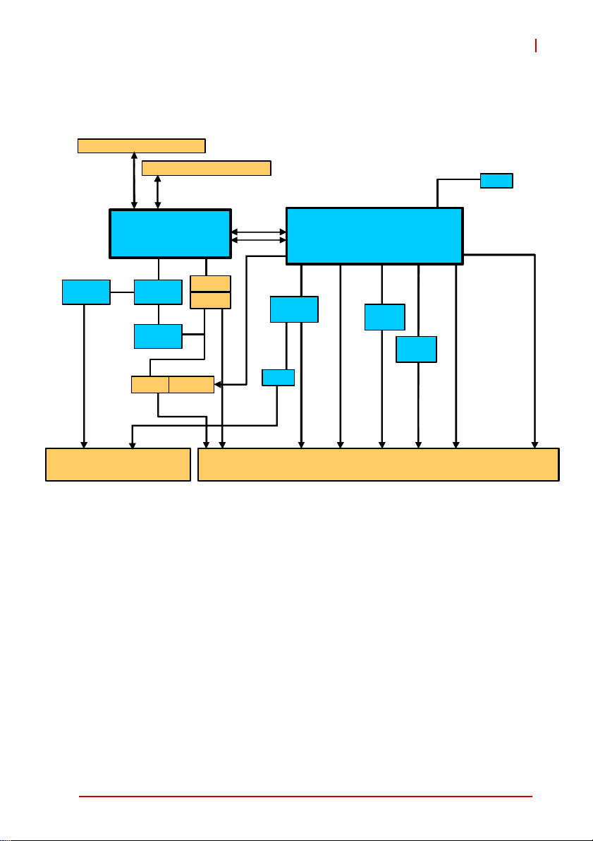
1.3 Block Diagram
Soldered w/ ECC, max. 4GB
Soldered w/ ECC, max. 4GB
DDR3 800/10 66
SPI
CT-61
BIOS
Pericom
PI7C9X13
PCI 64b/66M
Intel® Cor e™i7
PCIe x8
PCIe
Switch
PCIe x4
PCIe x4
Pericom
PI7C9X13
PCI-X 64b/133M
PMC 2
Rear I/O
XMC
PMC 1
2.5” HDD
PCIe x8
Rear I/O
DMI
SATA1
COM4
IPMB 0/1
ITE8783
BMC
SIO
LPC
KB/MS
2x COM
J1/J2 J3/J4/J5
Figure 1-1: CT-61 Block Diagram
QM57 PCH
Intel
82574L
6x USB
3x SAT A
HDA
5x GPIO
RTC
PCIe x4
LVDS
Intel
82574L
PCIe x1 PCIe x1
GbE3 GbE4
TMDSB
RGB
Overview 3
Page 14

1.4 Product List
Products included in the CT-61 include:
Processor Blade
X CT-61: 4HP width (single-slot) 6U CompactPCI blade fea-
turing single Intel® Core™i7 processor, dual channel
DDR3-800/1066 soldered onboard SDRAM with ECC,
2x PMC
Rear Transition Modules
X cPCI-R6002: 4HP width RTM with DVI-I, 2x COM, 3x USB, 2x
GbE, 2xSATA
X cPCI-R6100: 4HP width RTM with 4x GbE, 4x USB, 2xSATA,
DVI, VGA, PS/2 KB/MS, CF & SD sockets
X cPCI-R6110: 4HP width RTM with 2x GbE, 4x USB, 3x SATA,
VGA, PS/2 KB/MS, CF, & SD sockets
X cPCI-R6200: 8HP width RTM with 2x GbE, 2x COM, 4x USB,
DVI-I, 3x SATA, Mic-in, Line-out, PS/2 KB/MS, 8x SAS
X cPCI-R6210: 4HP width RTM with 2xUSB, DVI-I, COM,
2x SATA, 2x PIM
The contents of non-standard CT-61 configurations may vary
depending on customer requests.
NOTE:
NOTE:
This product must be protected from static discharge and physical shock. Never remove any of the components except at a
CAUTION:
4Overview
static-free workstation. Use the anti-static bag shipped with the
product when putting the board on a surface. Wear an
anti-static wrist strap properly grounded on one of the system's
ESD ground jacks when installing or servicing system components.
Page 15

2 Specifications
2.1 CT - 61 Specifications
PICMG® 2.0 CompactPCI® Rev. 3.0
CompactPCI
Standard
Mechanical
Processor
Chipset Intel® QM57 Platform Controller Hub (PCH)
Memory
CompactPCI Bus
PMC/XMC
Graphics
Ethernet
Serial Ports Two serial ports routed to rear I/O
BIOS AMI® EFI BIOS 64Mbit SPI flash memory
PICMG® 2.1 Hot Swap Specification Rev.2.0
PICMG® 2.9 System Management Bus Rev. 1.0
PICMG® 2.16 Packet Switching Backplane Rev.1.0
Standard 6U CompactPCI®
Board size: 233.23 mm x 160mm
Single slot (4HP, 20.32mm) width
CompactPCI® connectors J1, J2, J3, J4 and J5
µFC-BGA Intel® Core™i7-610E, 4MB L2 cache, 2.53GHz
µFC-BGA Intel® Core™i7-620LE, 4MB L2 cache, 2.0GHz
µFC-BGA Intel® Core™i7-620UE, 4MB L2 cache, 1.06GHz
Dual channel DDR3-800/1066 soldered onboard SDRAM
with un-buffered ECC
DDR3-800 for Core™i7-620UE processor
DDR3-1067 for Core™i7-610E/620LE processors
Maximum 8GB capacity
PCI 64-bit/ 66MHz; V(I/O) 3.3V and 5V signaling
Supports operation in system slot or in peripheral slot with
connectivity to CompactPCI bus (Universal Mode)
Optional Satellite mode by switch setting
Two PCI 64-bit/133MHz PMC sites, V(I/O) 3.3V (contact
ADLINK for 5V support)
One PCIe x8 XMC site (shared with inner PMC site)
Integrated in Intel® Core™i7 processor
Analog RGB signal to rear
DVI port routed to rear
Supports dual independent display
Analog RGB up to QXGA
PCIe x1 Intel® 82574L GbE controllers
Two 10/100/1000BASE-T ports to J3
CT-61
1
Specifications 5
Page 16

Supports PICMG® 2.9 secondary system management bus
IPMI functions implemented as defined by IPMI Spec. v1.5 ;
IPMI Interface
ATmega128L-8AU Baseboard Management Controller
(BMC) with 128KB programmable in-system flash, 4KB
EEPROM, and 4KB internal SDRAM
Microsoft® Windows® 7 Ultimate
Microsoft® Windows® Vista Enterprise
Supported OS
Microsoft® Windows® XP Professional SP3
Fedora™ 12
Other OS support upon request
Operating
Temperature
Storage
temperature
-40°C to +85°C at wedge lock
-40°C to 85°C
Humidity 20% to 95% non-condensing
Shock 20G peak-to-peak, 11ms duration, non-operating
Vibration Operating: 20Grms. 5 to 500Hz, each axis
Compliance CE EN55022, FCC Class A
T able 2-1: CT-61 Specifications
Notes:
1. See 7.4 "Programming NT Mode EEPROM Map" on page 41
for instructions on how to set the PCIe-to-PCI bridge on the
CT-61 to Non-Transparent mode to allow operation in a peripheral slot.
Specifications are subject to change without prior notice.
NOTE:
NOTE:
6 Specifications
Page 17

CT-61
2.2 Power Requirements
In order to guarantee a stable functionality of the system, it is recommended to provide more power than the system requires. An
industrial power supply unit should be able to provide at least
twice as much power as the entire system requires of each
voltage. An ATX power supply unit should be able to provide at
least three times as much power as the entire system requires.
The tolerance of the voltage lines described in the CompactPCI
specification (PICMG 2.0 R3.0) is +5%/ -3% for 5, 3.3 V and ±5%
for ±12V. This specification is for power delivered to each slot an d
it includes both the power supply and the backplane tolerance.
Voltage
5V +5.0 VDC +5% / -3% 50 mV
3.3V +3.3 VDC +5% / -3% 50 mV
+12V +12 VDC +5% / -5% 240 mV
-12V -12 VDC +5% / -5% 240 mV
V I/O (PCI I/O
Buffer Voltage)
GND
Table 2-2: Comp actPCI Input Voltage Characteristics
Nominal
Value
+3.3 VDC or
+5 VDC
Tolerance
+5% / -3% 50 mV
Max. Ripple
(P - P)
Specifications 7
Page 18
Power Consumption
This section provides information on the power consumption of the
CT-61 with different CPUs, 2GB DDR3-800/1066 soldered memory, and 100GB SATA HDD. The system was tested in Idle Mode
and Full Load Mode under Windows XP running Burn-in Test 6.0.
The CT-61 is powered by 5V and 3.3V.
Idle Mode under Windows XP
CPU Core™ i7 610E Core™ i7 620LE Core™ i7 620UE
Voltage
+3.3 4.19 13.82 4.12 18.41 3.85 12.71
Total 19.51 23.76 17.96
100% CPU Usage under Windows XP
CPU Core™ i7 610E Core™ i7 620LE Core™ i7 620UE
Voltage
+3.3 6.09 20.10 5.83 19.25 5.31 17.52
Total 42.31 37.08 27.87
Current
(V)
+5 1.14 5.69 1.07 5.35 1.05 5.25
(V)
+5 4.44 22.21 3.57 17.83 2.07 10.35
(A)
Table 2-3: Idle Mode Power Consumption
Current
(A)
Power
(W)
Power
(W)
Current
(A)
Current
(A)
Power
(W)
Power
(W)
Current
(A)
Current
(A)
Power
(W)
Power
(W)
T able 2-4: 100% CPU Usage Power Consumption
8 Specifications
Page 19

CT-61
2.3 Thermal Management Features
When the CPU temperature exceed s its maximum junction temperature (T
reduce power consumption (and thus performance) in an attempt
to reduce the core junction temperature. Use of the CPU’s thermal
management features is intended for short periods of time when
running power intensive applications. If the system is operated
under conditions below the TDP curves above, activation of the
thermal management features will be minimal and reduction in
CPU performance will be minor.
However, if the operating conditions are outside the limits set out
above, the CPU temperature may exceed T
periods, resulting in noticeable performance loss and reduced reliability of the processor.
In extreme situations, the thermal management features may be
incapable of cooling the processor. If the CPU temperature
exceeds approximately 130°C, a catastrophic cooling failure will
be detected and the processor will automatically shut down to prevent physical damage to the processor.
), the CPU’s thermal management features will
j,Max
for prolonged
j,Max
Prolonged operation above the CPU’s maximum junction temperature (Tj,Max=105°C) may damage the CPU and/or reduce
WARNING:
Specifications 9
its long term reliability. Be sure to follow the thermal guidelines
set out in this document.
Page 20

This page intentionally left blank.
10 Specifications
Page 21

3 Functional Description
The following sections describe the CT-61 features and functions.
3.1 Processor
Intel® Core™ i7 Processor
The Intel® Core™ i7-620LE/UE and i7-610E are 64-bit, multi-core
mobile processors built on a 32 nanometer process technology.
The processors are designed for a two-chip platform consisting of
a processor and the Platform Controller Hub (PCH) and enables
higher performance, lower cost, easier validation, and improved
x-y footprint. The Intel® Core™ i7-620LE/UE and i7-610E processors are offered in a BGA1288 package and include an integrated
graphics and memory controller die on the same package as the
processor core die.
The following table lists the processors supported by the CT-61
and their specifications.
Features SV Core i7-610E LV Core i7-620LE ULV Core i7-620UE
Clock 2.53GHz 2.0GHz 1.06GHz
Max. Turbo Freq. 3.2GHz 2.8GHz 2.13GHz
L2 cache 4MB 4MB 4MB
Max. Power (TDP1)
2
T
j,Max
Process 32nm 32nm 32nm
# of cores/threads 2/4 2/4 2/4
Notes:
1. The highest expected sustainable power while running known
power intensive applications. TDP is not the maximum power
that the processor can dissipate.
2. Maximum junction temperature (T
ported operating temperature.
35W 25W 18W
105°C 105°C 105°C
). The maximum sup-
j,Max
CT-61
Functional Description 11
Page 22

System Memory Support
X Two channels of DDR3 memory soldered onboard
X Memory DDR3 data transfer rates of 800 and 1066 MT/s
X 64-bit wide channels (72-bit wide including ECC)
X Supports ECC unbuffered DDR3 memory
X Theoretical maximum memory bandwidth of:
Z
12.8 GB/s in dual-channel mode assuming DDR3 800 MT/s
Z
17.1 GB/s in dual-channel mode assuming DDR3 1066 MT/s
X 1-Gb and 2-Gb DDR3 DRAM technologies for x8 devices
X Using 2Gb device technologies, the largest memory capac-
ity is 8GB
3.2 Chipset
Mobile Intel® QM57 Express Chipset
The CT-61 incorporates the Mobile Intel® QM57 Express Chipset,
also referred to as PCH (Platform Controller Hub), to provide
extensive I/O support. Functions and capabilities include:
X PCI Express Base 2.0 Specification support for up to eight
ports
X 4 PCI Express x1 connected to LAN controllers
X 4 PCI Express x1 are configured to PCI Express x4 and
routed to J5 for I/O expansion
X ACPI Power Management Logic Support
X Two integrated SATA host controllers with up to six ports,
supporting independent DMA operation and dat a transfer
rates of up to 3.0GB/s (the CT-61 supports up to four SATA
ports)
X Supports Advanced Host Controller Interface (AHCI)
X Intel Rapid Storage Technology provides high performance
RAID 0, 1, 5, and 10 functionality
X High speed USB 2.0 allows data transfers up to 480 Mb/s
X Provides Intel Virtualization Technology with Directed I/O
(Intel VT-d) support.
12 Functional Description
Page 23

CT-61
3.3 Super I/O
The ITE IT8783F Super I/O is on a Low Pin Count interface supporting PS/2 keyboard/mouse, 16C550-compatible serial ports,
floppy drive interface, hardware monitor function to monitor CPU
voltage, CPU temperature, power supply voltages and system temperature, and Watchdog Timer with time resolution from minimum 1
second or minute to maximum 65,535 se co nd s or minutes.
3.4 Battery
The CT-61 is p ro vided with a 3.0V/0.2F gold ca p for th e Rea l Time
Clock (RTC). The gold cap supports a 12-hour theoretically life.
3.5 PMC/XMC Sites
The CT-61 supports two PMC sites for front panel I/O expansion.
The PMC sites provides a maximum 64bit/133MHz PCI-X bus link
using a Pericom PI7C9X130 PCIe-to-PCI bridge and PCIe x4 link.
The PMC/XMC sites support +3.3V signaling and 5V VPWR by
default. For optional 5V signaling and 12V VPWR support, contact
your ADLINK sales representative.
The JN1/5 and JN2/6 connectors provide the signals for the 32-bit
PCI bus. The JN3/7 connector provides the 64 bit extension for the
PMC interface. The JN3/7 connectors support user defined I/O
signals and are routed to the CompactPCI J4/5 connectors to rear
I/O.
The CT-61 provides a PCIe x8 XMC interface sharing the same
space as the inner PMC site for high speed I/O e xpansion, such as
10GbE or high-end graphics.
Functional Description 13
Page 24

3.6 BIOS Recovery
The CT-61 features AMI® EFI BIOS with BIOS recovery. If the
BIOS becomes corrupted and you are unable to boot your system,
follow the instructions in Section 7.3 “BIOS Recovery” on page 39.
14 Functional Description
Page 25
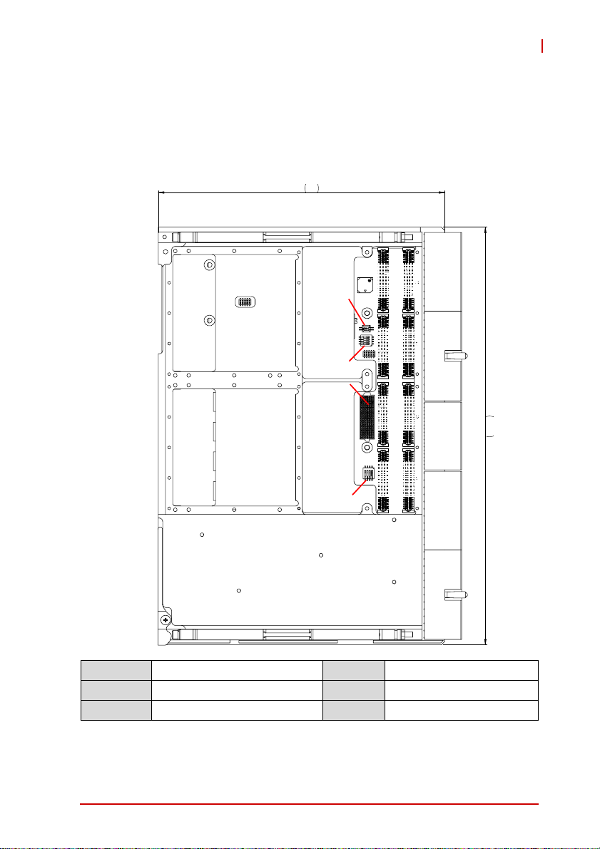
4 Board Interfaces
This chapter describes the board layout, connector pin assignments, and jumper settings of the CT-61.
4.1 CT-61 Board Layout - Top Side
160
CT-61
JN5 JN7
J5
JN6 JN8
SW1
J4
SW2
CN8
JN1 JN3
JN2 JN4
J3
SW3
J2
J1
CN8 XMC conne ctor SW1 Reserved
J1-5 CompactPCI connectors SW2 Mode Switch
JN1-8 PMC connectors SW3 PMC Clock Switch
233.2
Figure 4-1: CT-61 Board Layout - Top Side
Board Interfaces 15
Page 26

4.2 CT- 61 Board Layout - Bottom Side
SW6 SW4
SW4 Reserved SW6 Clear CMOS
Figure 4-2: CT-61 Board Layout - Bottom Side
16 Board Interfaces
Page 27
CT-61
4.3 Connector Pin Assignments
Refer to “CT-61 Board Layout - Top Side” on page 15 and “CT-61
Board Layout - Bottom Side” on page 16 for connector locations.
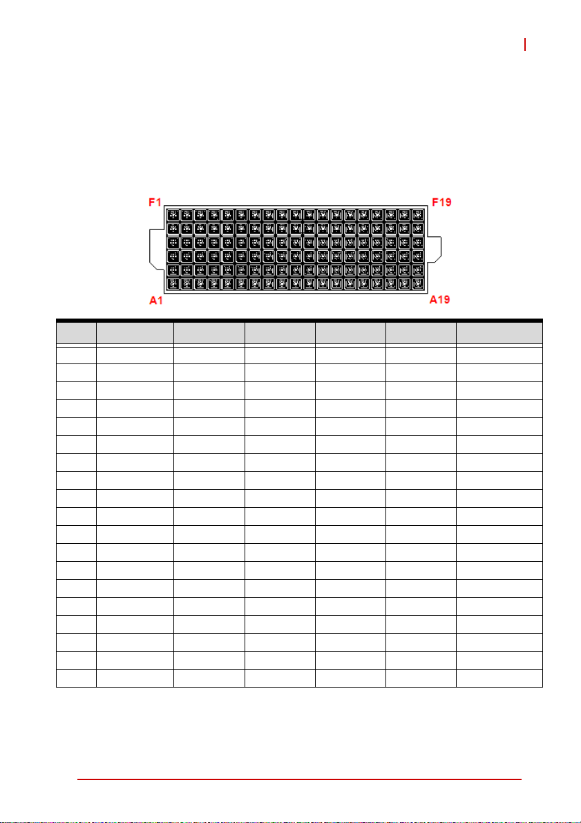
XMC Connector (CN8)
Pin# A B C D E F
1 PETp0 PETn0 3.3V PETp1 PETn1 VPWR
2 GND GND TRST# GND GND MRSTI#
3 PETp2 PETn2 3.3V PETp3 PETn3 VPWR
4 GND GND TCK GND GND MRSTO#
5 PETp4 PETn4 3.3V PETp5 PETn5 VPWR
6 GND GND TMS GND GND +12V
7 PETp6 PETn6 3.3V PETp7 PETn7 VPWR
8 GND GND TDI GND GND -12V
9NC NCNCNCNCVPWR
10 GND GND TDO GND GND GA0
11 PERp0 PERn0 MBIST# PERp1 PERn1 VPWR
12 GND GND GA1 GND GND MPRESENT#
13 PERp2 PERn2 3.3V AUX PERp3 PERn3 VPWR
14 GND GND GA2 GND GND MSDA
15 PERp4 PERn4 NC PERp5 PERn5 VPWR
16 GND GND MVMRO GND GND MSCL
17 PERp6 PERn6 NC PERp7 PERn7 NC
18 GND GND NC GND GND NC
19 REFCLK+0 REFCLK-0 NC WAKE# ROOT0# NC
Table 4-1: XMC Connector Pin Definition
Board Interfaces 17
Page 28

PMC Connector (JN1/5, JN2/6, JN3/7, JN4/8)
Pin# JN1/5 Signal JN2/6 Signal JN3/7 Signal JN4/8 Signal
1 PMC_TCK P12V NC PIO1
2 N12V PMC_TRST-L GND PIO2
3 GND PMC_TMS GND PIO3
4 PCIX_INTA-L NC (PMC_TDO) PCIX_CBE-L7 PIO4
5 PCIX_INTB-L PMC_TDI PCIX_CBE-L6 PIO5
6 PCIX_INTC-L GND PCIX_CBE-L5 PIO6
7 PMC_MOD-L1 GND PCIX_CBE-L4 PIO7
8P5V NC GND PIO8
9 PCIX_INTD-L NC PMC_VIO PIO9
10 NC NC PCIX_PAR64 PIO10
11 GND PMC_MOD-L2 PCIX_AD63 PIO11
12 P3V3_PMCAUX P3V3 PCIX_AD62 PIO12
13 CLK66_PCIX_PMC PMC_RST-L PCIX_AD61 PIO13
14 GND PMC_MOD-L3 GND PIO14
15 GND P3V3 GND PIO15
16 PCIX_GNT-L0 PMC_MOD-L4 PCIX_AD60 PIO16
17 PCIX_REQ-L0 PMC_PME-L PCIX_AD59 PIO17
18 P5V GND PCIX_AD58 PIO18
19 PMC_VIO PCIX_AD30 PCIX_AD57 PIO19
20 PCIX_AD31 PCIX_AD29 GND PIO20
21 PCIX_AD28 GND GND PIO21
22 PCIX_AD27 PCIX_AD26 PCIX_AD56 PIO22
23 PCIX_AD25 PCIX_AD24 PCIX_AD55 PIO23
24 GND PCIX_AD23 PCIX_AD54 PIO24
25 GND PMC_IDSEL PCIX_AD53 PIO25
26 PCIX_CBE-L3 PCIX_AD23 GND PIO26
27 PCIX_AD22 P3V3 GND PIO27
28 PCIX_AD21 PCIX_AD20 PCIX_AD52 PIO28
29 PCIX_AD19 PCIX_AD18 PCIX_AD51 PIO29
30 P5V GND PCIX_AD50 PIO30
31 PCIX_FRAME-L PCIX_AD16 PCIX_AD49 PIO31
32 PCIX_AD17 PCIX_CBE-L2 GND PIO32
6364
12
Table 4-2: PMC Connector Pin Definitions
18 Board Interfaces
Page 29

Pin# JN1/5 Signal JN2/6 Signal JN3/7 Signal JN4/8 Signal
33 PCIX_FRAME-L GND GND PIO33
34 GND NC PCIX_AD48 PIO34
35 GND PCIX_TRDY-L PCIX_AD47 PIO35
36 PCIX_IRDY-L P3V3 PCIX_AD46 PIO36
37 PCIX_DEVSEL-L GND PCIX_AD45 PIO37
38 P5V PCIX_STOP-L GND PIO38
39 PCIX_PCIXCAP PCIX_PERR-L GND PIO39
40 PCIX_LOCK-L GND PCIX_AD44 PIO40
41 NC P3V3 PCIX_AD43 PIO41
42 NC PCIX_SERR-L PCIX_AD42 PIO42
43 PCIX_PAR PCIX_CBE-L1 PCIX_AD41 PIO43
44 GND GND GND PIO44
45 PMC_VIO PCIX_AD14 GND PIO45
46 PCIX_AD15 PCIX_AD13 PCIX_AD40 PIO46
47 PCIX_AD12 PCIX_M66EN PCIX_AD39 PIO47
48 PCIX_AD11 PCIX_AD10 PCIX_AD38 PIO48
49 PCIX_AD9 PCIX_AD8 PCIX_AD37 PIO49
50 P5V P3V3 GND PIO50
51 GND PCIX_AD7 GND PIO51
52 PCIX_CBE-L0 NC PCIX_AD36 PIO52
53 PCIX_AD6 P3V3 PCIX_AD35 PIO53
54 PCIX_AD5 NC PCIX_AD34 PIO54
55 PCIX_AD4 NC PCIX_AD33 PIO55
56 GND GND GND PIO56
57 PMC_VIO NC GND PIO57
58 PCIX_AD3 NC PCIX_AD32 PIO58
59 PCIX_AD2 GND NC PIO59
60 PCIX_AD1 NC NC PIO60
61 PCIX_AD0 PCIX_ACK64-L NC PIO61
62 P5V P3V3 GND PIO62
63 GND GND GND PIO63
64 PCIX_REQ64-L NC NC PIO64
Table 4-2: PMC Connector Pin Definitions (cont’d)
CT-61
Board Interfaces 19
Page 30

CompactPCI J1 Connector Pin Assignment
Pin Z A B C D E F
1 GND +5V -12V TRST# +12V +5V GND
2 GND TCK# +5V TMS# NC TDI# GND
3 GND IRQA# IRQB# IRQC# +5V IRQD# GND
4 GND +5V_IPMB HEALTHY# V(I/O) NC NC GND
5 GND NC NC RESET# GND GNT0# GND
6 GND REQ0# GND +3.3V CLK0 AD31 GND
7 GND AD30 AD29 AD28 GND A D27 GND
8 GND AD26 GND V(I/O) AD25 AD24 GND
9 GND CBE3# IDSEL AD23 GND AD22 GND
10 GND AD21 GND +3.3V AD20 AD19 GND
11 GND AD18 AD17 AD16 GND CBE2# GND
12-14 Key
15 GND +3.3V FRAME# IRDY# BDSEL# TRDY# GND
16 GND DEVSEL# PCIXCAP V(I/O) STOP# LOCK# GND
17 GND +3.3V IPMB_CLK IPMB_DAT GND PERR# GND
18 GND SERR# GND +3.3V PAR CBE1# GND
19 GND +3.3V AD15 AD14 GND AD13 GND
20 GND AD12 GND VIO AD11 AD10 GND
21 GND +3.3V AD9 AD8 M66EN CBE0# GND
22 GND AD7 GND +3.3V AD6 AD5 GND
23 GND +3.3V AD4 AD3 +5V AD2 GND
24 GND AD1 +5V V(I/O) AD0 ACK64# GND
25 GND +5V REQ64# ENUM# +3.3V +5V GND
Table 4-3: CompactPCI J1 Connector Pin Definition
20 Board Interfaces
Page 31

CT-61
CompactPCI J2 Connector Pin Assignment
Pin Z A B C D E F
1 GND CLK1 GND REQ1# GNT1# REQ2# GND
2 GND CLK2 CLK3 SYSEN# GNT2# REQ3# GND
3 GND CLK4 GND GNT3# REQ4# GNT4# GND
4 GND V(I/O) NC CBE7# GND CBE6# GND
5 GND CBE5# GND V(I/O) CBE4# PAR64 GND
6 GND AD63 AD62 AD61 GND AD60 GND
7 GND AD59 GND V(I/O) AD58 AD57 GND
8 GND AD56 AD55 AD54 GND AD53 GND
9 GND AD52 GND V(I/O) AD51 AD50 GND
10 GND AD49 AD48 AD47 GND AD46 GND
11 GND AD45 GND V(I/O) AD44 AD43 GND
12 GND AD42 AD41 AD40 GND AD39 GND
13 GND AD38 GND V(I/O) AD37 AD36 GND
14 GND AD35 AD34 AD33 GND AD32 GND
15 GND NC GND FAL# REQ5# GNT5# GND
16 GND NC NC DEG# GND NC GND
17 GND NC GND RSTBTN# REQ6# GNT6# GND
18 GND NC NC NC GND NC GND
19 GND GND GND NC NC NC GND
20 GND CLK5 GND NC GND NC GND
21 GND CLK6 GND NC NC NC GND
22 GND GA4 GA3 GA2 GA1 GA0 GND
Table 4-4: CompactPCI J2 Connector Pin Definition
Board Interfaces 21
Page 32

CompactPCI J3 Pin Assignment
Pin Z A B C D E F
1GNDHDA_RST# HDA_SYNC HDA_BIT_CLK HDA_SDOUT HDA_SDIN0 GND
2GND
3GND
4GND
5 GND GND GND NC GND GND GND
6GND
7GND
8GND
9GND
10 GND
11 GND
12 GND
13 GND
14 GND
15 GND
16 GND
17 GND
18 GND
19 GND P5V P5V P12V P5V P5V GND
HDA_SDIN1 HDA_SDIN2 NC
KBDATA KBCLK NC MSDATA MSCLK GND
SATA-TX4+ SATA-TX4- GND SATA-TX3+ SATA-TX3- GND
SATA-RX4+ SATA-RX4- GND SATA-RX3+ SATA-RX3- GND
COM4-TX COM4-RX COM3-DCD# IPMB_CLK IPMB_DAT GND
COM3-RX COM3-TX COM3-DTR# COM3-DSR# COM3- RTS# GND
COM3-CTS# COM3-RI# RGB-BLUE RGB-RED RGB-GREEN GND
USB-OC3# RGB-DDCCLK RGB-DDCDAT RGB-HSYNC RGB-VSYNC GND
USB-P3+ USB-P3- GND USB-P4+ USB-P4- GND
USB-P5+ USB-P5- GND USB-P6+ USB-P6- GND
USB-P7+ USB-P7- GND USB-P8+ USB-P8- GND
USB-OC4# USB-OC5# USB-OC6# USB-OC7# USB-OC8# GND
LAND_TXD1+ LAND_TXD1- GND LAND_TXD3+ LAND_TXD3- GND
LAND_TXD0+ LAND_TXD0- GND LAND_TXD2+ LAND_TXD2- GND
LANC_TXD1+ LANC_TXD1- GND LANC_TXD3+ LANC_TXD3- GND
LANC_TXD1+ LANC_TXD0- GND LANC_TXD2+ LANC_TXD2- GND
HDA_DOCK_EN#
HAD_DOCK_RST#
GND
Table 4-5: CompactPCI J3 Connector Pin Definition
High Definition audio
Keyboard/Mouse
Serial ATA
Serial ports
USB ports
Ethernet ports
RGB
22 Board Interfaces
Page 33

CT-61
CompactPCI J4 Connector Pin Assignment
Pin Z A B C D E F
1 GND NC PMC1 IO:64 PMC1 IO:63 PMC1 IO:62 PMC1 IO:61 GND
2 GND PMC1 IO:60 PMC1 IO:59 PMC1 IO:58 PMC1 IO:57 PMC1 IO:56 GND
3 GND PMC1 IO:55 PMC1 IO:54 PMC1 IO:53 PMC1 IO:52 PMC1 IO:51 GND
4 GND PMC1 IO:50 PMC1 IO:49 PMC1 IO:48 PMC1 IO:47 PMC1 IO:46 GND
5 GND PMC1 IO:45 PMC1 IO:44 PMC1 IO:43 PMC1 IO:42 PMC1 IO:41 GND
6 GND PMC1 IO:40 PMC1 IO:39 PMC1 IO:38 PMC1 IO:37 PMC1 IO:36 GND
7 GND PMC1 IO:35 PMC1 IO:34 PMC1 IO:33 PMC1 IO:32 PMC1 IO:31 GND
8 GND PMC1 IO:30 PMC1 IO:29 PMC1 IO:28 PMC1 IO:27 PMC1 IO:26 GND
9 GND PMC1 IO:25 PMC1 IO:24 PMC1 IO:23 PMC1 IO:22 PMC1 IO:21 GND
10 GND PMC1 IO:20 PMC1 IO:19 PMC1 IO:18 PMC1 IO:17 PMC1 IO:16 GND
11 GND PMC1 IO:15 PMC1 IO:14 PMC1 IO:13 PMC1 IO:12 PMC1 IO:11 GND
12-14 Key
15 GND PMC1 IO:10 PMC1 IO:9 PMC1 IO:8 PMC1 IO:7 PMC1 IO:6 GND
16 GND PMC1 IO:5 PMC1 IO:4 PMC1 IO:3 PMC1 IO:2 PMC1 IO:1 GND
17 GND NC PMC2 IO:64 PMC2 IO:63 PMC2 IO:62 PMC2 IO:61 GND
18 GND PMC2 IO:60 PMC2 IO:59 PMC2 IO:58 PMC2 IO:57 PMC2 IO:56 GND
19 GND PMC2 IO:55 PMC2 IO:54 PMC2 IO:53 PMC2 IO:52 PMC2 IO:51 GND
20 GND PMC2 IO:50 PMC2 IO:49 PMC2 IO:48 PMC2 IO:47 PMC2 IO:46 GND
21 GND PMC2 IO:45 PMC2 IO:44 PMC2 IO:43 PMC2 IO:42 PMC2 IO:41 GND
22 GND PMC2 IO:40 PMC2 IO:39 PMC2 IO:38 PMC2 IO:37 PMC2 IO:36 GND
23 GND PMC2 IO:35 PMC2 IO:34 PMC2 IO:33 PMC2 IO:32 PMC2 IO:31 GND
24 GND PMC2 IO:30 PMC2 IO:29 PMC2 IO:28 PMC2 IO:27 PMC2 IO:26 GND
25 GND PMC2 IO:25 PMC2 IO:24 PMC2 IO:23 PMC2 IO:22 PMC2 IO:21 GND
Table 4-6: CompactPCI J4 Connector Pin Definition
Board Interfaces 23
Page 34

CompactPCI J5 Pin Assignment
Pin Z A B C D E F
1GNDPCIE-TX0+ PCIE-TX0- GND PCIE-RX0+ PCIE-RX0- GND
2GND
3GND
4GND
5 GND GND GND GND GND GND GND
6GND
7 GND GND GND RTC GND GND GND
8GND
9GND
10 GND
11 GND
12 GND
13 GND
14 GND PMC2 IO:20 PMC2 IO:19 GND
15 GND PMC2 IO:18 PMC2 IO:17 GPIO6
16 GND PMC2 IO:16 PMC2 IO:15 GPIO7 PMC2 IO:14 PMC2 IO:13 GND
17 GND PMC2 IO:12 PMC2 IO:11 GPIO8 PMC2 IO:10 PMC2 IO:9 GND
18 GND PMC2 IO:8 PMC2 IO:7 DETECT# PMC2 IO:6 PMC2 IO:5 GND
19 GND PMC2 IO:4 PMC2 IO:3 NC PMC2 IO:2 PMC2 IO:1 GND
20 GND
21 GND
22 GND NC
PCIE-TX1+ PCIE-TX1- GND PCIE-RX1+ PCIE-RX1- GND
PCIE-TX2+ PCIE-TX2- GND PCIE-RX2+ PCIE-RX2- GND
PCIE-TX3+ PCIE-TX3- GND PCIE-RX3+ PCIE-RX3- GND
PCIE-CLK+ PCIE-CLK- G ND RESET# NC GND
LVDS_DATA3- LVDS_DATA3+ NC LVDS_CLK LVDS_DATA GND
GPIO1 GPIO2 GPIO3 GPIO4 GPIO5 GND
TDC0+ TDC0- GND TDC1+ TDC1- GND
TDC2+ TDC2- GND TLC+ TLC- GND
DVI_DATA DVI_CLK DVI_HTPLG NC NC GND
LAND_100# LANC_100# NC LANC_1G# LAND_1G# GND
SATA-TX5+ SATA-TX5- GND
SATA-RX5+ SATA-RX5- GND
LVDS_DATA0- LVDS_DATA0+ GND LVDS_DATA1- LVDS_DATA1+ GND
LVDS_DATA2- LVDS_DATA2+ GND LVDS_CLK- LVDS_CLD+ GND
LAND_LINK_ACT#
+3.3V
LANC_LINK_ACT#
+3.3V GND
Table 4-7: CompactPCI J5 Connector Pin Definition
PCI-Express x4
GPIO
DVI
Ethernet port
LVDS
Serial ATA
24 Board Interfaces
Page 35

4.4 Switch and Jumper Settings
Refer to “CT-61 Board Layout - Top Side” on page 15 and “CT-61
Board Layout - Bottom Side” on page 16 for switch locations.
SW1 & SW4 (Debug use only)
The switches SW1 & 4 are for debugging purposes and should
be left in the default settings. The default setting of SW1 is all
OFF; the default setting of SW4 is Pin 1 OFF and Pin 2 ON.
Mode Switch (SW2)
Switch SW2 is a multi purpose switch that allows users to
define the board operating mode. Four pins independently control the mode setting. All are set to OFF by default.
Pin# Status Description
Universal Mode:
bus communication with the host board in the system slot. The
OFF
CT-61 can boot-up in a peripheral slot and be recognized by the
1
2
host board in the system slot as a PCI device.
Satellite Mode:
CompactPCI bus communication with the host board in the system
ON
slot. The CT-61 behaves a as standalone blade in the peripheral
slot.
When the system does not include a CMM (Chassis
OFF
Management
"without CMM mode".
When the system includes a CMM, set this pin to ON to allow
ON
IPMI to run in "with CMM mode".
The CT-61 in a peripheral slot has CompactPCI
The CT-61 in a peripheral slot has no
Module), set this pin to OFF to allow IPMI to run in
CT-61
Board Interfaces 25
Page 36

Pin# Status Description
OFF
3
OFF
4
The CT-61 cannot boot-up when installed in a peripheral slot if
there is no host board in the system slot.
The CT-61 is able to boot-up when installed in a peripheral slot if
there is no host board in the system slot. The CT-61 behaves as a
ON
system board in all slots. (Set this pin to "ON" if the CT-61 is
installed in a blade server backplane).
The CT-61 power on/off is state is controlled by the ejector handle
state.
ON
Force the ejector handle state to "closed".
Table 4-8: Mode Switch Settings
PMC Bandwidth/Clock Switch (SW3)
Switch SW3 allows the user to force the PCI bus to lower bandwidth and clock settings. All are set OFF by default to support
PCI-X mode up to 64bit/133MHz maximum with the bandwidth
and clock determined by the PCI device attached.
PIN ON OFF
1 Force the PCI bandwidth to 32bit
2 Force the PCI clock to 66MHz
Force the PCI bus to PCI mode
3
(no PCI-X mode support)
Force the PCI clock to
4
PCI-X 100MHz
Table 4-9: PMC Bandwidth/Clock Switch Settings
26 Board Interfaces
Auto Negotiation
Page 37

CT-61
Clear CMOS Switch (SW6)
Press switch SW6 to clear the CMOS and reset the CMOS values to default.
Board Interfaces 27
Page 38

This page intentionally left blank.
28 Board Interfaces
Page 39

5 Getting Started
This chapter describes the installation of the following component s
to the CT-61.
X CT-61 Blade installation
X PMC/XMC module installation
5.1 CT-61 Blade Installation
1. Carefully align the edges of the blade with the edges of
the slot.
2. Check that all the wedge locks lie flat against the board.
3. Slide the blade into the slot.
4. Tighten the wedge locks using a hex torque screwdriver
set to 6.0 ±0.5 kgf·cm (0.59 ±0.05 N·m).
To remove the cond uc tio n- co ole d bla d e, use th e fo llo wing steps:
1. Loosen the wedge locks using a hex screwdriver.
2. Use the ejection levers to disengage the lock.
CT-61
3. Carefully remove the blade from the conduction-cooled
chassis.
Getting Started 29
Page 40

5.2 PMC/XMC Module Installation
The CT-61 provides one PMC and one PMC/XMC slot. The
PMC/XMC slots support 3.3V V(I/O) and 5V VPWR only. For
optional 5V V(I/O) and 12V VPWR support, please contact
ADLINK.
Installing a PMC/XMC Module
1. Align the male connectors of the PMC/XMC card (component-side down) to the female connectors of the
CT-61 and press down.
2. Secure th e PMC/XMC card to the CT-61 by attaching the
screws provided with the card from the bottom side of
the board.
30 Getting Started
Page 41

6 Driver Installation
The CT-61 drivers can be found on the ADLINK All-In-One CD at
X:\cPCI\CT-61\ or from the ADLINK website (http://www.adlinktech.com). ADLINK provides validated drivers for chipset, graph-
ics and LAN on Windows XP Professional, Windows Vista, and
Windows 7.
6.1 Driver Installation Procedure
The following describes the driver installation procedures for Windows XP.
1. Install the Windows operating system before installing
any driver. Most standard I/O device drivers are installed
during Windows installation.
2. Install the chipset driver by extracting and running the pro-
gram in ...\Chipset\
Intel_INF_Update_Utility_WinAllOS_v9.1.1.1023.zip.
3. Install the graphics driver and utilities by extracting and run-
ning the program in ...\Graphics\
Intel_Graphics_Adapter_WinXP32_v6.14.10.5237.zip.
4. Install the LAN drivers by extracting and running the pro-
gram in
…\LAN\Intel_Network_Adapter_WinXP32_v11.4.7.0.zip.
We recommend using the drivers provided on the ADLINK
All-in-One CD or downloading them from the ADLINK website to
ensure compatibility. The Vxw orks BSP can be downloaded from
the CT-61 product page on the ADLINK website
(http://www.adlinktech.com).
CT-61
Driver Installation 31
Page 42

This page intentionally left blank.
32 Driver Installation
Page 43

7 Utilities
7.1 Watchdog Timer
This section describes the operation of the CT-61’s watchdog
timer (WDT). The primary function of the WDT is to monitor the
CT-61's operation and to reset the system if a software application
fails to function as programmed. The following WDT functions may
be controlled using a software application:
X enabling and disabling
X reloading timeout value
The CT-61 custom WDT circuit is implemented using the internal
IO of the ITE Super I/O IT8783 which is at address 2Eh of LPC.
The basic functions of the WDT include:
X Starting the timer countdown
X Enabling or disabling WDT
X Enabling or disabling WDT countdown LED ON
X Reloading the timeout value to keep the watchdog from timing
out
X Setting the range of the timeout period from 1 to 15300 seconds
or minutes
X Sending a RESET signal to the system when the watchdog
times out
CT-61
Using the Watchdog in an Application
The following section describes using the WDT functions in an
application. The WDT reset function is explained in the previous
section. This can be controlled through the registers in the CT-61's
Super I/O.
An application using the reset fe ature enab les the watch dog func tion, sets the count-down period, and reloads the timeout value
periodically to keep it from resetting the system. If the timer countdown value is not reloaded, the watchdog resets the system hardware after its counter reaches zero.
Utilities 33
Page 44

For a detailed programming sample, refer to the sample code provided on the ADLINK All-In-One CD. You can find it in the following
directory: X:\cPCI\CT-61\WDT.
Sample Code
The sample program written in C shown below offers an interactive
way to test the Watchdog Timer under DOS.
#include<stdio.h>
#include<dos.h>
#define IT8783_ID1 0x87
#define IT8783_ID2 0x83
static unsigned int IT8783_ioPort = 0x2e;
//Check index port
void Enter_IT8783_Config(unsigned int flag)
{
if(flag) IT8783_ioPort = 0x4e;
switch(IT8783_ioPort)
{
case 0x2E: //Address port = 0x2E, enter keys =
0x87, 0x01, 0x55, 0x55
outportb(0x2E, 0x87);
outportb(0x2E, 0x01);
outportb(0x2E, 0x55);
outportb(0x2E, 0x55);
break;
case 0x4E: //Address port = 0x4E, enter keys =
0x87, 0x01, 0x55, 0xAA
outportb(0x4E, 0x87);
outportb(0x4E, 0x01);
outportb(0x4E, 0x55);
outportb(0x4E, 0xAA);
break;
default:
break;
}
}
34 Utilities
Page 45

CT-61
//Exit index port
void Exit_IT8783_Config(unsigned int flag)
{
if(flag) IT8783_ioPort = 0x4e;
outportb(IT8783_ioPort, 0x02);
outportb(IT8783_ioPort+1, 0x02);
}
//Check chip
void Get_IT8783_ID(unsigned int &ID1, unsigned int &ID2)
{
outportb(IT8783_ioPort, 0x20);
ID1 = inportb(IT8783_ioPort+1);
outportb(IT8783_ioPort, 0x21);
ID2 = inportb(IT8783_ioPort+1);
}
//WDT and LED program
void IT8783_3_WDTRun(unsigned int count_value, unsigned
int PLEDflag) //for CT-61
{
unsigned long tempCount;
unsigned int registerValue;
outportb(IT8783_ioPort, 0x07);
outportb(IT8783_ioPort+1, 0x07);// Device 7
outportb(IT8783_ioPort, 0xf8);
outportb(IT8783_ioPort+1, 0x00);// PLED mapping to
nothing, disable PLED function
if(PLEDflag == 1)
{
outportb(IT8783_ioPort, 0x2D);
registerValue = inportb(IT8783_ioPort + 1);
registerValue |= 0x01; // set Pin109 is
GPIO function GP60
outportb(IT8783_ioPort+1, registerValue);
outportb(IT8783_ioPort, 0xC5);
registerValue = inportb(IT8783_ioPort + 1);
Utilities 35
Page 46

registerValue &= 0xfe; // set GP60 is
alternate function
outportb(IT8783_ioPort+1, registerValue);
outportb(IT8783_ioPort, 0xCD);
registerValue = inportb(IT8783_ioPort + 1);
registerValue |= 0x01; // set GP60 is output
outportb(IT8783_ioPort+1, registerValue);
outportb(IT8783_ioPort, 0xf8);
outportb(IT8783_ioPort+1, 0x30);// PLED
mapping to GP60
outportb(IT8783_ioPort, 0xf9);
registerValue = inportb(IT8783_ioPort + 1);
registerValue |= 0x02;
registerValue &= 0xfb;
outportb(IT8783_ioPort+1, registerValue);
}
outportb(IT8783_ioPort, 0x71);
registerValue = inportb(IT8783_ioPort + 1);
registerValue |= 0xD0; // set Mouse & Keyboard
interrupt Enable
outportb(IT8783_ioPort+1, registerValue);
outportb(IT8783_ioPort, 0x73);
outportb(IT8783_ioPort+1, count_value);
// set WDT count LSB
tempCount = tempCount >> 8;
outportb(IT8783_ioPort, 0x74);
outportb(IT8783_ioPort+1, count_value);
// set WDT count MSB
if(count_value >= 60)
{
outportb(IT8783_ioPort, 0x72);
registerValue = inportb(IT8783_ioPort+1);
registerValue &= 0x8f;
registerValue |= 0x10; //enable WDT output
through PowerOK!
outportb(IT8783_ioPort+1, registerValue);
// set WDT count is minute
36 Utilities
Page 47

tempCount = count_value / 60;
if((count_value%60) > 30)
tempCount++;
if(tempCount > 65535)
tempCount = 65535;
printf("WDT timeout in %d minutes.\n",
tempCount);
}
else
{
outportb(IT8783_ioPort, 0x72);
registerValue = inportb(IT8783_ioPort+1);
registerValue |= 0x80;
tempCount = count_value;
if(tempCount != 0)
{
printf("WDT timeout in %d seconds.\n",
tempCount);
registerValue |= 0x40; //Enable WDT
output through KBRST
}
else
{
printf("WDT is Disabled.\n");
registerValue &= 0xbf; //Disable WDT
output through KBRST
}
CT-61
outportb(IT8783_ioPort+1, registerValue);
// set WDT count is second
}
}
Utilities 37
Page 48

7.2 Preboot Execution Environment (PXE)
The CT-61 supports the Intel® Preboot Execution Environment
(PXE) that is capable of booting up or executing an OS installation
through an Ethernet port. To use PXE, there must be a DHCP
server on the network with one or more servers running PXE and
MTFTP services. It could be a Windows® 2003 server running
DHCP, PXE, and MTFTP services or a dedicated DHCP server
with one or more additional servers running PXE and MTFTP services.
To build a network environment with PXE support:
1. Setup a DHCP server with PXE tag configuration
2. Install the PXE and MTFTP services
3. Make a boot image file on the PXE server (i.e. the boot server)
4. Enable the PXE boot function on the client computer
38 Utilities
Page 49

CT-61
7.3 BIOS Recovery
The CT-61 features AMI® EFI BIOS with BIOS recovery. If the
BIOS becomes corrupted and you are unable to boot your system,
the system will sound 4 beeps. Follow the instructions below to
re-flash the BIOS and recover the system.
1. Download the BIOS recovery file “C6510000.ROM” from the
product website at :
detail.php?cKind=&pid=1017
2. Prepare a bootable USB flash drive and copy the recovery file “C6510000.ROM” to the root directory.
3. Insert the USB flash drive into the CT-61 and power up
the system.
4. The system will sound 4 beeps to indicate boot failure,
and then it will sound 2 beeps to indicate it is entering
Recovery Mode. You will see the screen below:
http://www.adlinktech.com/PD/web/PD_
5. Select “Proceed with flash update” and press Enter.
Utilities 39
Page 50

6. During the BIOS recovery process, you will see the following:
7. Af ter the flash update is completed, power down the syste m
and restart. The system should now boot up normally.
40 Utilities
Page 51

CT-61
7.4 Programming NT Mode EEPROM Map
The CT-61 supports operation in peripheral slot as PCI device with
PCI bus communication with the system board (Universal Mode).
To operate in a peripheral slot in Non-Transparent mode, the
PCIe-to-PCI bridge on the CT-61 should be set to Non-Transparent
mode by programming the NT mode EEPROM map. The EEPROM
map can be downloaded from the CT-61 product page on the
ADLINK website:
http://www.adlinktech.com/PD/web/PD_detail.php?cKind=&pid=1017
To set the PCIe-to-PCI bridge on the CT-61 to NT mode, perform
the following steps:
1. Download the EERPOM map cPCI-6510_NT.rar from
the CT-61 product website under Utilities.
2. Prepare a bootable USB flash drive and extract the con-
tents of the folder cPCI-6510_NT into the root directory.
3. Insert the USB flash drive into the CT-61 in system slot
and power up the system.
4. Execute the file NT.bat to program the bridge to
Non-Transparent mode. The board will then operate in a
peripheral slot as a PCI device.
5. To return the CT-61 to Transparent mode, execute the
file TR.bat.
Utilities 41
Page 52

This page intentionally left blank.
42 Utilities
Page 53

8 BIOS Setup Utility
The following chapter describes basic navigation for the
AMIBIOS®8 BIOS setup utility.
8.1 Starting the BIOS
To enter the setup screen, follow these steps:
1. Power on th e motherboard
2. Press the < Delete > key on your keyboard when you
see the following text prompt:
< Press DEL to run Setup >
3. After you press the < Delete > key, the main BIOS setup
menu displays. You can access the other setup screens
from the main BIOS setup menu.
CT-61
Note: In most cases, the < Delete > key is used to invoke the setup
screen. There are several cases that use other keys, such as
< F1 >, < F2 >, and so on.
BIOS Setup Utility 43
Page 54

Setup Menu
The main BIOS setup menu is the first screen that you can navigate. Each main BIOS setup menu option is described in this
user’s guide.
The Main BIOS setup menu screen has two main frames. The left
frame displays all the options that can be configured. “Grayed”
options cannot be configured, “Blue” options can be.
The right frame displays the key legend. Above the key legend is
an area reserved for a text message. When an option is selected
in the left frame, it is highlighted in white. Often a text message will
accompany it.
44 BIOS Setup Utility
Page 55

CT-61
Navigation
Note: There is a hot key legend located in the right frame on most
setup screens.
Keyboard Commands
Enter Selects the highlighted option or submenu.
< > The Left and Right “Arrow” keys allow you to select a setup
screen.
^ v The Up and Down “Arrow” keys allow you to select a setup
screen.
+ - The Plus and Minus keys allow you to change the field value
Tab Moves the cursor to the next configurable item or to the next
Esc The Esc key allows you to discard any changes you ha ve
BIOS Setup Utility 45
of a particular setup item.
field.
made and exit the Setup menu. Press the Esc key to exit
the Setup menu without saving your changes. Press the
Enter key to discard changes and exit. You can also use the
“Arrow” keys to select Cancel and then press the Enter key
to abort this function and return to the previous screen.
Page 56

8.2 Main Setup
When you first enter the Setup Utility , you will enter the Main setup
screen. You can always re turn to the Ma in setup screen by selecting the Main tab. There are two Main Setup options. They are
described in this section. The Main BIOS Setup screen is shown
below.
System Language
Choose the system default language.
System Time/System Date
Use this option to change the system time and date. Highlight System Time or System Date using the < Arrow > keys. En ter new values using the keyboard. Press the < Tab > key or the < Arrow >
keys to move between fields. The date must be entered in
MM/DD/YY format. The time is entered in HH:MM:SS format.
Note: The time is in 24-hour format. For example, 5:30 A.M. ap-
46 BIOS Setup Utility
pears as 05:30:00, and 5:30 P.M. as 17:30:00.
Page 57

CT-61
8.3 Advanced BIOS Setup
Select the Advanced tab from the setup screen to enter the
Advanced BIOS Setup screen. You can select any of the items in
the left frame of the screen, such a s SuperIO Conf iguration, to go
to the sub menu for that item. You can display an Advanced BIOS
Setup option by highlighting it using the < Arrow > keys. The
Advanced BIOS Setup screen is shown below.
The sub menus are described on the following pages.
Launch PXE OpROM
Boot option for legacy network devices. Options: LAN1, LAN2,
LAN3, LAN4, Disabled.
Launch Storage OpROM
Boot option for legacy mass storage devices with Option ROM.
Options: Enabled/Disabled.
BIOS Setup Utility 47
Page 58

PCI Subsystem Settings
PCI Latency Timer
Value to be programmed into PCI Latency Timer Register.
Options: 32 PCI Bus Clocks, 64 PCI Bus Clocks, 96 PCI Bus
Clocks, 128 PCI Bus Clocks, 160 PCI Bus Clocks, 192 PCI Bus
Clocks, 224 PCI Bus Clocks, 248 PCI Bus Clocks.
ASPM Support
Set the ASPM (Active State Power Management) level. Options:
X Disabled: Disable ASPM
X Auto: BIOS auto configure
X Force L0: Force all links to L0 State
48 BIOS Setup Utility
Page 59

CPU Configuration
Hyper-Threading
Enables/disables Hyper-Threading Technology.
Active Processor Cores
Number of cores to enable in each processor package.
Options: All, 1, 2.
CT-61
Intel Virtualization
Enables/disables Intel Virtualization Technology.
Power Technology
Power management feature. Options: Disabled, Energy Efficient,
Custom.
TDC Limit
Turbo-XE Mode Processor TDC Limit in 1/8 A granularity.
0 means use the factory-configured value.
TDP Limit
Turbo-XE Mode Processor TDP Limit in 1/8 W granularity.
0 means use the factory-configured value.
BIOS Setup Utility 49
Page 60

SATA Configuration
SATA Mode
The SATA can be configured as a legacy IDE, RAID and AHCI
mode.
Serial ATA Controller 0
This item specifies whether SATA Controller 0 is initialized in
Compatible or Enhanced mode of operation. The settings are
Disabled, Compatible and Enhanced.
Serial ATA Controller 1
This item specifies whether SATA Controller 1 is initialized in
Compatible or Enhanced mode of operation. The settings are
Disabled, Compatible and Enhanced.
50 BIOS Setup Utility
Page 61

Intel IGD SWSCI OpRegion Configuration
DVMT/FIXED Memory
Select DVMT/FIXED Mode Memory size used by internal
Graphics Device. Options: 128MB, 256MB, Maximum.
IGD – Boot Type
Selects the Video Device(s) to be activated during POST. This
option has no effect if external graphics pr es en t. Op tio ns : CRT,
DVI, TV, CRT+DVI.
CT-61
BIOS Setup Utility 51
Page 62

USB Configuration
Legacy USB Support
Legacy USB Support refers to USB mouse and keyboard support. Normally if this option is not enabled, any attached USB
mouse or keyboard will not become available until a USB compatible operating system is fully booted with all USB drivers
loaded. When this option is enabled, any attached USB mouse
or keyboard can control the system even when there is no USB
driver loaded on the system. Set this value to enable or disable
the Legacy USB Support.
EHCI Hand-off
This is a workaround for OSes without EHCI hand-off support.
The EHCI ownership change should be claimed by the EHCI
driver. Options: En able, Disable.
Device Reset Timeout
USB mass storage device Start Unit command timeout.
52 BIOS Setup Utility
Page 63

Super IO Configuration
Serial Port 1/2/4 Configuration
Sub-menu allows you to Enable/Disable and set the parameters of Serial Ports 1, 2, 4.
CT-61
BIOS Setup Utility 53
Page 64

PC Health Configuration
54 BIOS Setup Utility
Page 65

Console Redirection
The settings specify how the host computer and the remote
computer will exchange data. Both computers should have the
same or compatible settings.
The user can enable one serial port for Console Redirection.
Only one port can be used for Console Redir ecti on at any tim e.
CT-61
BIOS Setup Utility 55
Page 66

Terminal Type
VT-UTF8 is the preferred terminal type for out-of-band management. The next best choice is VT100+ and then VT100.
Options: VT100, VT100+, VT-UTF8, ASNI.
Bits per Second
Select the bit rate (bits/second) you want the ser ial port to use
for console redirection. Options: 115200, 57600, 19200, 9600.
Data Bits
Select the data bits you want the serial port to use for console
redirection. Set this value to 7 or 8.
Parity
Set this option to select Parity for console redirection. The settings for this value are None, Even, Odd, Mark, Space.
Stop B its
Stop bits indicate the end of a serial data packet. (A start bit
indicates the beginning). The standard setting is 1 stop bit.
Communication with slow devices may require more than 1
stop bit. Set this value to 1 or 2.
Flow Control
Set this option to select Flow Control for console redirection.
The settings for this value are None, Hardware, Software.
Terminal Resolution
Remote Terminal Resolution. Options: 80x25, 100x31.
56 BIOS Setup Utility
Page 67

CT-61
8.4 Chipset Configuration
Select the Chipset tab from the setup screen to enter the Chipset
BIOS Setup screen. You can select any of Chipset BIOS Setup
options by highlighting it using the < Arrow > keys. The Chipset
BIOS Setup screen is shown below.
Memory Information and Display Configuration
BIOS Setup Utility 57
Page 68

Initial Graphic Adapter
Allows you to select which graphics controller to use as the primary boot device. Configuration options: IGD, PCI/IGD,
PCI/PEG, PEG/IGD, PEG/PCI.
IGD Memory
IGD shared memory size. Options: Disabled, 32M, 64M, 128M.
PCH Configuration
SMBus Controller
The SMBus controller. Set this value to Enable/Disable.
Azalia HD Audio
The onboard HDA Controller. Set this value to Enable/Disable.
58 BIOS Setup Utility
Page 69

USB Configuration
All USB Devices
All USB Devices. Set this value to Enabled/Disabled.
EHCI Controller 1
USB 2.0 (EHCI) support. Set this value to Enabled/Disabled.
USB Port
CT-61
USB Port 0~7.Set this value to Enabled/Disabled.
BIOS Setup Utility 59
Page 70

8.5 Boot Configuration
Select the Boot tab from the setup screen to enter the Boot Configuration screen. You can select any of the items in the left frame
of the screen to go to the sub menu for that item. You can display
a Boot Configuration option by highlighting it using the < Arrow >
keys. The Boot Configuration screen is shown below:
Quiet Boot
When this feature is enabled, the BIOS will display the OEM logo
during the boot-up sequence, hiding normal POST messages.
When it is disabled, the BIOS will display the normal POST messages, instead of the OEM logo.
Fast Boot
Enabling this setting will cause the BIOS Power-On Self Test routine to skip some of its tests during bootup for faster system boot.
Setup Prompt Timeout
Number of seconds to wait for setup activation key. 65535
(0xFFFF) means indefinite waiting.
60 BIOS Setup Utility
Page 71

CT-61
Bootup Num-Lock
This option sets the Num Lock status when the system is powered
on. Setting it to On will turn on the Num Lock key when the system
is booted up. Setting it to Off will not enable the Num Lock key on
bootup.
GateA20 Active
Upon Request: GA20 can be disabled using BIOS services.
Always: do not allow disabling GA20; this option is useful when
any RT code is executed above 1MB.
Interrupt 19 Capture
Allows Option ROMs to trap Int 19. Set this value to Enabled or
Disabled.
Boot Option #1
Set the boot device options to determine the sequence in which
the computer checks which device to boot from.
BBS Priorities
Selects the boot devices available for each device type to be used
for Boot Option Priorities settings.
BIOS Setup Utility 61
Page 72

8.6 Security Setup
Administrator Password
Use this option to set a password for administrators with full control of the BIOS setup utility.
User Password
Use this option to set a password for users with limited access to
the BIOS setup utility.
62 BIOS Setup Utility
Page 73

CT-61
8.7 Save & Exit
Select the Save & Exit tab from the setup screen to enter the Sa ve
& Exit setup screen. You can display a Save & Exit BIOS setup
option by highlighting it using the < Arrow > keys. The Save & Exit
BIOS setup screen is shown below.
Save Changes and Reset
When you have completed the system configuration changes,
select this option to leave Setup and reboot the computer so the
new system configuration parameters can take effect.
Discard Changes and Reset
Select this option to quit Setup without making any permanent
changes to the system configuration.
Restore Defaults
Restore/Load Defaults values for all the setup options.
Boot Override
Use the up/down arrow keys to highlight a boot device to immediately exit the BIOS Setup and boot from the selected device.
BIOS Setup Utility 63
Page 74

This page intentionally left blank.
64 BIOS Setup Utility
Page 75

9 IPMI User Guide
9.1 Introduction
This chapter is written for those who already have a basic understanding of the newest implementation of the baseboard management controller (BMC) of the Intelligent Platform Management
Interface (IPMI) specification rev. 2.0. It also describes the OEM
extension IPMI command usages which are not listed in the IPMI
specification.
9.2 Summary of Commands Supported by
BMR-AVR-cPCI
The table below lists all the commands supported by the
BMR-AVR-cPCI. For detailed information on supported commands, please refer to the Intelligent Platform Management Interface Specification downloadable from the Intel we bsite
(http://www.intel.com/design/servers/ipmi/spec.htm).
CT-61
Command
IPM Device “Global” Commands
Get Device ID 20.1 App 0 1h
Cold Reset 20.2 App 02h
Warm Reset 20.3 App 03h
Get Self Test
Results
Get Device GUID 20.8 App 08h
IPMI User Guide 65
IPMI
Spec
NetFn CMD Description
20.4 App 04h
This command is used to retrieve the
Intelligent Device’s Hardware Revision,
Firmware/Software Revision, and Sensor
and Event Interface Command
specification revision information.
This command directs the Responder to
perform a ‘Cold Reset’ of itself.
This command directs the Responder to
perform a ‘Warm Reset’ of itself.
This command directs the device to
return its Self Test results, if any.
This command returns a GUID (Globally
Unique ID), also referred to as a UUID
(Universally Unique IDentifier), for the
management controller.
Page 76

Command
Broadcast “Get
Device ID”
IPMI Messaging Support Commands
Send Message 22.7 App 34h
BMC Watchdog Timer
Reset Watchdog
Timer
Set Watchdog
Timer
Get Watchdog
Timer
Event Commands
Set Event Receiver 29.1 S/E 00h
Get Event Receiver 29.2 S/E 01h
Platform Event
Message
IPMI
Spec
NetFn CMD Description
20.9 App 01h
27.5 App 22h
27.6 App 24h
27.7 App 25h
29.3 S/E 02h
This is a broadcast version of the ‘Get
Device ID’ command that is provided for
the ‘discovery’ of Intelligent Devices on
the IPMB
The Send Message command is us ed for
bridging IPMI messages between
channels, and between the system
management software (SMS) and a given
channel.
The Reset Watchdog Timer command is
used for starting and restarting the
Watchdog Timer from the initial
countdown value that was specified in the
Set Watchdog Timer command.
The Set Watchdog Timer command is
used for initializing and configuring the
watchdog timer. The command is also
used for stopping the timer.
This command retrieves the current
settings and present countdown of the
watchdog timer.
This global command tells a controller
where to send Event Messages.
This global command is used to retrieve
the present setting for the Event Receiver
Slave Address and LUN. This command
is only applicable to management
controllers that act as IPMB Event
Generators.
This command may be thought of as a
request for the BMC to process the event
data that the command contains.
Typically, the data will be logged to the
System Event Log (SEL).
66 IPMI User Guide
Page 77

CT-61
Command
Sensor Device Commands
Get Device SDR
Info
Get Device SDR 35.3 S/E 21h
Reserve Device
SDR Repository
Set Sensor
Hysteresis
Get Sensor
Hysteresis
Set Sensor
Threshold
Get Sensor
Threshold
Set Sensor Event
Enable
Get Sensor Event
Enable
Get Sensor Event
Status
IPMI
Spec
35.10 S/E 28h
35.11 S/E 29h
35.13 S/E 2Bh
NetFn CMD Description
35.2 S/E 20h
35.4 S/E 22h
35.6 S/E 24h
35.7 S/E 25h
35.8 S/E 26h
35.9 S/E 27h
This command returns general
information about the collection of
sensors in a Dynamic Sensor Device.
The ‘Get Device SDR’ command allows
SDR information for sensors for a Sensor
Device (typically implemented
in a satellite management controller) to
be returned.
This command is used to obtain a
Reservation ID.
This command provides a mechanism for
setting the hysteresis values associated
with the thresholds of a sensor
that has threshold based event
generation.
This command retrieves the present
hysteresis values for the specified
sensor.
This command is used to set the
specified threshold for the given sensor.
This command retrieves the threshold for
the given sensor.
This command provides the ability to
disable or enable Event Message
Generation for individual sensor events.
The command is also used to enable or
disable sensors in their entirety using the
disable scanning bit.
This command returns the enabled/
disabled state for Event Message
Generation from the selected sensor. The
command also returns the enabled/
disabled state for scanning on the sensor.
The Get Sensor Event Status command
is provided to support systems where
sensor polling is used in addition to, or
instead of, Event Messages for event
detection.
IPMI User Guide 67
Page 78

Command
Get Sensor
Reading
Get Sensor Type 35.16 S/E 2Fh
FRU Device Commands
Get FRU Inventory
Area Info
Read FRU Data 34.2
Write FRU Data 34.3
IPMI
Spec
35.14 S/E 2Dh
NetFn CMD Description
34.1
Stora
ge
Stora
ge
Stora
ge
10h
11h
12h
This command returns the present
reading for sensor. The sensor device
may return a stored version of a
periodically updated reading, or the
sensor device may scan to obtain the
reading after receiving the request.
This command is used to assign the
Sensor Type and Event/Reading Type to
a specified sensor.
Returns overall the size of the FRU
Inventory Area in this device, in bytes.
The command returns the specified data
from the FRU Inventory Info area.
The command writes the specified byte
or word to the FRU Inventory Info area.
68 IPMI User Guide
Page 79

CT-61
9.3 OEM Commands Summary Table
Command NetFn Code Cmd Code
OemShowRevision OEM (C0h) 12h
OemRescanGaInput OEM (C0h) 22h
OemTestFunction OEM (C0h) 30h
OemSetBlueLEDLongBlinking OEM (C0h) 31h
OemReportGeoAddress OEM (C0h) F0h
OemEnableSmbus OEM (C0h) F2h
OemDisableSmbus OEM (C0h) F3h
OemDispDebugVariable OEM (C0h) F4h
OemResetHost OEM (C0h) F5h
OemPowerOff OEM (C0h) F6h
OemPowerOn OEM (C0h) F7h
OemShowRevision
This command is used to show the current information of the firmware including the firmware revision, the product ID, and addi-
tional features.
Action Byte Value Description
Request
Response
IPMI User Guide 69
0 C0h NetFn/LUN for OEM
1 12h OEM defined command
0 Complete Code 00h means OK
1 A5h Internal check byte. Always A5h
2 *Firmware Rev ‘V’ in ASCII code for verification
3 *Firmware Rev Revision info high byte
4 *Firmware Re v Revision info low byte
5 *Product ID ‘P’ in ASCII code for verification
6 *Product ID Product info high byte
7 *Product ID Product info low byte
8 *Special info ‘S’ in ASCII code for verification
9 *Special info Addition info byte
10 5Ah Internal check byte. Always 5Ah
Page 80

OemRescanGaInput
This command is used to rescan the geo-address input pins and
reset the IPMB address according to the input value.
Action Byte Value Description
Request
Response
0 C0h NetFn/LUN for OEM
1 22h OEM defined command
0 Complete Code 00h means OK
1 New IPMB address New IPMB address value
OemTestFunction
Internal test purposes only.
OemSetBlueLEDLongBlinking
This command is used to enable or disable the slow blink of the
blue HotSwap LED when a voltage is detected to be over ±5% out
of range for five seconds (see Table 4-1 on page 22).
This function
is set to enabled by default.
Action Byte Value Description
0 C0h NetFn/LUN for OEM
Request
Response 0 Complete Code 00h means OK
1 31h OEM defined command
2 00h or 01h
00h: disable slow blink capability
01h: enable slow blink capability
70 IPMI User Guide
Page 81

OemReportGeoAddress
This command can report the IPMB address, the GA pin input status, and the event forwarding control value.
Action Byte Value Description
Request
Response
0 C0h NetFn/LUN for OEM
1 F0h OEM defined command
0 Complete Code 00h means OK
1 IPMB address IPMB address value
2 GA value GA pin input status
3 Control value Current control value of event forwarding
OemEnableSmbus
This command is used to turn on the I2C bus when it is off during
boot up process. Usually BIOS will perform this command after
booting in boards with ServerWorks chipset.
Action Byte Value Description
Request
Response 0 Complete Code 00h means OK
0 C0h NetFn/LUN for OEM
1 F2h OEM defined command
CT-61
OemDisableSmbus
This command is used to shut down I2C bus access.
Action Byte Value Description
Request
Response 0 Complete Code 00h means OK
IPMI User Guide 71
0 C0h NetFn/LUN for OEM
1 F3h OEM defined command
Page 82

OemDispDebugVariable
This command can report up t o 5 interval values for debug purposes. For developers only.
Action Byte Value Description
Request
Response
0 C0h NetFn/LUN for OEM
1 F4h OEM defined command
0 Complete Code 00h means OK
1 *Debug variable 1
2 *Debug variable 2
3 *Debug variable 3
4 *Debug variable 4
5 *Debug variable 5
OemResetHost
This command is implemented to control the system’s status if
rebooting is required. Operators can control the system remotely.
Action Byte Value Description
Request
Response 0 Complete Code 00h means OK
0 C0h NetFn/LUN for OEM
1 F5h OEM defined command
OemPowerOff
This command is implemented to control the system’s status if
power-off is required. Operators can control the system remotely.
Action Byte Value Description
Request
Response 0 Complete Code 00h means OK
72 IPMI User Guide
0 C0h NetFn/LUN for OEM
1 F6h OEM defined command
Page 83

CT-61
OemPowerOn
This command is implemented to control the system’s status if
power-on is required. Operators can control the system remotely.
Action Byte Value Description
Request
Response 0 Complete Code 00h means OK
0 C0h NetFn/LUN for OEM
1 F7h OEM defined command
9.4 CompactPCI Address Map
Since more than one system may be installed in a single chassis,
we allocate each IPMB address based on GA input as peripheral
cards. The CompactPCI Peripheral Address Mapping Table is
given below.
CompactPCI Peripheral Address Mapping
Geo. Addr. IPMB Addr. Geo. Addr. IPMB Addr.
0Disabled16 D0h
1B0h17D2h
2B2h18D4h
3B4h19D6h
4B6h20D8h
5B8h21DAh
6 Bah 22 DCh
7 BCh 23 DEh
8 BEh 24 E0h
9 Coh 25 E2h
10 C4h 26 E4h
11 C6h 27 E6h
12 C8h 28 E8h
13 CAh 29 EAh
14 CCh 30 ECh
15 CEh 31 Disabled
IPMI User Guide 73
Page 84

9.5 Communications with IPMC
Operating systems need to use a serial port to com municate with
the IPMC. The resource setting of the serial port must be IO:
0x3E8 and IRQ: 3. The communication setting of the serial port
must be BaudRate: 9600, DataBit: 8, ParityCheck: None, StopBit:
1, and FlowControl: None. In Windows XP, use “COM3” to communicate with the IPMC.
9.6 IPMI Sensors List
Sensor
Number
00h BMC Watchdog
01h 3.3V 3.3 V
02h 5V 5 V
03h 12V 12 V
04h SYSTEM Temp 25°C
05h CPU Temp 40°C
06h BIOS CHANGE
07h BIOS POST ERROR
Sensor name
Normal
Reading
9.7 Relevant Documents
Document Title Revision Source
Intelligent Platform
Management Interface
Specification v2.0
PICMG 2.9 D1.0
CompactPCI System
Management Specification
Intelligent Platform
Management Bus
Communications Protocol
Specification v0.9
Document Revision 1.1
February 20, 2002
January 21, 2000
Document Revision 0.15
June 24, 1997
Intel Corp.
http://www.intel.com/design/
servers/ipmi/spec.htm
Intel Corp.
http://www.intel.com/design/
servers/ipmi/license_ipmi.htm
Remark
74 IPMI User Guide
Page 85

CT-61
Important Safety Instructions
For user safety, please read and follow all instructions,
WARNINGS, CAUTIONS, and NOTES marked in this manual
and on the associated equipment before handling/operating the
equipment.
X Read these safety instructions carefully.
X Keep this user’s manual for future reference.
X Read the specifications section of this manual for detailed
information on the operating environment of this equipment.
X When installing/mounting or uninstalling/removing
equipment:
Z Turn off power and u nplug any power cords/cables.
X To avoid electrical shock and/or damage to equipment:
Z Keep equipment away from water or liquid sources;
Z Keep equipment away from high heat or high humidity;
Z Keep equipment properly ventilated (do not block or
cover ventilation openings);
Z Make sure to use recommended voltage and powe r
source settings;
Z Always install and operate equipment near an easily
accessible electrical socket-outlet;
Z Secure the power cord (do not place any obje ct on /ove r
the power cord);
Z Only install/attach and operate equipment on stable
surfaces and/or recommended mountings; and,
Z If the equipment will not be used for long periods of time,
turn off and unplug the equipment from its power source.
Important Safety Instructions 75
Page 86

X Never attempt to fix the equipment. Equipmen t sho u ld on ly
be serviced by qualified personnel.
A Lithium-type battery may be provided for uninterrupted, backup
or emergency power.
Risk of explosion if battery is replaced with one of an incorrect
WARNING:
type. Dispose of used batteries appropriately.
X Equipment must be serviced by authorized technicians
when:
Z The power cord or plug is damaged;
Z Liquid has penetrated the equipment;
Z It has been exposed to high humidity/moisture;
Z It is not functioning or does not function according to the
user’s manual;
Z It has been dropped and/or damaged; and/or,
Z It has an obvious sign of breakage.
76 Important Safety Instructions
Page 87

Getting Service
Contact us should you require any service or assistance.
ADLINK Technology, Inc.
Address: 9F, No.166 Jian Yi Road, Zhonghe District
New Taipei City 235, Taiwan
ᄅקؑխࡉ৬ԫሁ 166 ᇆ 9 ᑔ
Tel: +886-2-8226-5877
Fax: +886-2-8226-5717
Email: service@adlinktech.com
Ampro ADLINK Technology, Inc.
Address: 5215 Hellyer Avenue, #110
San Jose, CA 95138, USA
Tel: +1-408-360-0200
Toll Free: +1-800-966-5200 (USA only)
Fax: +1-408-360-0222
Email: info@adlinktech.com
ADLINK Technology (China) Co., Ltd.
Address: Ϟ⍋Ꮦ⌺ϰᮄᓴ∳催⾥ᡔು㢇䏃 300 ো(201203)
300 Fang Chun Rd., Zhangjiang Hi-Tech Park
Pudong New Area, Shanghai, 201203 China
Tel: +86-21-5132-8988
Fax: +86-21-5132-3588
Email: market@adlinktech.com
CT-61
ADLINK Technology Beijing
Address: ࣫ҀᏖ⍋⎔Ϟഄϰ䏃 1 োⲜ߯ࡼ E ᑻ 801 ᅸ(100085)
Beijing, 100085 China
Tel: +86-10-5885-8666
Fax: +86-10-5885-8626
Email: market@adlinktech.com
ADLINK Technology Shenzhen
Address: ⏅ഇᏖቅ⾥ᡔು催ᮄϗ䘧᭄ᄫᡔᴃು
Tel: +86-755-2643-4858
Fax: +86-755-2664-6353
Email: market@adlinktech.com
LiPPERT ADLINK Technology GmbH
Address: Hans-Thoma-Strasse 11, D-68163
Mannheim, Germany
Tel: +49-621-43214-0
Fax: +49-621 43214-30
Email: emea@adlinktech.com
Rm. 801, Power Creative E, No. 1 Shang Di East Rd.
A1 2 ὐ C (518057)
2F, C Block, Bldg. A1, Cyber-Tech Zone, Gao Xin Ave. Sec. 7
High-Tech Industrial Park S., Shenzhen, 518054 China
Getting Service 77
Page 88

ADLINK Technology, Inc. (French Liaison Office)
Address: 6 allée de Londres, Immeuble Ceylan
91940 Les Ulis, France
Tel: +33 (0) 1 60 12 35 66
Fax: +33 (0) 1 60 12 35 66
Email: france@adlinktech.com
ADLINK Technology Japan Corporation
Address: ͱ101-0045 ᵅҀ䛑ҷ⬄⼲⬄䤯ފ⬎ 3-7-4
Tel: +81-3-4455-3722
Fax: +81-3-5209-6013
Email: japan@adlinktech.com
ADLINK Technology, Inc. (Korean Liaison Office)
Address: 137-881 昢殾柢 昢爎割 昢爎堆嵢 326, 802 (昢爎壟, 微汾瘶捒娯)
Tel: +82-2-2057-0565
Fax: +82-2-2057-0563
Email: korea@adlinktech.com
ADLINK Technology Singapore Pte. Ltd.
Address: 84 Genting Lane #07-02A, Cityneon Design Centre
Tel: +65-6844-2261
Fax: +65-6844-2263
Email: singapore@adlinktech.com
ADLINK Technology Singapore Pte. Ltd. (Indian Liaison Office)
Address: #50-56, First Floor, Spearhead Towers
Malleswaram, Bangalore - 560 055, India
Tel: +91-80-65605817, +91-80-42246107
Fax: +91-80-23464606
Email: india@adlinktech.com
⼲⬄ 374 ɛɳ 4F
KANDA374 Bldg. 4F, 3-7-4 Kanda Kajicho,
Chiyoda-ku, Tokyo 101-0045, Japan
802, Mointer B/D, 326 Seocho-daero, Seocho-Gu,
Seoul 137-881, Korea
Singapore 349584
Margosa Main Road (between 16th/17th Cross)
ADLINK Technology, Inc. (Israeli Liaison Office)
Address: 27 Maskit St., Corex Building
PO Box 12777
Herzliya 4673300, Israel
Tel: +972-77-208-0230
Fax: +972-77-208-0230
Email: israel@adlinktech.com
ADLINK Technology, Inc. (UK Liaison Office)
Tel: +44 774 010 59 65
Email: UK@adlinktech.com
78 Getting Service
 Loading...