

Page 1
CT-31 Series
3U Rugged Conduction-Coole d CompactPCI®
Dual-Core Intel® Atom™ Processor Blade
User’s Manual
Manual Rev.: 2.00
Revision Date: November 15, 2011
Part No: 50-1Y001-1000
Advance Technologies; Automate the World.
Page 2

Revision History
Revision Release Date Description of Change(s)
2.00 2011/11/15 Initial release
ii Revision History
Page 3

CT-31
Preface
Copyright 2011 ADLINK Technology Inc.
This document contains proprietary infor mation protected by copyright. All rights are reserved. No part of this manual may be reproduced by any mechanical, electronic, or other means in any form
without prior written permission of the manufacturer.
Disclaimer
The information in this document is subject to change without prior
notice in order to improve reliability, design, and function and does
not represent a commitment on the part of the manufa cturer.
In no event will the manufacturer be liable for direct, indirect, special, incidental, or consequential damages arising out of the use or
inability to use the product or documentation, even if advised of
the possibility of such damages.
Environmental Responsibility
ADLINK is committed to fulfill its social responsibility to global
environmental preservation through compliance with the European Union's Restriction of Hazardous Substances (RoHS) directive and Waste Electrical and Electronic Equipment (WEEE)
directive. Environmental protection is a top priority for ADLINK.
We have enforced measures to ensure that our products, manufacturing processes, components, and raw materials have as little
impact on the environment as possible. When products are at their
end of life, our customers are encouraged to dispose of them in
accordance with the product disposal and/or recovery programs
prescribed by their nation or company.
Trademarks
Product names mentioned herein are used for identification purposes only and may be trademarks and/or registered trademarks
of their respective companies.
Preface iii
Page 4

Using this Manual
Audience and Scope
The CT-31 User’s Manual is intended for ha rdware te chnicians and
systems operators with knowledge of installing, configuring and
operating CompactPCI systems.
Manual Organization
This manual is organized as follows:
Chapter 1, Introduction: Introduces the CT-31, its features, block
diagrams, and package contents .
Chapter 2, Specifications: Presents detailed specification infor-
mation, power consumption, and technical drawings.
Chapter 3, Functional Description: Describes the CT-31 main
functions.
Chapter 4, Board Interfaces: Describes the CT-31 board inter-
faces.
Chapter 5, Driver Installation: Provides information on how to
install the CT-31 device drivers.
Chapter 6, Utilities: Describes the utilities of the CT-31 Series.
Chapter 7, BIOS Setup: Describes basic navigation for the
AMIBIOS®8 BIOS setup utility.
Important Safety Instructions: Presents safety instructions all
users must follow for the proper setup, installation and usage of
equipment and/or software.
Getting Service: Contact information for ADLINK’s worldwide
offices.
iv Preface
Page 5
CT-31
Conventions
Take note of the following conventions used throughout this
manual to make sure that users perform certain tasks and
instructions properly.
Additional information, aids, and tips that help users perform
tasks.
NOTE:
NOTE:
Information to prevent minor physical injury, component damage, data loss, and/or program corruption when trying to com-
CAUTION:
WARNING:
plete a task.
Information to prevent serious physical injury, component
damage, data loss, and/or program corruption when trying to
complete a specific task.
Preface v
Page 6

This page intentionally left blank.
vi Preface
Page 7

CT-31
Table of Contents
Revision History...................................................................... ii
Preface.................................................................................... iii
List of Figures........................................................................ ix
List of Tables.......................................................................... xi
1 Introduction ........................................................................ 1
1.1 Overview.............................................................................. 1
1.2 Features............................................................................... 1
1.3 Block Diagram ..................................................................... 2
1.4 Product List............................. ... .......................................... 3
1.5 Package Contents ............................................................... 4
2 Specifications..................................................................... 5
2.1 CT-31 Specifications............................................................ 5
2.2 Power Requirements.................... ... .... ... ... ... ... .... ... ... ... .... ... 7
3 Functional Description ...................................................... 9
3.1 Processor............................................................................. 9
3.2 Chipset............................................................................... 12
3.3 Super I/O ........................................................................... 12
3.4 Battery ............................................................................... 12
4 Board Interfaces............................................................... 13
4.1 CT-31 Blade Layout........................................................... 13
4.2 CT-31 Connector Pin Assignments ................................... 15
4.3 CT-31 Switch Settings ....................................................... 19
4.4 DB-3610CF Adapter Board.................................... ... ... .... . 20
4.5 cPCI-R3610T RTM Board Layout...................................... 22
4.6 cPCI-R3610T RTM Connector Pin Assignments............... 23
vii
Page 8

4.7 cPCI-R3610T RTM Switch Settings................................... 27
5 Driver Installation.............................................................. 29
6 Utilities............................................................................... 31
6.1 Watchdog Timer................................................................. 31
7 BIOS Setup........................................................................ 37
7.1 Starting the BIOS............................................................... 37
7.2 Main Setup......................................................................... 41
7.3 Advanced BIOS Setup....................................................... 42
7.3.1 CPU Configuration.........................................................43
7.3.2 IDE Configuration ..........................................................45
7.3.3 Super IO Configuration..................................................46
7.3.4 Hardware Health Configuration .....................................47
7.3.5 USB Configuration.........................................................48
7.3.6 AHCI Configuration.......................... .... ... ... ... ... ..............50
7.3.7 Remote Access Configuration .......................................51
7.4 Advanced PCI/PnP Settings.............................................. 53
7.5 Boot Settings ..................................................................... 54
7.5.1 Boot Settings Configuration...........................................55
7.6 Security Setup.................................................................... 56
7.7 Chipset Setup .................................................................... 59
7.8 Exit Menu........................................................................... 60
Important Safety Instructions............................................... 63
Getting Service...................................................................... 65
viii
Page 9

CT-31
List of Figures
Figure 1-1: CT-31 Series Functional Block Diagram..........................2
Figure 4-1: CT-31 Assembly Layout ................................................13
Figure 4-2: CT-31 PCB Layout......................................................... 14
Figure 4-3: cPCI-R3610T RTM Board Layout..................................22
Figure 4-4: cPCI-R3610T RTM Front Panel.....................................22
List of Figures ix
Page 10

This page intentionally left blank.
xList of Figures
Page 11

CT-31
List of Tables
Table 4-1: CT-31 System LED Descriptions...................................13
Table 4-2: CompactFlash Connector Pin Definition........................ 15
Table 4-3: DB-3610CF Connector Pin Definition............................ 16
Table 4-4: CompactPCI J1 Connector Pin Definition...................... 17
Table 4-5: CompactPCI J2 Connector Pin Definition...................... 18
Table 4-6: VGA/GPIO Mode Switch Settings........ ... ... .... ... ... ... .... .. 19
Table 4-7: USB Connector Pin Definition........................................23
Table 4-8: VGA Connector Pin Definition.................... .... ... ... ... .... .. 23
Table 4-9: GbE Connector Pin Definitions...................................... 24
Table 4-10: Ethernet Status LED Definitions....................................24
Table 4-11: DB-9 Serial Port Connector Pin Definition.....................25
Table 4-12: cPCI-R3610T Serial Port Box Header Pin Definition..... 25
Table 4-13: Serial ATA Connector Pin Definition.. ... ... ... ...................26
Table 4-14: COM2 Mode Selection Switch Settings.........................27
Table 4-15: COM3 Mode Selection Switch Settings.........................28
List of Tables xi
Page 12

This page intentionally left blank.
xii List of Tables
Page 13

1 Introduction
1.1 Overview
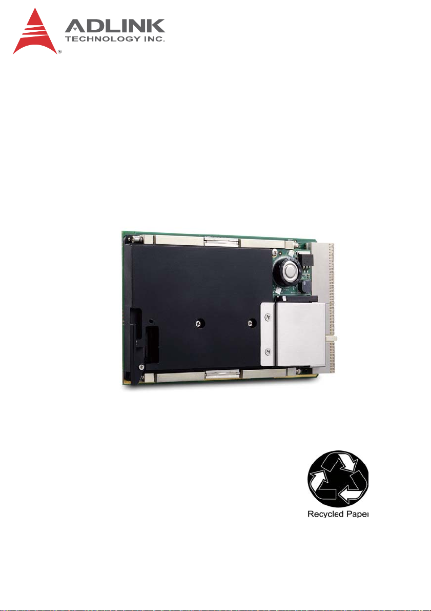
The CT-31 Series is a 3U Rugged Conduction-Cooled CompactPCI single board computer in single-slot (4HP) width form factor
featuring the ultra low voltage Intel® Atom™ N450 or D510 processor with ICH8M I/O Controller Hub. The CT-31 provides single
channel DDR2-667/800 soldered onboard memory up to 2GB,
integrated graphics on the CPU and IDE CompactFlash slot.
The optional Rear Transition Module (RTM) provides 2x SATA,
2x GbE, 1x USB, 2x COM, and VGA ports. One PCI-Express x1
port, GPIO and SMBus signals are routed to the J2 connector.
Designed for stability and packaged in a rugged conduction-cooled format, the CT-31 is suitable for long life applications
situated in extreme environments. It can withstand extreme temperatures, shock, and vibration under operation, and its components have been selected from embedded technology program s to
offer long-term availability. The CT-31 Series is ideally suited for
transportation and military applications.
CT-31
1.2 Features
X 3U Rugged Conduction-Cooled CompactPCI blade in 4HP
width form factor
X Supports Dual-Core or Single-Core Intel® Atom™ processor,
up to 1.66GHz
X Graphics and memory controllers integrated in processor
X ICH8M I/O Hub
X Single channel DDR2-667/800 SDRAM soldered onboard, up
to 2GB
X 32bit/33MHz CompactPCI Interface based on PCI specifica-
tions
X VGA port to RTM
X Two PCI-Express Giga bit Ethernet ports to RTM
X One IDE CompactFlash socket
Introduction 1
Page 14
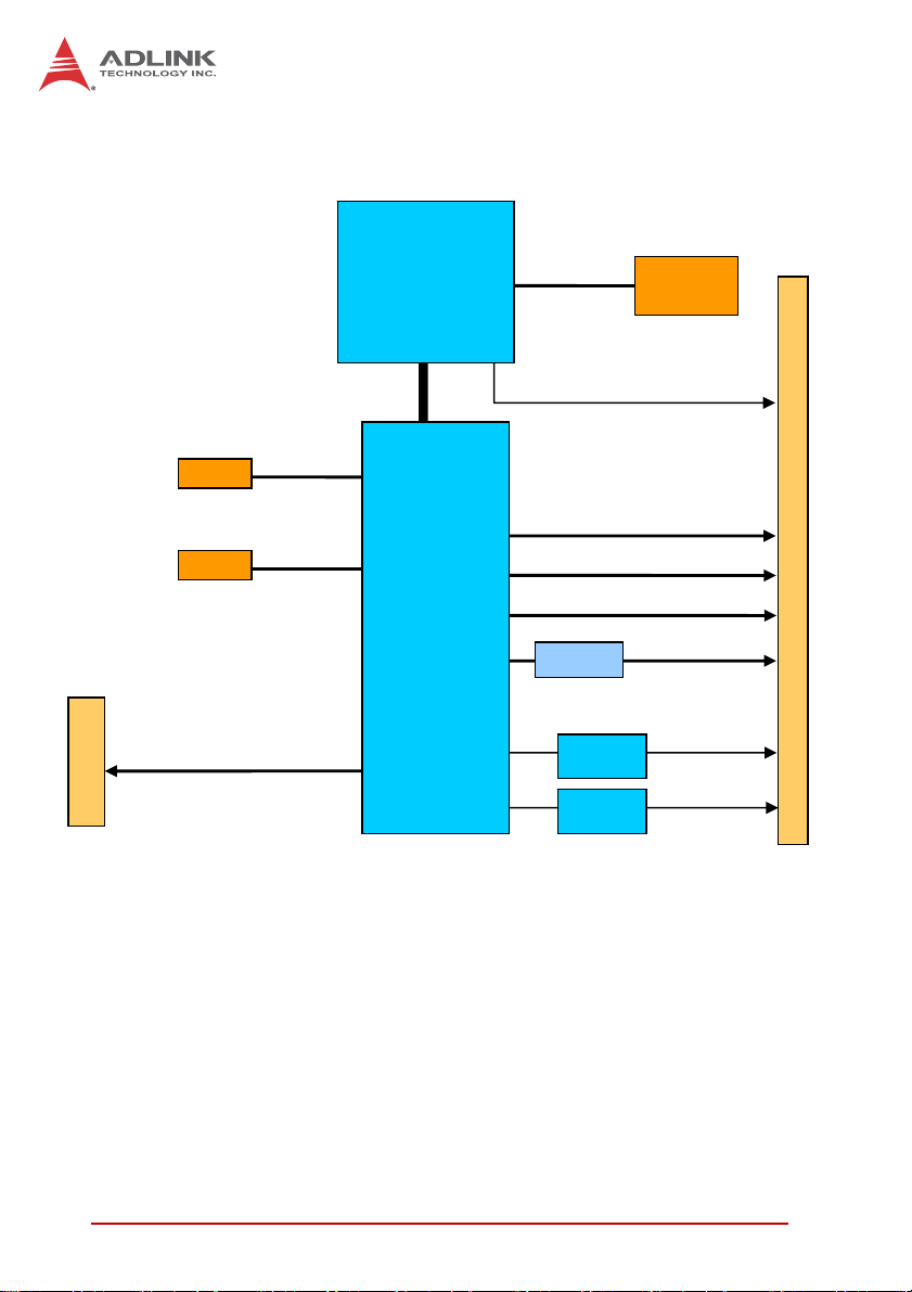
1.3 Block Diagram
Intel® Atom
Processor
N450/D510
DDR2-667/800
Soldered
Up to 2GB
J1
DMI
IDE
CF
PCIe x1, GPIO, SMBus
BIOS
PCI 32-bit/33MHz
SPI
Intel®
ICH8M
SATA 2/3
1x USB
IT8783F
Intel
82574L
Intel
82574L
Figure 1-1: CT-31 Series Functional Block Diagram
RGB
J2
COM2/3
GbE 2
GbE 1
2Introduction
Page 15

1.4 Product List
Products in the CT-31 Series include:
Processor Blade
X CT-31: 4HP width (single-slot) 3U Conduction-Cooled Com-
pactPCI blade featuring the Intel® Atom™ N450 or D510
processor, 1GB or 2GB memory soldered onboard, and
CompactFlash socket.
Rear Transition Module
X cPCI-R3610T: 8HP width, 80mm dep th Rear Transition
Module with 2x COM, USB, 2x GbE, 2x SATA, VGA
CT-31
Introduction 3
Page 16
1.5 Package Contents
The CT-31 is packaged with the following components. If any of
the items on the contents list are missing or damaged, retain the
shipping carton and packing material and contact the dealer for
inspection. Please obtain authorization before returning any product to ADLINK. The packing contents of the CT-31 Series are
non-standard configurations and may vary depending on customer
requests.
Processor Blade
X The CT-31 Series Processor Blade
Z CPU, RAM specifications will differ depending on
options selected
Z Thermal module is assembled on the board
X ADLINK All-in-One CD
X User’s manual
Rear Transition Module
X cPCI-R3610T: 8HP width, 80mm depth Rear Transition
Module with 2x COM, USB, 2x GbE, 2x SATA, VGA
The contents of non-standard CT-31 configurations may vary
depending on the customer’s requirements.
NOTE:
NOTE:
This product must be protected from static discharge and physical shock. Never remove any of the components except at a
CAUTION:
4Introduction
static-free workstation. Use the anti-static bag shipped with the
product when putting the board on a surface. Wear an
anti-static wrist strap properly grounded on one of the system's
ESD ground jacks when installing or servicing system components.
Page 17

2 Specifications
2.1 CT-31 Specifications
CT-31
CompactPCI®
Standards
Mechanical • Standard 3U CompactPCI®
Processor • µFC-BGA Intel® Atom™ Processor N450
Chipset • Intel® ICH8M I/O Controller Hub (ICH)
Memory
CompactPCI
Bus
Gigabit
Ethernet
Graphics • In te grated in Intel® Atom™ Processor
Serial Ports • Two 16C550 compatible serial ports from Super I/O IT8783
BIOS • AMIBIOS8® 16Mbit SPI flash memory
Onboard
Interfaces
• P ICMG® 2.0 CompactPCI® Rev. 3.0
• P ICMG® 2.1 Hot Swap Specification Rev.2.0
• B oard size: 100mm x 160mm
• Single-slot (4HP, 20.32mm)
• CompactPCI® connectors with J1, J2
1.66GHz, 512KB L2 cache, TDP 5.5W
• µFC-BGA dual-core Intel® Atom™ Processor D510
1.66GHz, 1MB L2 cache, TDP 13W
• Single channel unbuffered non-ECC memory soldered
onboard,
process technology)
• DDR2-667 for N450 processor, DDR2-800 for D510
processors
• PCI 32bit/ 33MHz; 3.3V, 5V universal V(I/O)
• Supports operation in system slot only
• Two PCI-Express x1 Intel® 82574L GbE controllers
• Two 10/100/1000BASE-T ports to J2 (RTM)
• VGA port to J2 (RTM)
• Analog monitor support up to QXGA 2048x1536 @60Hz
32-bit
to J2 (RTM)
CT-31:
• E IDE CompactFlash slot
cPCI-R3610T:
• 2x 7-pin SATA ports
• 2x 10-pin RS-232/422/485(+) box headers (connected to
Faceplate I/O)
up to 2GB capacity (dependent on memory
Specifications 5
Page 18

Faceplate I/O
CT-31:
•N/A
cPCI-R3610T:
• 2x USB 2.0 ports
• 10/100/1000BASE-T Ethernet port
• 2x DB-9 RS-232/422/485(+) serial ports
OS
Compatibility
• Mi crosoft Windows XP Professional, x64 Editio n
• Mi crosoft Windows Vista x64 Edition
• Mi crosoft Windows 7 x86 Edition
• Red Hat Enterprise Linux 5.3
• Fedora 12
• Other OS supp ort upon request
Environmental • Operating Temperature: -40°C to 85°C (at card edge)
• Storage Temperature: -40°C to 85°C
• Humidity: 90% non-condensing
• Shock: 40 G peak-to-peak, 11ms duration, 3-axes,
operating
• Vibration: 5Grms, 22-2000Hz,
3-axes
(1 hr. per axis), with
CompactFlash card, operating
• Conformal Coating: Yes
EMI • CE EN55022
• FCC Cla ss A
Specifications are subject to change without prior notice.
NOTE:
NOTE:
6 Specifications
Page 19

CT-31
2.2 Power Requirements
In order to guarantee stable operation of the system, it is recommended that significantly more power be provided than required.
An industrial power supply unit should be able to provide at
least twice as much power as the entire system requires of
each voltage. An ATX power supply unit should be able to provide
at least three times as much power as the entire system requires
of each voltage.
The tolerance of the voltage lines described in the CompactPCI
specification (PICMG 2.0 R3.0) is +5%/-3% for 5, 3. 3 V and ±5%
for ±12V. This specification is for power delivered to each slot and
it includes both the power supply and the backplane tolerance.
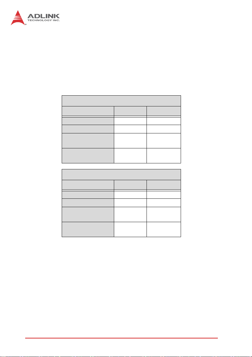
Voltage
5V +5.0 VDC +5% / -3% 50 mV
3.3V +3.3 VDC +5% / -3% 50 mV
+12V +12 VDC +5% / -5% 240 mV
-12V -12 VDC +5% / -5% 240 mV
V I/O (PCI I/O
Buffer Voltage)
GND
Nominal
Value
+3.3 VDC or
+5 VDC
Tolerance
+5% / -3% 50 mV
Max. Ripple
(P - P)
Specifications 7
Page 20
Power Consumption
This section provides information on the power consumption of
CT-31 Series when using Intel® Atom™ processors with 1GB soldered DDR2 memory and onboard 80GB SATA hard drive. The
CT-31 is powered by 5V only. Power consumption at 100% CPU
usage was measured using K-Power.
Intel® Atom™ Processor N450
OS/Mode Current 5V Total Power
DOS/Idle mode 2.83A 14.15W
Linux/Idle mode 2.38A 11.90W
Windows XP/
Idle mode
Windows® XP,
100% CPU Usage
Intel® Atom™ Processor D510
OS/Mode Current 5V Total Power
DOS/Idle mode 3.00A 15.00W
Linux/Idle mode 3.26A 16.30W
Windows XP/
Idle mode
Windows® XP,
100% CPU Usage
2.49A 12.45W
3.04A 15.20W
3.21A 16.05W
3.87A 19.35W
8 Specifications
Page 21

3 Functional Description
The following sections describe the CT-31 Series features and
functions.
3.1 Processor
CT-31
The CT-31 Series supports the
Intel® Atom™ Processor N400 and
D500 Series processors built on 45-nm Hi-K process technology.
The processor is designed for a two-chip platform as opposed to
the traditional three-chip platforms (processor, GMCH, and ICH).
The two-chip platform consists of a processor and the chipset and
enables higher performance, lower cost, easier validation, and
improved x-y footprint.
Features Atom™ N450 Atom™ D510
Clock 1.66GHz 1.66GHz
L2 cache 512KB 1MB
No. of Core(s) 1 2
Max. Power (TDP1)
T
junction, MAX
1. The high est expected sustainable power while running known
power intensive applications. TDP is not the maximum power
that the processor can dissipate.
2. The maximum supported operating temperature.
2
5.5W 13W
100°C 100°C
Intel® Atom™ Processor N450
Included in this family of processors is an integrated memory controller, integrated graphics processing unit and integrated I/O
(such as DMI) on a single silicon die.
The following list outlines the key features of this processor:
X One die, primary 32-kB instructions cache and 24-kB
write-back data cache
X Intel® Hyper-Threading Technology (2 threa ds)
X On die 512-kB, 8-way L2 cache
X Support IA 32-bit and Intel® 64 architecture
X Intel® SSE2 and SSE3 and SSSE3 support
Functional Description 9
Page 22

X Micro-FCBGA8 packaging technologies
X Thermal management support via Intel® Thermal Monitor 1
(TM1) and Intel® Thermal Monitor 2 (TM2)
X Enhanced Intel® SpeedStep Technology (EIST)
X Support L2 dynamic cache sizing
The following list outlines the key features of system memory support:
X One channel DDR2 memory
X Memory DDR2 data transfer rates of 667 MT/s
X Non-ECC, unbuffered DDR2
X 512Mb. 1-Gb,and 2-Gb DDR2 DRAM technologies supported
X Maximum of 2-GB memory capacity supported
X Maximum 1-GB memory capacity on one SO-DIMM or
Memory Down
The following list outlines the key graphics features:
X The integrated graphics controller contains a refresh of the
3rd generation graphics core
X Intel® Dynamic Video Memory Technology 4.0
X Directx* 9 compliant Pixel Shader v2.0
X 200-MHz render clock frequency
X Analog RGB display output up to resolution up to
1400x1050 @ 60Hz
10 Functional Description
Page 23

CT-31
Intel® Atom™ Processor D510
The following list provides some of the key features of this processor:
X One die, primary 32-kB instructions cache and 24-kB
write-back data cache
X Intel® Hyper-Threading Technology (2 threads per core)
X On die 2 x512-kB, 8-way L2 cache for D510 dual-core pro-
cessor
X Support IA 32-bit and Intel® 64 architecture
X Intel® SSE2 and SSE3 and SSSE3 support
X Micro-FCBGA8 packaging technologies
X Thermal management support via Intel® Thermal Monitor 1
(TM1)
The following list outlines the key features of system memory support:
X One channel DDR2 memory
X Memory DDR2 data transfer rates of 667 and 800 MT/s
X Non-ECC, unbuffered DDR2
X I/O Voltage of 1.8V for DDR2
X 512Mb. 1-Gb,and 2-Gb DDR2 DRAM technologies supported
The following list outlines the key graphics features:
X The integrated graphics controller contains a refresh of the
3rd generation graphics core
X Intel® Dynamic Video Memory Technology 4.0
X Directx* 9 compliant Pixel Shader v2.0
X 400-MHz render clock frequency
X Analog RGB display output up to resolution up to
2048x1536 @ 60Hz
Functional Description 11
Page 24

3.2 Chipset
Intel® ICH8 Mobile I/O Controller Hub
The ICH8M provides extensive I/O support. Functions and capabilities include:
X Provides 6 PCI Expressx1 ports, supporting the PCI
Express Base Specification, Revision 1.1. Each Root Port
supports 2.5GB/s bandwidth in each direction. The CT-31
utilizes two PCI Express x1 ports for two Gigabit Ethernet
controllers; routes two PCI Express x1 ports to the
board-to-board connector and one PCI Express x1 port to
the J2 connector for expansion capability.
X Enhanced DMA controller, interrupt controller, and timer functions
X Integrated Serial A TA host controller with independent DMA
operation on three ports
X Integrated IDE controller supports Ultra ATA100/66/33
X System Management Bus (SMBus) Specification, Version
2.0 with additional support for I2C devices
X Supports Intel® Matrix Storage Technology
X PCI Local Bus Specification, Revision 2.3 support for
33MHz PCI operations
3.3 Super I/O
The ITE IT8783F Super I/O is on a Low Pin Count interface supporting PS/2 keyboard/mouse; three 16C550-compatible serial
ports; hardware monitor function to monitor CPU voltage, CPU
temperature, power supply voltages and system temperature; and
Watchdog Timer with time resolution from minimum 1 second or
minute to maximum 65635 seconds or minutes on the CT-31.
3.4 Battery
The CT-31 is provided with a 5.5V Gold Capacitor for the Real
Time Clock (RTC). The Gold Capacitor is mounted on the
DB-3610CF daughter board.
12 Functional Description
Page 25
4 Board Interfaces
This chapter illustrates the board layout, connector pin
assignments, and jumper settings to familiarize users with the
CT-31 Series.
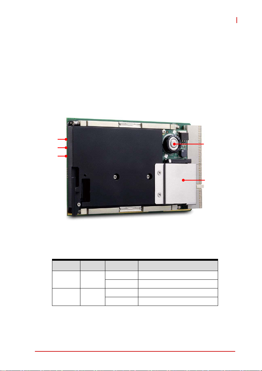
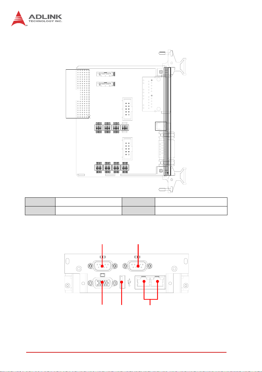
4.1 CT-31 Blade Layout
CT-31 Assembly Lay out
CT-31
WDT LED
Reset Button
Power LED
Figure 4-1: CT-31 Assembly Layout
System LEDs
LED Color Condition Indication
Power Green
WDT Red
Table 4-1: CT-31 System LED Descriptions
OFF System is off
ON System is on
OFF No Watchdog event
Blinking Watchdog event alert
Gold Capacitor
CF socket with
retention bracket
Board Interfaces 13
Page 26

CT-31 PCB Layout
DB-3610CF
CN2
SW1
CN2 DB-3610CF connector
SW1 VGA/GPIO Mode Switch
(SW3 on solder side)
J1/J2 CompactPCI connectors
Figure 4-2: CT-31 PCB Layout
J2
J1
To access SW1, see “Removing the DB-3610CF Adapter
Board” on page 21.
14 Board Interfaces
Page 27

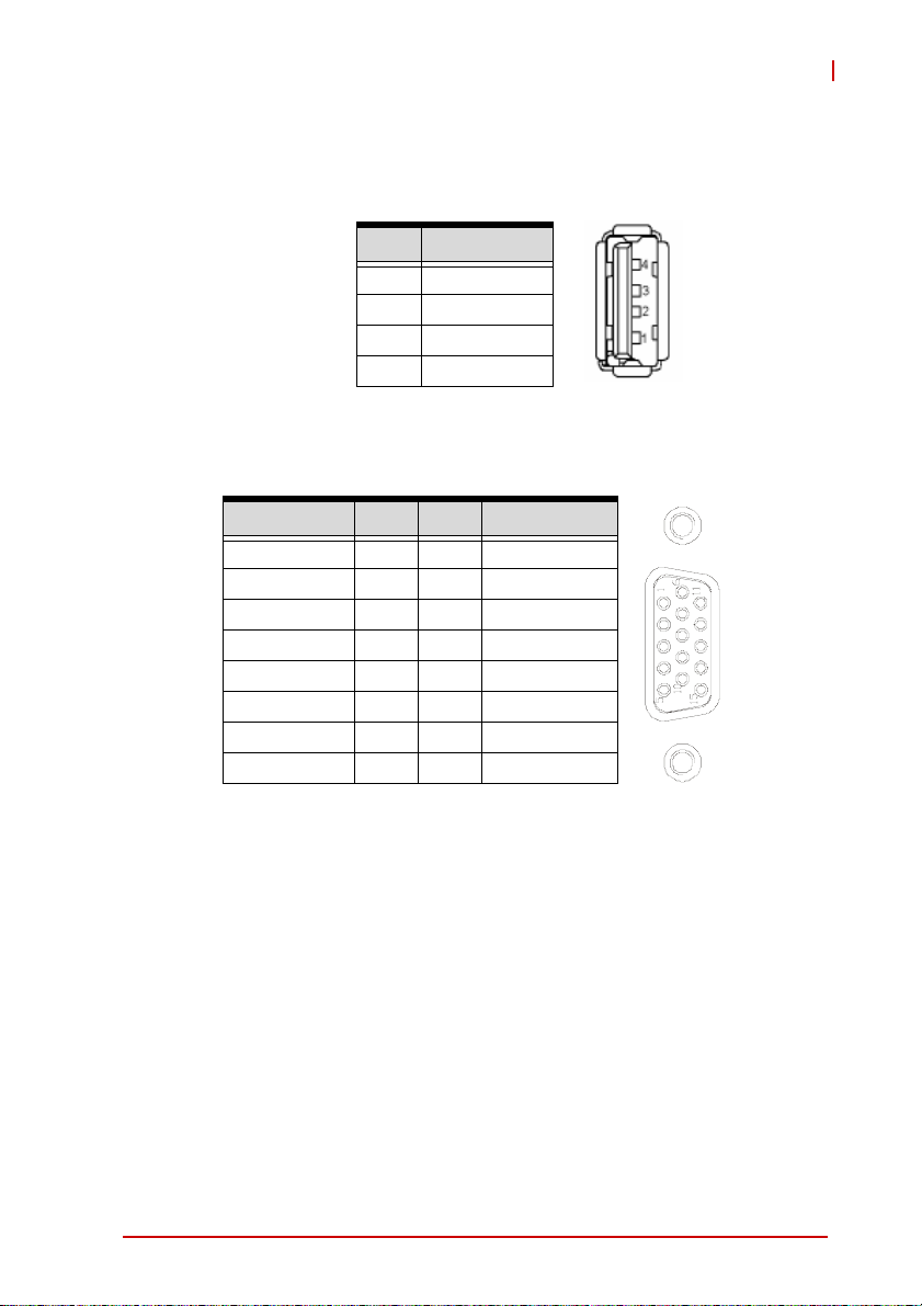
4.2 CT-31 Connector Pin Assignments
CompactFlash Connector on DB-3610CF
Signal Name Pin# Pin# Signal Name
GND 1 26 GND
DD3 2 27 DD11
DD4 3 28 DD12
DD5 4 29 DD13
DD6 5 30 DD14
DD7 6 31 DD15
CS1J 7 32 CS3J
GND 8 33 GND
GND 9 34 SDIORJ
GND 10 35 SDIOWJ
GND 11 36 5V
GND 12 37 IRQ15
5V 13 38 5V
GND 14 39 PCSEL
GND 15 40 NC
GND 16 41 BRSTDRVJ
GND 17 42 SDIORDY
DA2 18 43 NC
DA1 19 44 SDACKJ
DA0 20 45 IDEACTJ
DD0 21 46 DIAG
DD1 22 47 DD8
DD2 23 48 DD9
IOIS16J 24 49 DD10
GND 25 50 GND
CT-31
126
top
of card
2550
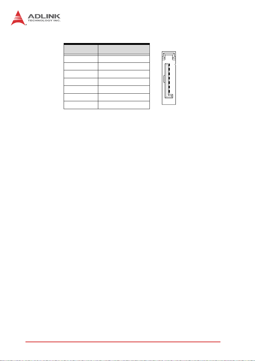
Ta ble 4-2: CompactFlash Connecto r Pin Definition
Board Interfaces 15
Page 28

DB-3610CF Connector (CN2)
Signal Name Pin # Pin # Signal Name
IDE_D7 1 2 IDE_D8
IDE_D6 3 4 IDE_D9
IDE_D5 5 6 IDE_D10
IDE_D4 7 8 IDE_D11
IDE_D3 9 10 IDE_D12
IDE_D2 11 12 IDE_D13
IDE_D1 13 14 IDE_D14
IDE_D0 15 16 IDE_D15
GND 17 18 GND
IDE_REQ-L 19 20 IDE_66DECT
IDE_IOW-L 21 22 IDE_RST-L
IDE_IOR-L 23 24 SPKR
IDE_IORDY 25 26 SIO_SPKR
IDE_ACK-L 27 28 GND
IDE_IRQ 29 30 VCC_RTC
IDE_A1 31 32 GND
IDE_A0 33 34 USB4-P
IDE_A2 35 36 USB4-N
IDE_CS1-L 37 38 P5V
IDE_CS3-L 39 40 P5V
40 39
2
1
T able 4-3: DB-3610CF Connector Pin Definition
16 Board Interfaces
Page 29

CT-31
CompactPCI J1 Connector
Pin Z A B C D E F
25 GND +5V REQ64# ENUM# +3.3V +5V GND
24 GND CPCI_AD1 +5V CPCI_VIO CPCI_AD0 ACK64# GND
23 GND P3V3 CPCI_AD4 CPCI_AD3 P5V CPCI_AD2 GND
22 GND CPCI_AD7 GND P3V3 CPCI_AD6 CPCI_AD5 GND
21 GND P3V3 CPCI_AD9 CPCI_AD8 CPCI_M66EN CPCI_CBE-L0 GND
20 GND CPCI_AD12 GND VIO CPCI_AD11 CPCI_AD10 GND
19 GND P3V3 CPCI_AD15 CPCI_AD14 GND CPCI_AD13 GND
18 GND CPCI_SERR-L GND P3V3 CPCI_PAR CPCI_CBE-L1 GND
17 GND P3V3 NC NC GND CPCI_PERR-L GND
16 GND CPCI_DEVSEL-L CPCI_PCIXCAP VIO CPCI_STOP-L CPCI_LOCK-L GND
15 GND P3V3 CPCI_FRAME-L CPCI_IRDY-L NC CPCI_TRDY - L GND
12-14 Key
11 GND CPCI_AD18 CPCI_AD17 CPCI_AD16 GND CPCI_CBE-L2 GND
10 GND CPCI_AD21 GND P3V3 CPCI_AD20 CPCI_AD19 GND
9 GND CPCI_CBE-L3 NC CPCI_AD23 GND CPCI_AD22 GND
8 GND CPCI_AD26 GND VIO CPCI_AD25 CPCI_AD24 GND
7 GND CPCI_AD30 CPCI_AD29 CPCI_AD28 GND CPCI_AD27 GND
6 GND CPCI_REQ-L0 GND P3V3 CPCI_CLK0 CPCI_AD31 GND
5 GND NC NC CPCI_RESET-L GND CPCI_GNT-L0 GND
4 GND NC CPCI_HEALTHY-L VIO NC NC GND
3 GND CPCI_IRQA-L CPCI_IRQB-L CPCI_IRQC-L P5V CPCI_IRQD-L GND
2 GND cPCI_TCK-L P5V cPCI_TMS-L NC cPCI_TDI-L GND
1 GND P5V NC cPCI_TRST-L P12V P5V GND
Table 4-4: CompactPCI J1 Connector Pin Definition
Board Interfaces 17
Page 30

CompactPCI J2 Connector
Pin Z A B C D E F
22 GND GA4 GA3 GA2 GA1 GA0 GND
21 GND CLK6 GND LAN1_TXDP0 LAN1_TXDN0 CK_ PCIE-N GND
20 GND CLK5 GND LAN1_TXDP2 GND CK_ PCIE-P GND
19 GND GND GND LAN1_TXDN2 LAN1_TXDP1 LAN1_TXDN1 GND
18 GND PCIE_TXP2 LAN1_TXDP3 LAN1_TXDN3 GND P3V3 GND
17 GND PCIE_TXN2 GND PRSTJ REQ6# GNT6# GND
16 GND GPIO0 PCIE_ RXP2 USB6-P GND PCIE_RST# GND
15 GND RGB_BLUE PCIE_ RXN2 USB6-N REQ5# GNT5# GND
14 GND GPIO1 NC USB_5_OC# SATA_TX-N1 COM2_RI# GND
13 GND LAN2_TXDP0 GND SATA_TX-P1 COM2_DTR# COM2_CTS# GND
12 GND GPIO2 LAN2_TXDN0 USB5-P SATA_RX-N1 COM2_SOUT GND
11 GND LAN2_TXDP1 GND SATA_RX-P1 COM2_RTS# COM2_SIN GND
10 GND GPIO3 LAN2_TXDN1 USB5-N GND COM2_DSR# GND
9GND
8GND
7GND RGB_RED GND +5V COM3_CTS# COM3_SOUT GND
6GND
5GND
4GND V(I/O) SATA_RX-P2 SATA_RX-N2 SATA_TX_P2 COM3_DCD# GND
3 GND CLK4 GND GNT3# REQ4# GNT4# GND
2 GND CLK2 CLK3 SYSEN# GNT2# REQ3# GND
1 GND CLK1 GND REQ1# GNT1# REQ2# GND
VSY/
GPIO4
HSY/
GPIO5
DDC_CLK/
GPIO6
DDC_DAT/
GPIO7
GND RGB_GREEN COM2_DCD# COM3_RI# GND
LAN2_TXDP2 LAN2_TXDN2 GND COM3_DTR# GND
LAN2_TXDP3 LAN2_TXDN3 GND CON3_RTS# GND
GND SATA_TX_N2 COM3_SIN COM3_DSR# GND
Table 4-5: CompactPCI J2 Connector Pin Definition
COM port
VGA (shared w/ GPIO pin 4-7 by switch selection)
Serial ATA
USB port
PCI-Express x1
Ethernet port
18 Board Interfaces
Page 31

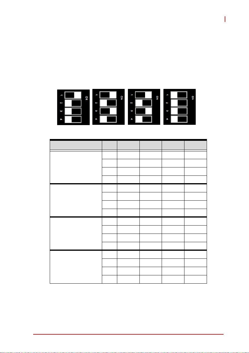
4.3 CT-31 Switch Settings
Clear CMOS Switch (SW4)
The CT-31 comes with a Clear CMOS switch to reset the
CMOS values to default. The switch is located on solder side of
the board, under the "CE" logo. Press the switch to clear the
CMOS and reset the values to default.
VGA/GPIO Mode Switches (SW1, SW3)
The VGA and GPIO 4~7 signals to J2 share the same pins and
are selected by switch settings. SW1 is located on the CT-31
component side (see “CT-31 PCB Layout” on page 14) and
SW3 is located on the solder side behind SW1 (see “Removing
the DB-3610CF Adapter Board” on page 21). When the
switches are set to VGA mode, the VGA signals are available
to J2, and there are only four GPIO signals connected to J2
(GPIO 0~3). When the switches are set to GPIO mode, there
are eight GPIO signals connected to J2 and VGA output to the
RTM is not available. The switches are set to VGA mode by
default.
CT-31
SW1 SW3
Mode SW1 SW3
VGA (default) All OFF All ON
GPIO 4~7 All ON All OFF
Table 4-6: VGA/GPIO Mode Switch Settings
To enable VGA output on the RTM, Onboard VGA Output Select
must be set to Rear in the BIOS Advanced Chipset Settings.
NOTE:
NOTE:
Board Interfaces 19
Page 32
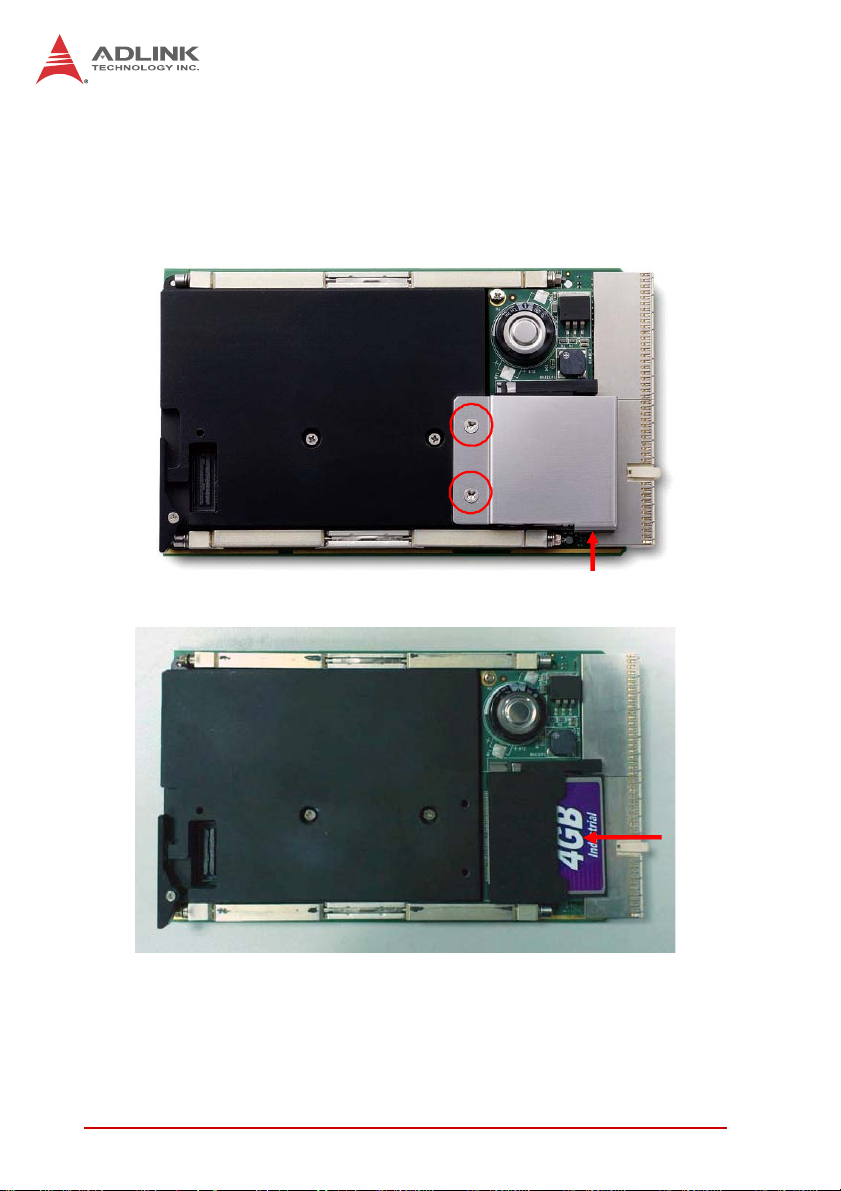
4.4 DB-3610CF Adapter Board
Installing a CF Card
1. Remove the two screws securing the CF retention
bracket. Note the flange indicated by the arrow.
2. Insert the CF card into the slot as indicated by the arrow.
3. Replace the retention bracket with securing the two
screws removed in Step 1. Make sure the bracket lies
flat on the CF card socket and the flange is under the
DB-3610 PCB.
20 Board Interfaces
Page 33
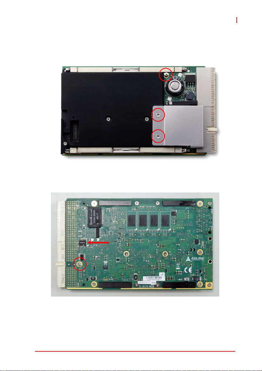
Removing the DB-3610CF Adapter Board
1. Remove the two screws securing the CF retention
bracket and the screw next to the Gold Capacitor.
2. Remove the screw indicated on the solder side of the
board. Note the location of SW3 (VGA/GPIO Mode
Switch).
CT-31
3. Lift the DB-3610CF Adapter Board from the CT-31 main
assembly.
Board Interfaces 21
Page 34
4.5 cPCI-R3610T RTM Board Layout
SATA1
SATA2
rJ2
COM2
SW1-4
COM3
SW5-8
COM2/3 COM bo x headers rJ2 CompactPCI connector
SATA1/2 SATA ports SW1-8 Switches
Figure 4-3: cPCI-R3610T RTM Board Layout
COM3
VGA
Figure 4-4: cPCI-R3610T RTM Front Panel
22 Board Interfaces
COM2
12
USB GbE x2
Page 35
CT-31
4.6 cPCI-R3610T RTM Connector Pin Assignments
USB Connector on RTM
Pin # Signal Name
1Vcc
2UV03UV0+
4GND
Table 4-7: USB Connector Pin Definition
VGA Connector on RTM (DB-15)
Signal Name Pin # Pin # Signal Name
Red 1 2 Green
Blue 3 4 N.C.
GND 5 6 GND
GND 7 8 GND
+5V. 9 10 GND
N.C. 11 12 CRTDATA
HSYNC 13 14 VSYNC
CRTCLK 15
Table 4-8: VGA Connector Pin Definition
Board Interfaces 23
Page 36
Gigabit Ethernet Connectors on RTM (RJ-45)
Pin #
1 TX+ BI_DA+
2 TX- BI_DA3 RX+ BI_DB+
4— BI_DC+
5 — BI_DC6 RX- BI_DB7— BI_DD+
8 — BI_DD-
Ta ble 4-9: GbE Connector Pin Definitions
Status
Network link is not established
or system powered off
10 Mbps
100 Mbps
1000 Mbps
10BASE-T/
100BASE-TX
Link OFF ON
Active OFF Blinking
Link Green ON
Active Green Blinking
Link Amber ON
Active Amber Blinking
1000BASE-T
81
Speed LED
(Green/Amber)
OFF OFF
Activity LED
(Yellow)
Table 4-10: Ethernet Status LED Definitions
24 Board Interfaces
Page 37
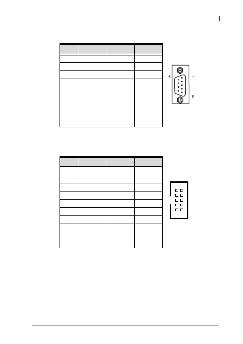
Serial Port DB-9 Connector on RTM (COM2-3)
Pin # RS-232 RS-422 RS-485(+)
1 DCD-L TXD- TXD2RXDTXD+TXD+
3TXDRXD+ —
4 DTR-L RXD- —
5 GND GND GND
6DSR-L — —
7RTS-L — —
8CTS-L — —
9RI-L — —
Table 4-11: DB-9 Serial Port Connector Pin Definition
Serial Port Box Header on RTM (COM2/3)
Pin # RS-232 RS-422 RS-485(+)
1 DCD-L TXD- TXD2DSR-L — —
3RXDTXD+TXD+
4RTS-L — —
5TXDRXD+ —
6CTS-L — —
7 DTR-L RXD- —
8RI-L — —
9 GND GND GND
10 — — —
12
910
CT-31
Table 4-12: cPCI-R3610T Serial Port Box Header Pin Definition
Board Interfaces 25
Page 38
Serial ATA Connectors on RTM
Pin # Signal
1GND
2TX+
3TX4GND
5RX6RX+
7GND
Table 4-13: Serial ATA Connector Pin Definition
1
7
26 Board Interfaces
Page 39
4.7 cPCI-R3610T RTM Switch Settings
COM2 Mode Selection Switches on RTM (SW1~SW4)
These switches on the RTM set COM2 to RS-232 full modem,
RS-422, RS-485, or RS-485+ half-duplex mode. RS-232 full
modem is set by default. See “cPCI-R3610T RTM Board Layout” on page 22 for switch locations.
CT-31
SW1
Mode Pin SW1 SW2 SW3 SW4
RS-232
RS-422
RS-485
RS-485+
Table 4-14: COM2 Mode Selection Switch Settings
SW2
1 OFF ON ON ON
2OFFOFFOFFOFF
3 OFF ON ON OFF
4OFFOFFOFFOFF
1ONOFFOFFOFF
2 OFF ON ON ON
3ONOFFOFFOFF
4 OFF ON ON OFF
1ONOFFOFFOFF
2 OFF ON ON OFF
3ONOFFOFFON
4 OFF ON ON OFF
1OFFOFFOFFOFF
2ON ON ONOFF
3 OFF OFF OFF ON
4ON ON ONOFF
SW3 SW4
Board Interfaces 27
Page 40
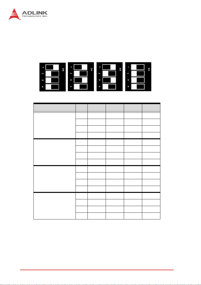
COM3 Mode Selection Switches on RTM (SW5~SW8)
These switches on the RTM set COM3 to RS-232 full modem,
RS-422, RS-485, or RS-485+ half-duplex mode. RS-232 full
modem is set by default. See “cPCI-R3610T RTM Board Layout” on page 22 for switch locations.
SW5 SW6 SW7 SW8
Mode Pin SW5 SW6 SW7 SW8
1 OFF ON ON ON
RS-232
RS-422
RS-485
RS-485+
Table 4-15: COM3 Mode Selection Switch Settings
2 OFF OFF OFF OFF
3 OFF ON ON OFF
4 OFF OFF OFF OFF
1ONOFFOFFOFF
2 OFF ON ON ON
3ONOFFOFFOFF
4 OFF ON ON OFF
1ONOFFOFFOFF
2 OFF ON ON OFF
3ONOFFOFFON
4 OFF ON ON OFF
1 OFF OFF OFF OFF
2ONONONOFF
3 OFF OFF OFF ON
4ONONONOFF
28 Board Interfaces
Page 41

5 Driver Installation
The CT-31 drivers are available on the ADLINK All-In-One CD at
X:\cPCI\cPCI-3610\, or from the ADLINK website
(http://www.adlinktech.com). This section describes the driver
installation procedures for Windows® XP.
1. Install the Windows operating system before installing
any driver. Most standard I/O device drivers are installed
during Windows installation.
2. Install the chipset driver by running the program
...\Chipset\infinst911autol.exe.
3. Install the VGA driver and utilities by running the program
...\Graphics\[CPU type]\ winxp.zip\setup.exe.
4. Install the LAN driver by running the program
…\LAN\PROXP.exe.
We recommend using the drivers provided on the ADLINK
All-in-One CD or downloaded from the ADLINK website to ensure
compatibility. Contact ADLINK to get support for VxWorks BSP.
CT-31
Driver Installation 29
Page 42

This page intentionally left blank.
30 Driver Installation
Page 43

6 Utilities
6.1 Watchdog Timer
This section describes the operation of the CT-31’s watchdog
timer (WDT). The primary function of the WDT is to monitor the
CT-31's operation and to reset the system if a software application
fails to function as programmed. The following WDT functions may
be controlled using a software application:
X enabling and disabling
X reloading timeout value
The CT-31 custom WDT circuit is implemented using the internal I/
O of the ITE SuperIO IT8783 which is at 2Eh of LPC. The basic
functions of the WDT include:
X Starting the timer countdown
X Enabling or disabling WDT
X Enabling or disabling WDT countdown LED ON
X Reloading the timeout value to keep the watchdog from tim-
ing out
X Setting the range of the timeout period from 1 second or minute
to maximum 65635 seconds or minutes
X Sending a RESET signal to the system when the watchdog
times out
CT-31
Using the Watchdog in an Application
The following section describes using the WDT functions in an
application. The WDT reset function is explained in the previous
section. This can be controlled through the registers in the CT-31's
SuperIO.
An application using the reset fe ature enab les the watch dog func tion, sets the count-down period, and reloads the timeout value
periodically to keep it from resetting the system. If the timer countdown value is not reloaded, the watchdog resets the system hardware after its counter reaches zero.
For a detailed programming sample, refer to the sample code provided in the ADLINK All-In-One CD. You can find it in the following
directory: X:\cPCI\CT-31\WDT.
Utilities 31
Page 44

Sample Code
The sample program written in C shown below offers an interactive way to test the Watchdog Timer under DOS.
#include<stdio.h>
#include<dos.h>
#define IT8783_ID1 0x87
#define IT8783_ID2 0x83
static unsigned int IT8783_ioPort = 0x2e;
//Check index port
void Enter_IT8783_Config(unsigned int flag)
{
if(flag) IT8783_ioPort = 0x4e;
switch(IT8783_ioPort)
{
case 0x2E: //Address port = 0x2E, enter keys =
0x87, 0x01, 0x55, 0x55
outportb(0x2E, 0x87);
outportb(0x2E, 0x01);
outportb(0x2E, 0x55);
outportb(0x2E, 0x55);
break;
case 0x4E: //Address port = 0x4E, enter keys =
0x87, 0x01, 0x55, 0xAA
outportb(0x4E, 0x87);
outportb(0x4E, 0x01);
outportb(0x4E, 0x55);
outportb(0x4E, 0xAA);
break;
default:
break;
}
}
//Exit index port
void Exit_IT8783_Config(unsigned int flag)
{
if(flag) IT8783_ioPort = 0x4e;
32 Utilities
Page 45

CT-31
outportb(IT8783_ioPort, 0x02);
outportb(IT8783_ioPort+1, 0x02);
}
//Check chip
void Get_IT8783_ID(unsigned int &ID1, unsigned int &ID2)
{
outportb(IT8783_ioPort, 0x20);
ID1 = inportb(IT8783_ioPort+1);
outportb(IT8783_ioPort, 0x21);
ID2 = inportb(IT8783_ioPort+1);
}
//WDT and LED program
void IT8783_3_WDTRun(unsigned int count_value, unsigned
int PLEDflag) //for CT-31
{
unsigned long tempCount;
unsigned int registerValue;
outportb(IT8783_ioPort, 0x07);
outportb(IT8783_ioPort+1, 0x07);// Device 7
outportb(IT8783_ioPort, 0xf8);
outportb(IT8783_ioPort+1, 0x00);// PLED mapping to
nothing, disable PLED function
if(PLEDflag == 1)
{
outportb(IT8783_ioPort, 0x2D);
registerValue = inportb(IT8783_ioPort + 1);
registerValue |= 0x01; // set Pin109 is GPIO
function GP60
outportb(IT8783_ioPort+1, registerValue);
outportb(IT8783_ioPort, 0xC5);
registerValue = inportb(IT8783_ioPort + 1);
registerValue &= 0xfe; // set GP60 is alternate
function
Utilities 33
Page 46

outportb(IT8783_ioPort+1, registerValue);
outportb(IT8783_ioPort, 0xCD);
registerValue = inportb(IT8783_ioPort + 1);
registerValue |= 0x01; // set GP60 is output
outportb(IT8783_ioPort+1, registerValue);
outportb(IT8783_ioPort, 0xf8);
outportb(IT8783_ioPort+1, 0x30);// PLED mapping to
GP60
outportb(IT8783_ioPort, 0xf9);
registerValue = inportb(IT8783_ioPort + 1);
registerValue |= 0x02;
registerValue &= 0xfb;
outportb(IT8783_ioPort+1, registerValue);
}
outportb(IT8783_ioPort, 0x71);
registerValue = inportb(IT8783_ioPort + 1);
registerValue |= 0xD0; // set Mouse & Keyboard
interrupt Enable
outportb(IT8783_ioPort+1, registerValue);
outportb(IT8783_ioPort, 0x73);
outportb(IT8783_ioPort+1, count_value); // set WDT
count LSB
tempCount = tempCount >> 8;
outportb(IT8783_ioPort, 0x74);
outportb(IT8783_ioPort+1, count_value); // set WDT
count MSB
if(count_value >= 60)
{
outportb(IT8783_ioPort, 0x72);
registerValue = inportb(IT8783_ioPort+1);
registerValue &= 0x8f;
registerValue |= 0x10; //enable WDT output through
PowerOK!
outportb(IT8783_ioPort+1, registerValue); // set
WDT count is minute
tempCount = count_value / 60;
if((count_value%60) > 30)
34 Utilities
Page 47

tempCount++;
if(tempCount > 65535)
tempCount = 65535;
printf("WDT timeout in %d minutes.\n", tempCount);
}
else
{
outportb(IT8783_ioPort, 0x72);
registerValue = inportb(IT8783_ioPort+1);
registerValue |= 0x80;
tempCount = count_value;
if(tempCount != 0)
{
printf("WDT timeout in %d seconds.\n",
tempCount);
registerValue |= 0x40; //Enable WDT output
through KBRST
}
else
{
printf("WDT is Disabled.\n");
registerValue &= 0xbf; //Disable WDT output
through KBRST
}
CT-31
outportb(IT8783_ioPort+1, registerValue); // set
WDT count is second
}
}
Utilities 35
Page 48

This page intentionally left blank.
36 Utilities
Page 49

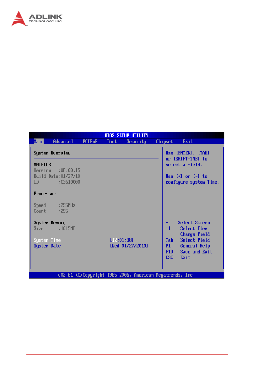
7 BIOS Setup
The following chapter describes basic navigation for the
AMIBIOS®8 BIOS setup utility.
7.1 Starting the BIOS
To enter the setup screen, follow these steps:
1. Power on the motherboard
2. Press the < Delete > key on your keyboard when you
see the following text prompt:
< Press DEL to run Setup >
3. After you press the < Delete > key, the main BIOS setup
menu displays. You can access the other setup screens
from the main BIOS setup menu , such as Chipset and
Power menus.
CT-31
Note: In most cases, the < Delete > key is used to invoke the setup
screen. There are several cases that use other keys, such as
< F1 >, < F2 >, and so on.
BIOS Setup 37
Page 50
Setup Menu
The main BIOS setup menu is the first screen that you can navigate. Each main BIOS setup menu option is described in this
user’s guide.
The Main BIOS setup menu screen has two main frames. The left
frame displays all the options that can be configured. “Grayed”
options cannot be configured, “Blue” options can be.
The right frame displays the key legend. Above the key legend is
an area reserved for a text message. When an option is selected
in the left frame, it is highlighted in white. Often a text message will
accompany it.
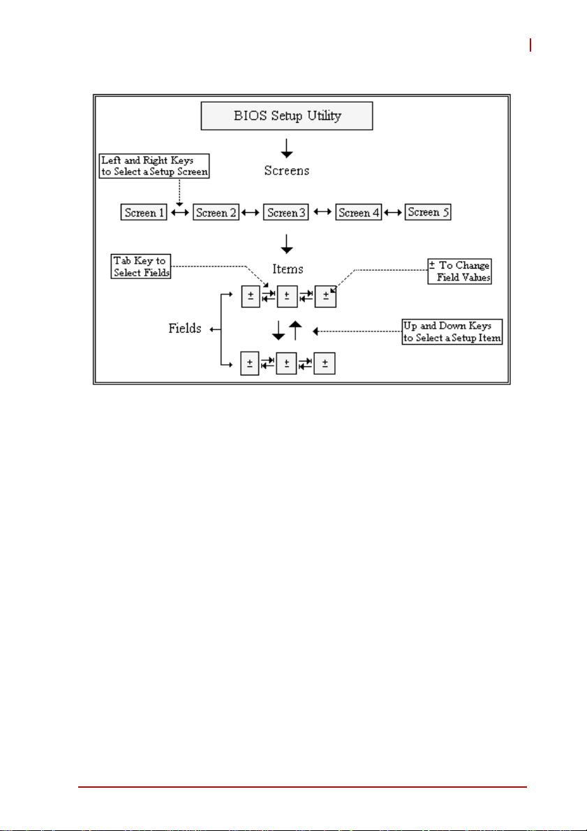
Navigation
The BIOS setup/utility uses a key-based navigation system called
hot keys. Most of the BIOS setup utility hot keys can be used at
any time during the setup navigation process.
These keys include < F1 >, < F10 >, < Enter >, < ESC >, < Arrow >
keys, and so on. .
38 BIOS Setup
Page 51
CT-31
Note: There is a hot key legend located in the r ight frame on most
setup screens.
The < F8 > key on your keyboard is the Fail-Safe key. It is not displayed on the key legend by default. To set the Fail-Safe settings
of the BIOS, press the < F8 > key on your keyboard. It is located
on the upper row of a standard 101 keyboard. The Fail-Safe settings allow the motherboard to boot up with the least amount of
options set. This can lessen the probability of conflicting settings.
Hotkey Descriptions
F1 The < F1 > key allows you to display the General Help
screen.
Press the < F1 > key to open the General Help screen.
BIOS Setup 39
Page 52
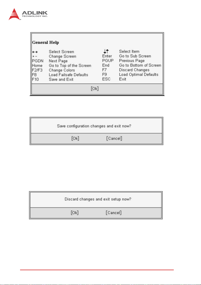
F10 The < F10 > key allows you to save any changes you have
made and exit Setup. Press the < F10 > key to save your
changes. The following screen will appear:
Press the < Enter > key to save the configuration and exit.
You can also use the < Arrow > key to select Cancel and
then press the < Enter > key to abort this functio n and return
to the previous screen.
ESC The < Esc > key allows you to discard any changes you have
made and exit the Setup. Press the < Esc > key to exit the
setup without saving your changes. The following screen will
appear:
Press the < Enter > key to discard changes and exit. You can
also use the < Arrow > key to select Cancel and then press
the < Enter > key to abort this function and return to the previous screen.
Enter The < Enter > key allows you to display or change the setup
option listed for a particular setup item. The < Enter > key
can also allow you to display the setup sub-screens.
40 BIOS Setup
Page 53

CT-31
7.2 Main Setup
When you first enter the Setup Utility , you will enter the Main setup
screen. You can always return to the Main setup screen by selecting the Main tab. There are two Main Setup options. They are
described in this section. The Main BIOS Setup screen is shown
below.
System Time/System Date
Use this option to change the system time and date. Highlight System Time or System Date using the < Arrow > keys. Enter new values using the keyboard. Press the < Tab > key or the < Arrow >
keys to move between fields. The date must be entered in MM/
DD/YY format. The time is entered in HH:MM:SS format.
Note: The time is in 24-hour format. For example, 5:30 A.M. ap-
pears as 05:30:00, and 5:30 P.M. as 17:30:00.
BIOS Setup 41
Page 54
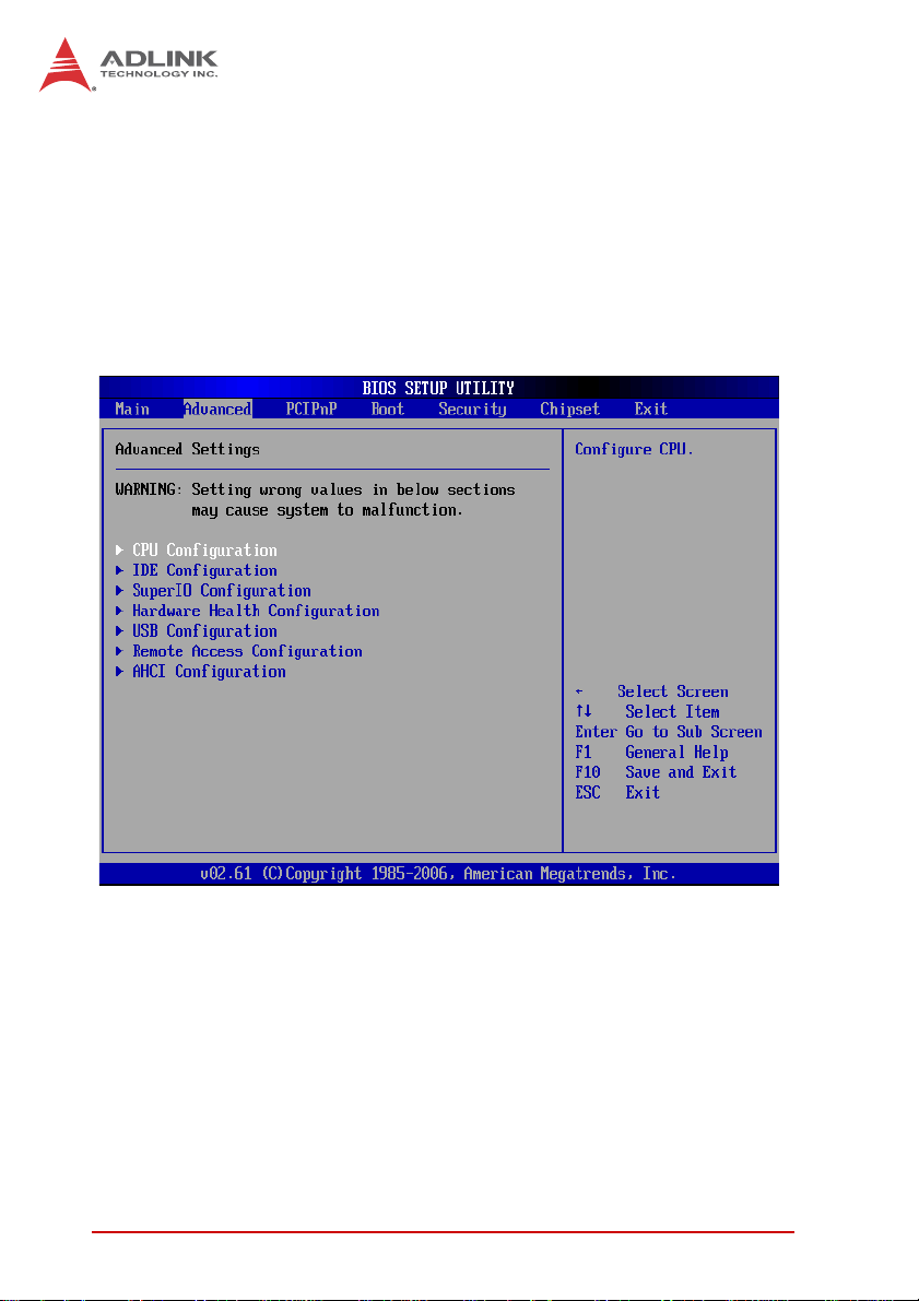
7.3 Advanced BIOS Setup
Select the Advanced tab from the setup screen to enter the
Advanced BIOS Setup screen. You can select any of the items in
the left frame of the screen to go to the sub menu for that item.
You can display an Advanced BIOS Setup option by highlighting it
using the < Arrow > keys. The Advanced BIOS Setup screen is
shown below.
The sub menus are described on the following pages.
42 BIOS Setup
Page 55
CT-31
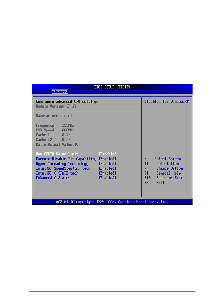
7.3.1 CPU Configuration
You can use this screen to select options for the CPU Configuration Settings. Use the up and down < Arrow > keys to select an
item. Use the < + > and < - > keys to change the value of the
selected option. A description of the selected item appears on the
right side of the screen. The settings are described on the following pages. An example of the CPU Configuration screen is shown
below.
Max CPUID Value Limit
When the computer is booted up, the operating system executes the CPUID instruction to identify the processor and its
capabilities. Before it can do so, it must first query the processor to find out the highest input value CPUID recognized. This
determines the kind of basic information CPUID can provide
the operating system. This option allows you to circumvent
problems with older operating systems.
When Enabled, the processor will limit the maximum CPUID
input value to 03h when queried, even if the processor sup-
BIOS Setup 43
Page 56

ports a higher CPUID input value. When Disabled, the processor will return the actual maximum CPUID input value of the
processor when queried.
Execute-Disable Bit Capability
Intel’s Execute Disable Bit functionality can help prevent certain classes of malicious buffer overflow attacks when combined with a supporting operating system. Exec ute Disable Bit
allows the processor to classify areas in memory where application code can execute and where it cannot. When a malicious worm attempts to insert code in the buffer, the processor
disables code execution, preventing damage and worm propagation.
Hyper-Threading Technology
This item allow you to enable or disable Hyper-Thread ing Technology.
Intel® Speedstep™ Tech
Intel® SpeedStep Technology allows the system to dynamically
adjust processor voltage and core frequency, which can result
in decreased average power consumption and decreased
average heat production.
Intel® C-State Tech
This option allows you to enable or disable Intel® C-State function.
Enhanced C-State Tech
This option allows you to enable or disable the Enhanced CState function.
44 BIOS Setup
Page 57
CT-31
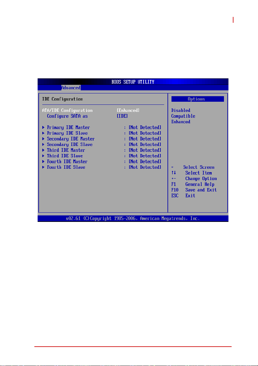
7.3.2 IDE Configuration
You can use this screen to select options for the IDE Configuration
Settings. Use the up and down < Arrow > keys to select an item.
Use the < + > and < - > keys to change the value of the selected
option.
ATA/IDE Configuration
This item specifies which mode the ATA/IDE channels should
be initialized in. The settings are Disabled, Compatible and
Enhanced.
Configure SAT A as
When running in Compatible mode, SATA channels can be
configured as a legacy IDE channel.
IDE Master/Slave
Select one of the hard disk drives to configure it. Press
< Enter > to access its sub menu.
BIOS Setup 45
Page 58

7.3.3 Super IO Configuration
You can use this screen to select options for the Super IO settings.
Use the up and down < Arrow > keys to select an item. Use the <
+ > and < - > keys to change the value of the selected option. The
settings are described on the following pages. The screen is
shown below.
Serial Port1/2 Address
Select an address for Serial Port1/2.
Port1 Options: 3F8, 3E8, 2E8, Disabled.
Port2 Options: 2F8, 3E8, 2E8, Disabled.
Serial Port1/2 IRQ
Select an IRQ for Serial Port1/2.
Options: 3, 4, 10, 11.
Serial Port3
Enable or disable Serial Port3 (address/IRQ: 3E8/10).
46 BIOS Setup
Page 59

CT-31
7.3.4 Hardware Health Configuration
This option displays the current status of all of the monitored hardware devices/components such as voltages and temperatures.
The options are Enabled and Disabled.
BIOS Setup 47
Page 60

7.3.5 USB Configuration
You can use this screen to select options for the USB Configuration. Use the up and down < Arrow > keys to select an item. Use
the < + > and < - > keys to change the value of the selected
option. The settings are described on the following pages. The
screen is shown below.
Legacy USB Support
Legacy USB Support refers to USB mouse and keyboard support. Normally if this option is not enabled, any attached USB
mouse or USB keyboard will not become available until a USB
compatible operating system is fully booted with all USB drivers loaded. When this option is enabled, any attached USB
mouse or USB keyboard can control the system even when
there are no USB drivers loaded on the system. Set this value
to enable or disable the Legacy USB Support.
X Disabled: Set this value to prevent the use of any USB
device in DOS or during system boot.
X Enabled: Set this value to allow the use of USB devices
during boot and while using DOS.
48 BIOS Setup
Page 61

CT-31
X Auto: This option auto detects USB Keyboards or M ice and
if found, allows them to be utilized during boot and while
using DOS.
USB 2.0 Controller Mode
The USB 2.0 Controller Mode c onfigures the data rate of the
USB port. The options are FullSpeed (12 Mbps) and HiSpeed
(480 Mbps).
USB Functions
Set the value to allow the system to disable, enabled and
select a set number of onboard USB ports.
USB 2.0 Controller
Enable or disable USB 2.0 functionality to all USB ports.
USB Mass Storage Device Configuration
This is a submenu for configuring the USB Mass Stor age Class
Devices when BIOS finds they are in use on USB ports. Emulation Type can be set according to the type of attached USB
mass storage device(s). If set to Auto, USB devices less than
530MB will be emulated as Floppy and those greater than
530MB will remain as hard drive. The Forced FDD option can
be used to force a hard disk type drive (such as a Zip drive) to
boot as FDD.
BIOS Setup 49
Page 62

7.3.6 AHCI Configuration
You can use this screen to select options for the AHCI Settings.
Use the up and down < Arrow > keys to select an item. Use the <
+ > and < - > keys to change the value of the selected option.
SATA Port0/1/2
Select the type of device connected to the system.
S.M.A.R.T
S.M.A.R.T. (Self-Monitoring Analysis and Reporting Technology) is a utility that monitors your disk status to predict hard
disk failure.
50 BIOS Setup
Page 63

CT-31
7.3.7 Remote Access Configuration
Remote access configuration provides the settings to allow remote
access by another computer to get POST messages and send
commands through serial port access.
Remote Access
Select this option to Enable or Disable the BIOS remote access
feature.
Enabling Remote Access requires a dedicated serial port connection. When the assigned serial port is disabled, Remote
NOTE:
NOTE:
Access should also be disabled to prevent the system from
booting abnormally.
Serial Port Number
Select the serial port you want to use for the remote access
interface. Options: COM1, COM2, COM3.
If you have changed the resource assignment of the serial
ports in Advanced> SuperIO Configuration, you must Save
NOTE:
NOTE:
BIOS Setup 51
Changes and Exit, reboot the system, and enter the setup
menu again in order to see those changes reflected in the
available Remote Access options.
Page 64

Serial Port Mode
Select the baud rate you want th e ser ia l po rt to use for console
redirection. The options are 115200 8,n,1; 57600 8,n,1; 19200
8,n,1; and 09600 8,n,1.
Flow Control
Set this option to select Flow Control for console redirection.
The settings for this value are None, Hardware, or Software.
Redirection After BIOS POST
This option allows you to set Redirection configuration after
BIOS POST. The settings for this value are Disabled, Boot
Loader, or Always.
X Disabled: Set this value to turn off the redirection after POST
X Boot Loader: Set this value to allow the redirection to be
active during POST and Boot Loader.
X Always: Set this value to allow the redirection to be always
active.
Terminal Type
This option is used to select either VT100/VT-UTF8 or ANSI
terminal type. The settings for this value are ANSI, VT100, or
VT-UTF8.
VT-UTF8 Combo Key Support
This option enables VT-UTF8 Combination Key Support for
ANSI/VT100 terminals. The settings for this value are Enabled
or Disabled.
Sredir Memory Display Delay
This option gives the delay i n se co nd s to di sp l ay m emo ry in f ormation. The options for this value are No Delay, D e l a y 1 S ec ,
Delay 2 Sec, or Delay 4 Sec.
52 BIOS Setup
Page 65
CT-31
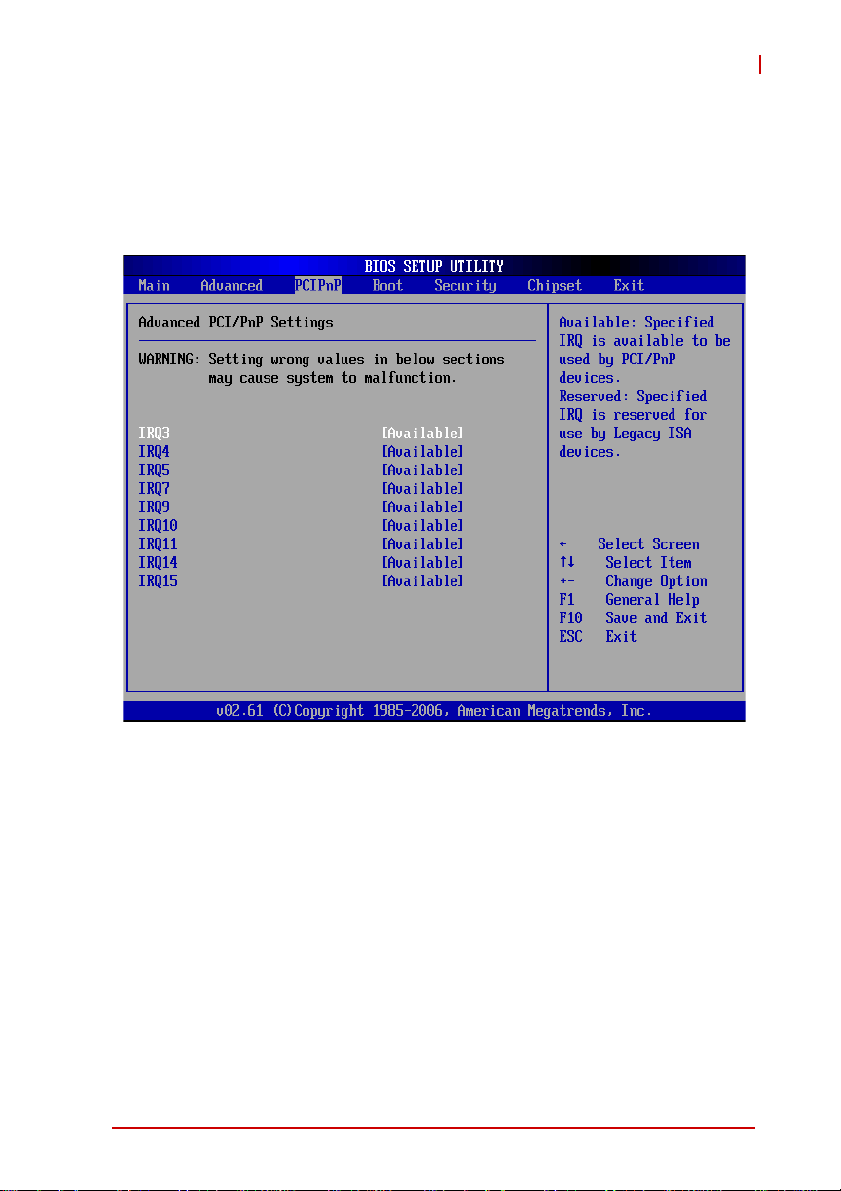
7.4 Advanced PCI/PnP Settings
Select the PCI/PnP tab from the setup screen to enter the Plug
and Play BIOS Setup screen. You can display a Plug and Play
BIOS Setup option by highlighting it using the < Arrow > keys. The
Plug and Play BIOS Setup screen is shown below.
IRQ Channel
Set this value to allow the IRQ channel settings to be modified.
X Available: This setting allows the specified IRQ/DMA chan-
nel to be used by a PCI/PnP device.
X Reserved: This setting allows the specified IRQ/DMA chan-
nel to be used by a legacy ISA device.
BIOS Setup 53
Page 66
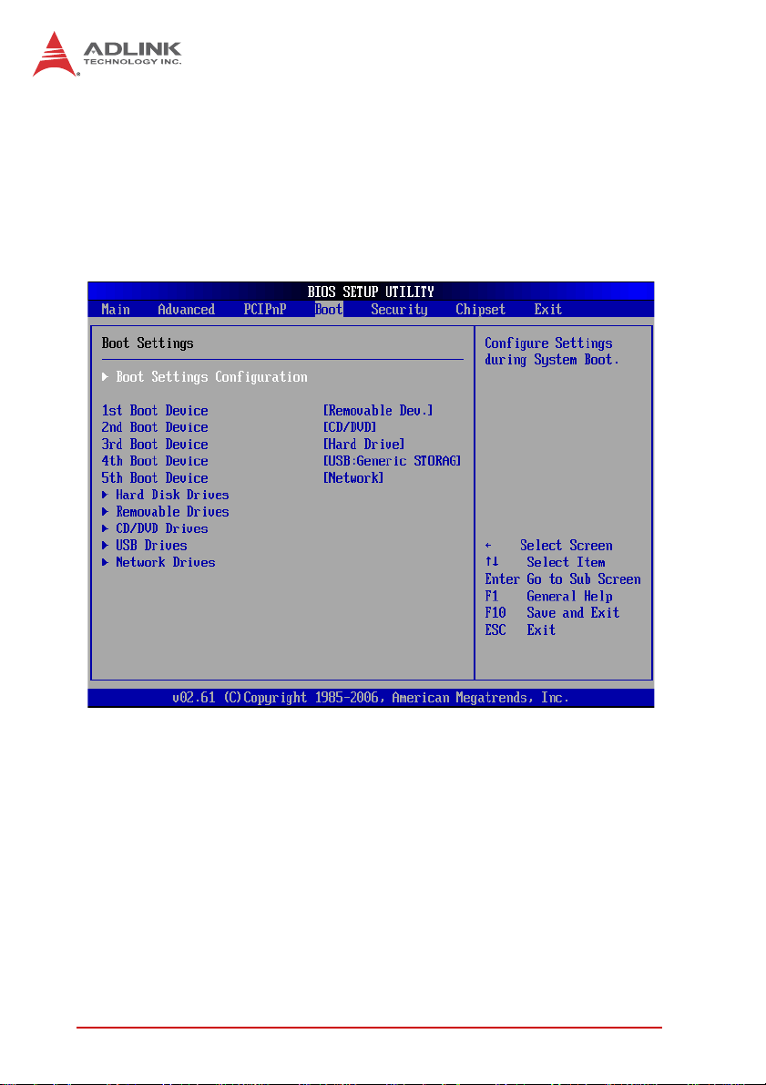
7.5 Boot Settings
Select the Boot tab from the setup screen to enter the Boot BIOS
Setup screen. You can select any of the items in the left frame of
the screen, such as Boot Device Priority, to go to the sub menu for
that item. You can display a Boot BIOS Setup option by highlighting it using the < Arrow > keys. The Boot Settings screen is sh own
below:
54 BIOS Setup
Page 67
CT-31
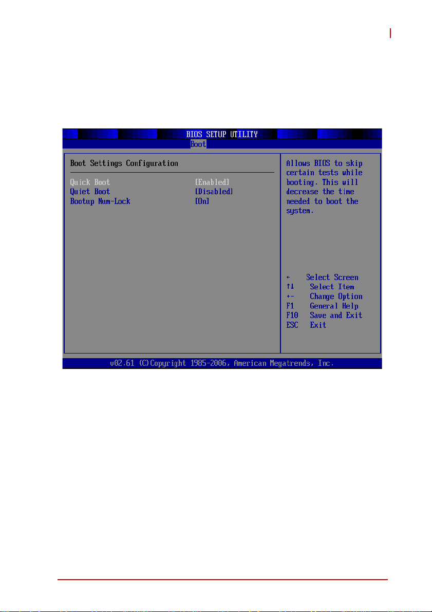
7.5.1 Boot Settings Configuration
Use this screen to select options for the Boot Settings Configuration. Use the up and down <Arrow> keys to sel ect an it em. Use t he
<Plus> and <Minus> keys to change the value of the selected
option.
Quick Boot
Enabling this setting will cause the BIOS power-on self test
routine to skip some of its tests during bootup for faster system
boot.
Quiet Boot
When this feature is enabled, the BIOS will display the OEM
logo during the boot-up sequence, hiding normal POST messages. When it is disabled, the BIOS will display the normal
POST messages, instead of the OEM logo.
Bootup Num-Lock
Allows you to select the power-on state for Num-Lock.
BIOS Setup 55
Page 68
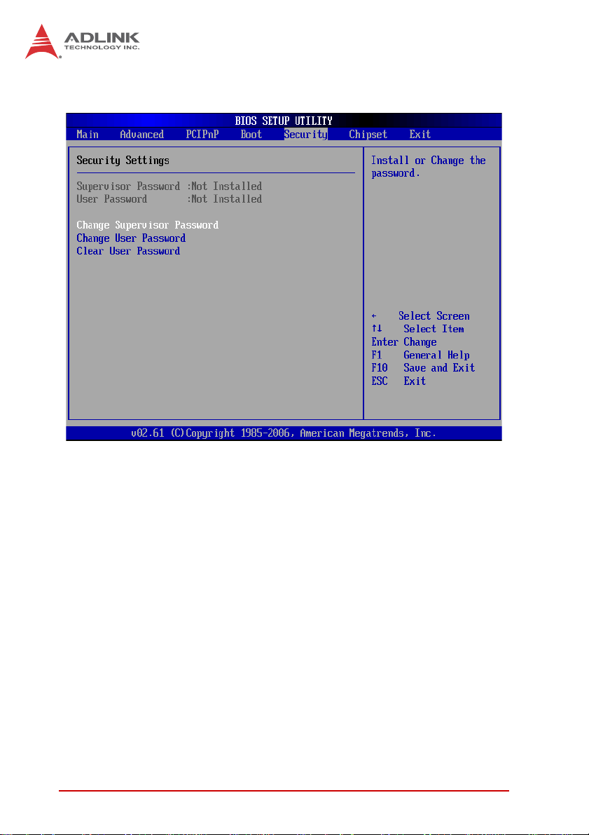
7.6 Security Setup
Password Support
Two Levels of Password Protection
Provides both a Supervisor and a User password. If you use
both passwords, the Supervisor password must be set first.
The system can be configured so that all users must enter a
password every time the system boots or when Setup is executed, using either or either the Supervisor password or User
password.
The Supervisor and User passwords activate two different levels of password security. If you select password support, you
are prompted for a one to six character password. Type the
password on the keyboard. The password does not appear on
the screen when typed. Make sure you write it down. If you forget it, you must drain NVRAM and re-configure.
56 BIOS Setup
Page 69

CT-31
Remember the Password
Keep a record of the new password when the password is
changed. If you forget the password, you must erase the system configuration information in NVRAM.
To access the sub menu for the following ite m s, s ele ct th e item
and press < Enter >:
X Change Supervisor Password
X Change User Password
X Clear User Password
Supervisor Password
Indicates whether a supervisor password has been set.
User Password
Indicates whether a user password has been s et .
Change Supervisor Password
Select this option and press < Enter > to access the sub menu.
You can use the sub menu to change the supervisor password.
Change User Password
Select this option and press < Enter > to access the sub menu.
You can use the sub menu to change the user password.
Clear User Password
Select this option and press < Enter > to access the sub menu.
You can use the sub menu to clear the user password.
Change Supervisor Password
Select Change Supervisor Password from the Security Setup
menu and press < Enter >.
Enter New Password:
Type the password and press < Enter >. The screen does not display the characters entered. Retype the password as prompted
BIOS Setup 57
Page 70

and press < Enter >. If the password confirmation is incorrect, an
error message appears. The password is stored in NVRAM after
completes.
Change User Password
Select Change User Password from the Security Setup menu and
press < Enter >.
Enter New Password:
Type the password and press < Enter >. The screen does not dis play the characters entered. Retype the password as prompted
and press < Enter >. If the password confirmation is incorrect, an
error message appears. The password is stored in NVRAM after
completes.
58 BIOS Setup
Page 71
CT-31
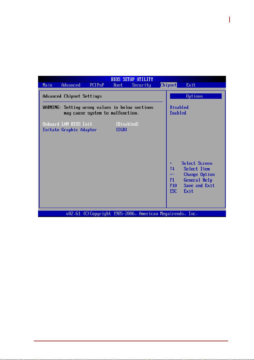
7.7 Chipset Setup
Select the Chipset tab from the setup screen to enter the Chipset
BIOS Setup screen. You can select any of the items in the left
frame of the screen to go to the sub m enu for t hat it em. T he C hipset BIOS Setup screen is shown below.
Onboard LAN BIOS Init
Set this value to enable/disable the invoking of onboard LAN’s
PXE ROM. Disabling can shorten the POST time by not initializing
LAN PXE ROM. Enable it if boot from LAN is needed.
Initial Graphics Adapter
Select which graphics controller to use as the primary boot device.
BIOS Setup 59
Page 72
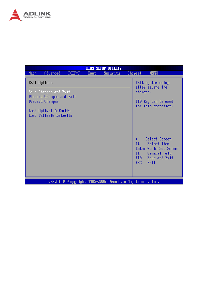
7.8 Exit Menu
Select the Exit tab from the setup screen to enter the Exit BIOS
Setup screen. You can display an Exit BIOS Setup option by highlighting it using the < Arrow > keys. The Exit BIOS Setup screen is
shown below.
Save Changes and Exit
When you have completed the system configuration changes,
select this option to leave Setup and reboot the computer so the
new system configuration parameters can take effect.
Save Configuration Changes and Exit Now?
[Ok] [Cancel]
appears in the window. Select Ok to save changes and exit.
Discard Changes and Exit
Select this option to quit Setup without making any permanent
changes to the system configuration.
60 BIOS Setup
Page 73

CT-31
Discard Changes and Exit Setup Now?
[Ok] [Cancel]
appears in the window. Select Ok to discard changes and exit.
Discard Changes
Select Discard Changes from the Exit menu and press < Enter >.
Select Ok to discard changes.
Load Optimal Defaults
Automatically sets all Setup options to a complete set of default
settings when you select this option. The Optimal settings are
designed for maximum system performance, but may not work
best for all computer applications. In particular, do not use the
Optimal Setup options if your computer is experiencing system
configuration problems.
Select Load Optimal Defaults from the Exit menu and press
< Enter >.
Select Ok to load optimal defaults.
Load Failsafe Defaults
Automatically sets all Setup options to a complete set of default
settings when you select this option. The Failsafe settings are
designed for maximum system stability, but not maximum performance. Select the FailSafe Setup options if your computer is
experiencing system configuration problems.
Select Load Fail-Safe Defaults from the Exit menu and press
< Enter >.
Load FailSafe Defaults?
[Ok] [Cancel]
appears in the window. Select Ok to load FailSafe defaults.
BIOS Setup 61
Page 74

This page intentionally left blank.
62 BIOS Setup
Page 75

CT-31
Important Safety Instructions
For user safety, please read and follow all instructions,
WARNINGS, CAUTIONS, and NOTES marked in this manual
and on the associated equipment before handling/operating the
equipment.
X Read these safety instructions carefully.
X Keep this user’s manual for future reference.
X Read the specifications section of this manual for detailed
information on the operating environment of this equipment.
X When installing/mounting or uninstalling/removing
equipment:
Z Turn off power and u nplug any power cords/cables.
X To avoid electrical shock and/or damage to equipment:
Z Keep equipment away from water or liquid sources;
Z Keep equipment away from high heat or high humidity;
Z Keep equipment properly ventilated (do not block or
cover ventilation openings);
Z Make sure to use recommended voltage and powe r
source settings;
Z Always install and operate equipment near an easily
accessible electrical socket-outlet;
Z Secure the power cord (do not place any obje ct on /ove r
the power cord);
Z Only install/attach and operate equipment on stable
surfaces and/or recommended mountings; and,
Z If the equipment will not be used for long periods of time,
turn off and unplug the equipment from its power source.
Important Safety Instructions 63
Page 76

X Never attempt to fix the equipment. Equipmen t sho u ld on ly
be serviced by qualified personnel.
A Lithium-type battery may be provided for uninterrupted, backup
or emergency power.
Risk of explosion if battery is replaced with one of an incorrect
WARNING:
type. Dispose of used batteries appropriately.
X Equipment must be serviced by authorized technicians
when:
Z The power cord or plug is damaged;
Z Liquid has penetrated the equipment;
Z It has been exposed to high humidity/moisture;
Z It is not functioning or does not function according to the
user’s manual;
Z It has been dropped and/or damaged; and/or,
Z It has an obvious sign of breakage.
64 Important Safety Instructions
Page 77

Getting Service
Contact us should you require any service or assistance.
ADLINK Technology, Inc.
Address: 9F, No.166 Jian Yi Road, Zhonghe District
New Taipei City 235, Taiwan
ᄅקؑխࡉ৬ԫሁ 166 ᇆ 9 ᑔ
Tel: +886-2-8226-5877
Fax: +886-2-8226-5717
Email: service@adlinktech.com
Ampro ADLINK Technology, Inc.
Address: 5215 Hellyer Avenue, #110, San Jose, CA 95138, USA
Tel: +1-408-360-0200
Toll Free: +1-800-966-5200 (USA only)
Fax: +1-408-360-0222
Email: info@adlinktech.com
ADLINK Technology (China) Co., Ltd.
Address: Ϟ⍋Ꮦ⌺ϰᮄᓴ∳催⾥ᡔು㢇䏃 300 ো(201203)
300 Fang Chun Rd., Zhangjiang Hi-Tech Park,
Tel: +86-21-5132-8988
Fax: +86-21-5132-3588
Email: market@adlinktech.com
ADLINK Technology Beijing
Address: ࣫ҀᏖ⍋⎔Ϟഄϰ䏃 1 োⲜ߯ࡼ E ᑻ 801 ᅸ(100085)
Tel: +86-10-5885-8666
Fax: +86-10-5885-8625
Email: market@adlinktech.com
ADLINK Technology Shenzhen
Address: ⏅ഇᏖቅ⾥ᡔು催ᮄϗ䘧᭄ᄫᡔᴃು
Tel: +86-755-2643-4858
Fax: +86-755-2664-6353
Email: market@adlinktech.com
Pudong New Area, Shanghai, 201203 China
Rm. 801, Power Creative E, No. 1, B/D
Shang Di East Rd., Beijing, 100085 China
A1 2 ὐ C (518057)
2F, C Block, Bldg. A1, Cyber-Tech Zone, Gao Xin Ave. Sec. 7,
High-Tech Industrial Park S., Shenzhen, 518054 China
CT-31
Getting Service 65
Page 78

ADLINK Technology (Europe) GmbH
Address: Nord Carree 3, 40477 Duesseldorf, Germany
Tel: +49-211-495-5552
Fax: +49-211-495-5557
Email: emea@adlinktech.com
ADLINK Technology, Inc. (French Liaison Office)
Address: 15 rue Emile Baudot, 91300 Massy CEDEX, France
Tel: +33 (0) 1 60 12 35 66
Fax: +33 (0) 1 60 12 35 66
Email: france@adlinktech.com
ADLINK Technology Japan Corporation
Address: ͱ101-0045 ᵅҀ䛑ҷ⬄⼲⬄䤯ފ⬎ 3-7-4
⼲⬄ 374 ɛɳ 4F
KANDA374 Bldg. 4F, 3-7-4 Kanda Kajicho,
Chiyoda-ku, Tokyo 101-0045, Japan
Tel: +81-3-4455-3722
Fax: +81-3-5209-6013
Email: japan@adlinktech.com
ADLINK Technology, Inc. (Korean Liaison Office)
Address: 昢殾柢 昢爎割 昢爎壟 1675-12 微汾瘶捒娯 8猻
8F Mointer B/D,1675-12, Seocho-Dong, Seocho-Gu,
Seoul 137-070, Korea
Tel: +82-2-2057-0565
Fax: +82-2-2057-0563
Email: korea@adlinktech.com
ADLINK Technology Singapore Pte. Ltd.
Address: 84 Genting Lane #07-02A, Cityneon Design Centre,
Singapore 349584
Tel: +65-6844-2261
Fax: +65-6844-2263
Email: singapore@adlinktech.com
ADLINK Technology Singapore Pte. Ltd. (Indian Liaison Office)
Address: No. 1357, "Anupama", Sri Aurobindo Marg, 9th Cross,
JP Nagar Phase I, Bangalore - 560078, India
Tel: +91-80-65605817
Fax: +91-80-22443548
Email: india@adlinktech.com
66 Getting Service
 Loading...