

ADLINK cPCI-7200 User Manual

NuDAQ / NuIPC
PCI-7200 / cPCI-7200 / LPCI-7200S
12MB/S High Speed Digital I/ O Card
User’s Manual
Manual Rev. 2.00
Revision Date: March 31, 2006
Part No: 50-11102-1030
Advance Technologies; Automate the World.

Copyright 2006 ADLINK TECHNOLOGY INC.
All Rights Reserved.
The information in this document is subject to change without prior
notice in order to improve reliability, design, and function and does
not represent a commitment on the part of the manufacturer.
In no event will the manufacturer be liable for direct, indirect, special, incidental, or consequential damages arising out of the use or
inability to use the product or documentation, even if advised of
the possibility of such damages.
This document contains proprietary information protected by copyright. All rights are reserved. No part of this manual may be reproduced by any mechanical, electronic, or other means in any form
without prior written permission of the manufacturer.
Trademarks
NuDAQ, NuIPC, DAQBench are registered trademarks of ADLINK
TECHNOLOGY INC.
Product names mentioned herein are used for identification purposes only and may be trademarks and/or registered trademarks
of their respective companies.
Getting Service from ADLINK
Customer Satisfaction is top priority for ADLINK Technology Inc.
Please contact us should you require any service or assistance.
ADLINK TECHNOLOGY INC.
Web Site: http://www.adlinktech.com
Sales & Service: Service@adlinktech.com
TEL: +886-2-82265877
FAX: +886-2-82265717
Address: 9F, No. 166, Jian Yi Road, Chungho City,
Taipei, 235 Taiwan
Please email or FAX this completed service form for prompt and
satisfactory service.
Company Information
Company/Organization
Contact Person
E-mail Address
Address
Country
TEL FAX:
Web Site
Product Information
Product Model
OS:
Environment
M/B: CPU:
Chipset: BIOS:
Please give a detailed description of the problem(s):


Table of Contents
Table of Contents..................................................................... i
List of Tables.......................................................................... vi
List of Figures ....................................................................... vii
1 Introduction ........................................................................ 1
1.1 Applications ......................................................................... 1
1.2 Features............................................................................... 2
1.3 Specifications....................................................................... 3
1.4 Supporting Software ............................................................ 5
Programming Library ...................................................... 5
DAQ-LVIEW PnP: LabVIEW® Driver ............................. 6
PCIS-VEE: HP-VEE Driver ............................................. 6
PCIS-OCX: ActiveX Controls .......................................... 6
DASYLabTM PRO .......................................................... 6
PCIS-DDE: DDE Server and InTouchTM ...................... 6
PCIS-ISG: ISaGRAFTM driver ....................................... 7
PCIS-ICL: InControlTM Driver ........................................ 7
PCIS-OPC: OPC Server ................................................. 7
2 Installation .......................................................................... 9
2.1 Contents .............................................................................. 9
2.2 Unpacking.......................................................................... 10
2.3 Device Installation for Windows Systems .......................... 10
2.4 PCI-7200/cPCI-7200/LPCI-7200S Layout ......................... 11
2.5 Hardware Installation Outline............................................. 15
2.6 Connector Pin Assignments .............................................. 16
PCI-7200 Pin Assignments ........................................... 16
cPCI-7200 Pin Assignments ......................................... 18
LPCI-7200S Pin Assignments ...................................... 19
2.7 8254 for Timer Pacer Generation ...................................... 21
2.8 LPCI-7200S PCI Bus Signaling ......................................... 22
2.9 Onboard Pull-ups and Terminations in digital input ........... 22
3 Register Format................................................................ 25
3.1 I/O Registers Format ......................................................... 25
3.2 Digital Input Register (BASE + 10) .................................... 25
Table of Contents i

3.3 Digital Output Register (BASE + 14).................................. 26
3.4 DIO Status & Control Register (BASE + 18)...................... 26
3.5 Interrupt Status & Control Register (BASE + 1C) .............. 29
3.6 8254 Timer Registers (BASE + 0) ..................................... 32
4 Operation Theory .............................................................. 33
4.1 Direct Program Control ...................................................... 33
4.2 Timer Pacer Mode ............................................................. 34
4.3 External Clock Mode.......................................................... 35
4.4 Handshaking ...................................................................... 36
4.5 Timing Characteristic ......................................................... 38
5 C/C++ Libraries ................................................................. 41
5.1 Libraries Installation ........................................................... 42
5.2 Programming Guide........................................................... 43
Naming Convention ...................................................... 43
Data Types ................................................................... 43
5.3 _7200_Initial ...................................................................... 44
@ Description ............................................................... 44
@ Syntax ...................................................................... 44
@ Argument .................................................................. 44
@ Return Code ............................................................. 44
5.4 _7200_Switch_Card_No .................................................... 46
@ Description ............................................................... 46
@ Syntax ...................................................................... 46
@ Argument .................................................................. 46
@ Return Code ............................................................. 46
5.5 _7200_AUX_DI .................................................................. 47
@ Description ............................................................... 47
@ Syntax ...................................................................... 47
@ Argument .................................................................. 47
@ Return Code ............................................................. 47
5.6 _7200_AUX_DI_Channel................................................... 48
@ Description ............................................................... 48
@ Syntax ...................................................................... 48
@ Argument .................................................................. 48
@ Return Code ............................................................. 48
5.7 _7200_AUX_DO ................................................................ 49
@ Description ............................................................... 49
@ Syntax ...................................................................... 49
ii Table of Contents

@ Argument ................................................................. 49
@ Return Code ............................................................. 49
5.8 _7200_AUX_DO_Channel................................................. 50
@ Description ............................................................... 50
@ Syntax ...................................................................... 50
@ Argument ................................................................. 50
@ Return Code ............................................................. 50
5.9 _7200_DI ........................................................................... 51
@ Description ............................................................... 51
@ Syntax ...................................................................... 51
@ Argument ................................................................. 51
@ Return Code ............................................................. 51
5.10 _7200_DI_Channel............................................................ 52
@ Description ............................................................... 52
@ Syntax ...................................................................... 52
@ Argument ................................................................. 52
@ Return Code ............................................................. 52
5.11 _7200_DO ......................................................................... 53
@ Description ............................................................... 53
@ Syntax ...................................................................... 53
@ Argument ................................................................. 53
@ Return Code ............................................................. 53
5.12 _7200_DO_Channel .......................................................... 54
@ Description ............................................................... 54
@ Syntax ...................................................................... 54
@ Argument ................................................................. 54
@ Return Code ............................................................. 54
5.13 _7200_Alloc_DMA_Mem ................................................... 55
@ Description ............................................................... 55
@ Syntax ...................................................................... 55
@ Argument ................................................................. 55
@ Return Code ............................................................. 56
5.14 _7200_Free_DMA_Mem ................................................... 57
@ Description ............................................................... 57
@ Syntax ...................................................................... 57
@ Argument ................................................................. 57
@ Return Code ............................................................. 57
5.15 _7200_Alloc_DBDMA_Mem .............................................. 58
@ Description ............................................................... 58
@ Syntax ...................................................................... 58
Table of Contents iii

@ Argument .................................................................. 58
@ Return Code ............................................................. 58
5.16 _7200_Free_DBDMA_Mem............................................... 59
@ Description ............................................................... 59
@ Syntax ...................................................................... 59
@ Argument .................................................................. 59
@ Return Code ............................................................. 59
5.17 _7200_DI_DMA_Start........................................................ 60
@ Description ............................................................... 60
@ Syntax ...................................................................... 61
@ Argument .................................................................. 62
@ Return Code ............................................................. 63
5.18 _7200_DI_DMA_Status ..................................................... 64
@ Description ............................................................... 64
@ Syntax ...................................................................... 64
@ Argument .................................................................. 64
@ Return Code ............................................................. 64
5.19 _7200_DI_DMA_Stop ........................................................ 65
@ Description ............................................................... 65
@ Syntax ...................................................................... 65
@ Argument .................................................................. 65
@ Return Code ............................................................. 65
5.20 _7200_DblBufferMode ....................................................... 66
@ Description ............................................................... 66
@ Syntax ...................................................................... 66
@ Argument .................................................................. 66
@ Return Code ............................................................. 66
5.21 _7200_CheckHalfReady .................................................... 67
@ Description ............................................................... 67
@ Syntax ...................................................................... 67
@ Argument .................................................................. 67
@ Return Code ............................................................. 67
5.22 _7200_DblBufferTransfer................................................... 68
@ Description ............................................................... 68
@ Syntax ...................................................................... 68
@ Argument .................................................................. 68
@ Return Code ............................................................. 68
5.23 _7200_GetOverrunStatus .................................................. 69
@ Description ............................................................... 69
@ Syntax ...................................................................... 69
iv Table of Contents

@ Argument ................................................................. 69
@ Return Code ............................................................. 69
5.24 _7200_DO_DMA_Start...................................................... 70
@ Description ............................................................... 70
@ Syntax ...................................................................... 70
@ Argument ................................................................. 70
@ Return Code ............................................................. 71
5.25 _7200_DO_DMA_Status ................................................... 72
@ Description ............................................................... 72
@ Syntax ...................................................................... 72
@ Argument ................................................................. 72
@ Return Code ............................................................. 72
5.26 _7200_DO_DMA_Stop ...................................................... 73
@ Description ............................................................... 73
@ Syntax ...................................................................... 73
@ Argument ................................................................. 73
@ Return Code ............................................................. 73
5.27 _7200_DI_Timer ................................................................ 74
@ Description ............................................................... 74
@ Syntax ...................................................................... 74
@ Argument ................................................................. 75
@ Return Code ............................................................. 75
5.28 _7200_DO_Timer .............................................................. 76
@ Description ............................................................... 76
@ Syntax ...................................................................... 76
@ Argument ................................................................. 77
@ Return Code ............................................................. 77
6 Double Buffer Mode Principle......................................... 79
7 Limitations ........................................................................ 81
Warranty Policy..................................................................... 83
Table of Contents v

List of Tables
Table 2-1: CN1A Pin Assignments .......................................... 19
Table 2-2: CN1B Pin Assignments .......................................... 20
Table 2-3: Pull-ups and termination of PCI/cPCI-7200 and LPCI-
7200S. .................................................................... 22
Table 5-1: Data Types ............................................................. 43
vi List of Tables

List of Figures
Figure 2-1: PCI-7200 Layout Diagram ....................................... 11
Figure 2-2: cPCI-7200 Layout Diagram ..................................... 12
Figure 2-3: LPCI-7200S Layout Diagram................................... 13
Figure 2-4: LPCI-7200S with standard PCI bracket ................... 14
Figure 2-5: CN1 Pin Assignments.............................................. 17
Figure 2-6: CN2 Pin Assignments.............................................. 17
Figure 2-7: CN Pin Assignments................................................ 18
Figure 2-8: 8254 configuration ................................................... 21
Figure 2-9: Digital input pull-up resistor and termination circuit dia-
gram. ....................................................................... 23
Figure 6-1: Double Buffer Mode................................................. 79
List of Figures vii


1 Introduction
The PCI-7200, cPCI-7200, and LPCI-7200S are PCI/CompactPCI/
Low profile PCI form factor high-speed digital I/O cards, consisting
of 32 digital input channels, and 32 digital output channels. High
performance design and state-of-the-art technology make this
card suitable for high-speed digital input and output applications.
The PCI-7200 performs high-speed data transfers using bus-mastering DMA via the 32-bit PCI bus architecture. The maximum data
transfer rates can be up to 12MB per second - very suitable for
interfacing high-speed peripherals with your computer system.
Several different digital I/O operation modes are supported:
1. Direct Program Control: the digital inputs and outputs
can be accessed and controlled by its corresponding I/O
ports directly.
2. Timer Pacer Mode: the digital input and output opera-
tions are handled by internal timer pacer clock and transferred by bus mastering DMA.
3. External Clock Mode: the digital input operations are
handled by an external input strobe signal (I_REQ) and
transferred by bus mastering DMA.
4. Handshaking: through the REQ and ACK signals, digi-
tal I/O data can utilize simple handshaking data transfer.
1.1 Applications
X Interface to high-speed peripherals
X High-speed data transfers from other computers
X Digital I/O control
X Interface to external high-speed A/D and D/A converter
X Digital pattern generator
X Waveform and pulse generation
X BCD interface driver
Introduction 1

1.2 Features
The PCI-7200 high-speed DIO Card provides the following
advanced features:
X 32 TTL digital input channels
X 32 TTL digital output channels
X Transfer up to 12M Bytes per second
X High output driving and low input loading
X 32-bit PCI bus, Plug and Play
X Onboard internal timer pacer clock
X Internal timer controls input sampling rate
X Internal timer controls digital output rate
X ACK and REQ for handshaking
X Onboard 32-byte FIFO for both digital input and output
X Extra 2k double word digital input FIFO for cPCI-7200
X Four auxiliary digital input and output channels (cPCI-7200
only)
X Diode terminators for 32 input channels and control sig-
nals(cPCI-7200/LPCI-7200S)
X Multiple interrupt sources are selectable by software
2Introduction

1.3 Specifications
Digital I/O (DIO)
X Number of DI Channels: 32 TTL compatible
X Number of DO Channels: 32 TTL compatible
X Data Transfer Mode
Z Program I/O
Z Internal timer pacer transfer
Z External I_REG strobe input
Z Handshake data transfer
X Maximum Transfer Speed:
Z 3MHz (12MB/sec) by external clock, handshake or
external strobe
Z 2MHz (8MB/sec) by internal timer pacer transfer
X FIFO:
Z Eight words (32-bit) (for PCI-7200/LPCI-7200S)
Z 2k + 8 words (32-bit) (for cPCI-7200 Digital input chan-
nels)
X Input Voltage:
Z Low: Min. 0V; Max. 0.8V
Z High: Min. +2.0V
X Input Load:
Z Low: +0.5V @ -0.6mA max.
Z High: +2.7V @ +20µA max.
X Output Voltage:
Z Low: Min. 0V; Max. 0.5V
Z High: Min. +2.7V
X Driving Capacity:
Z Low: Max. +0.5V at 24mA (Sink)
Z High: Min. 2.4V at -3.0mA (Source)
Introduction 3

Programmable Counter
X Device: 82C54-10, with a 4MHz time base
X Timer 0: DI clock source
X Timer 1: DO clock source
X Timer2: Base clock of Timer #0 and Timer #1
X Pacer Output: 0.00046Hz to 2MHz
General Specifications
X Operating Temperature: 0ºC to 60ºC
X Storage Temperature: -20ºC to 80ºC
X Humidity: 5 to 95%, non-condensing
X Connector:
Z PCI-7200:one 37-pin D-type and one 40-pin ribbon con-
nector
Z cPCI-7200:one 100-pin SCSI-type connector
Z LPCI-7200S: two 68-pin SCSI-type connectors
X Dimension:
Z PCI-7200:Compact size, only 148mm (L) X 102mm (H)
Z cPCI-7200:Standard 3U CompactPCI form factor
Z LPCI-7200S: Low Profile PCI, 167.64mm (L) X 64.41mm
(H)
X Power Consumption:
Z PCI-7200: +5V @ 720 mA typical
Z cPCI-7200: +5V @ 820 mA typical
Z LPCI-7200S: +5V @ 500 mA typical
X PCI signaling environment:
Z PCI-7200: 5V board supports a 5V PCI BUS
Z cPCI-7200: 3U Eurocard form factor, CompactPCI com-
pliant (PICMG 2.0 R2.1)
Z LPCI-7200S: Universal board, supports a 3.3V or 5V PCI
BUS
4Introduction

1.4 Supporting Software
ADLINK provides versatile software drivers and packages for
users’ different approach to building a system. We not only provide
programming library for many Windows systems, but also provide
drivers for many software packages including LabVIEW®, HP
TM
VEE
All software options are included in the ADLINK CD. Commercial
software drivers require licenses. Without the software license,
users can still install them and run the demo version for two hours
for demonstration purpose. Please contact an ADLINK dealer to
purchase licenses.
Programming Library
For customers writing customized programs, we provide function
libraries for many different operating systems, including:
, DASYLabTM, InTouchTM, InControlTM, ISaGRAFTM, etc.
X DOS Library: Borland C/C++ and Microsoft C++ (function
descriptions are included in this user’s guide).
X Windows 95 DLL: For VB, VC++, Delphi, BC5 (functions
descriptions are included in this user’s guide).
X PCIS-DASK: Includes device drivers and DLL for Windows
98/NT/2000/XP. The DLL is binary compatible across Windows 98/NT/2000/XP. The developing environment can be
VB, VC++, Delphi, BC5, or any Windows programming language that allows calls to a DLL. The PCIS-DASK user’s
guide and function reference manual are on the CD. Please
refer the PDF manual files under the following directory:
\Manual_PDF\Software\PCIS-DASK
X PCIS-DASK/X: Includes device drivers and a shared library
for Linux. The developing environment can be Gnu C/C++
or any programming language that allows linking to a
shared library. The PCIS-DASK/X user's guide and function
reference manual are on the CD (\Manual_PDF\Software\PCIS-DASK-X).
The above software drivers are shipped with the board. Please
refer to the “Software Installation Guide” to install these drivers.
Introduction 5

DAQ-LVIEW PnP: LabVIEW® Driver
DAQ-LVIEW PnP contains the VIs, which are used to interface
with NI’s LabVIEW® software package. The DAQ-LVIEW PnPW
supports Windows 98/NT/2000/XP. The LabVIEW® drivers are
shipped free of charge with the board. These can be installed and
used without license. For further detailed information about DAQLVIEW PnP, please refer to the user’s guide in the CD.
(\\Manual\Software Package\DAQ-LVIEW PnP)
PCIS-VEE: HP-VEE Driver
PCIS-VEE includes the user objects, which are used to interface
with the HP VEE software package. PCIS-VEE supports Windows
95/98/NT. The HP-VEE drivers are shipped free with the board.
Users can install and use them without a license. For detailed
information about PCIS-VEE, please refer to the user’s guide on
the CD.
(\Manual_PDF\Software\PCIS-VEE)
PCIS-OCX: ActiveX Controls
It is recommended that customers who are familiar with ActiveX
controls and VB/VC++ programming to use the PCIS-OCX
ActiveX Control components library for developing applications.
The PCIS-OCX is designed under Windows 98/NT/2000/XP. For
further information on PCIS-OCX, please refer to the user’s guide
in the CD.
(\\Manual\Software Package\PCIS-OCX)
DASYLabTM PRO
DASYLab is an easy-to-use software package that provides easysetup instrument functions such as FFT analysis. Please contact
ADLINK to get DASYLab PRO, which include DASYLab and
ADLINK hardware drivers.
PCIS-DDE: DDE Server and InTouchTM
DDE stands for Dynamic Data Exchange specifications. The
PCIS-DDE includes the PCI cards’ DDE server. The PCIS-DDE
6Introduction

server is included on the ADLINK CD. It requires a license. The
DDE server can be used in conjunction with any DDE client under
Windows NT.
PCIS-ISG: ISaGRAFTM driver
The ISaGRAF WorkBench is an IEC1131-3 SoftPLC control program development environment. The PCIS-ISG includes ADLINK
products’ target drivers for ISaGRAF under the Windows NT environment. The PCIS-ISG is included on the ADLINK CD. It requires
a license.
PCIS-ICL: InControlTM Driver
PCIS-ICL is the InControl driver, which support the Windows NT.
The PCIS-ICL is included on the ADLINK CD. It requires a license.
PCIS-OPC: OPC Server
PCIS-OPC is an OPC Server that can link with OPC clients. Many
software packages on the market provide OPC clients. PCIS-OPC
supports Windows NT. It requires a license.
Introduction 7

8Introduction

2 Installation
This chapter describes how to install the PCI-7200. Package contents and unpacking information are described. Because the PCI7200 is a Plug and Play device, there are no jumper or DIP switch
settings for configuration. The interrupt number and I/O port
address are assigned by the system BIOS during system boot up.
2.1 Contents
In addition to this User's Manual, the package includes the following items:
X PCI-7200 Digital I/O & Counter Card
X ACL-10437: 40-pin to 37-pin D-Sub cable
or
X cPCI-7200 Digital I/O & Counter Module for 3U
X 100-pin SCSI connector assembly
or
X LPCI-7200S Low profile Digital I/O & Cunter Card
X ADLINK CD
X Software Installation Guide
If any of these items is missing or damaged, contact the ADLINK
dealer. Save the shipping materials and carton to ship or store the
product in the future.
Installation 9

2.2 Unpacking
The PCI-7200 card contains sensitive electronic components that
can be easily damaged by static electricity.
The work area should have a grounded anti-static mat. The operator should be wearing an anti-static wristband, grounded at the
same point as the anti-static mat.
Inspect the card module carton for obvious damage. Shipping and
handling may cause damage to the module. Ensure there is no
shipping and handling damage on the module before proceeding.
After opening the card module carton, remove the system module
and place it only on a grounded anti-static surface component side
up.
Again inspect the module for damage. Press down on all the socketed IC's to ensure that they are properly seated. Do this only with
the module place on a firm flat surface.
Note: DO NOT APPLY POWER TO THE CARD IF IT HAS BEEN
DAMAGED.
You are now ready to install your PCI-7200.
2.3 Device Installation for Windows Systems
Once Windows 95/98/2000 has started, the Plug and Play function
of Windows system will find the new NuDAQ/NuIPC cards. If this
is the first time to installing NuDAQ/NuIPC cards in this system,
Windows will require device information source. Please refer to
the “Software Installation Guide” for instructions on installing the
device.
10 Installation
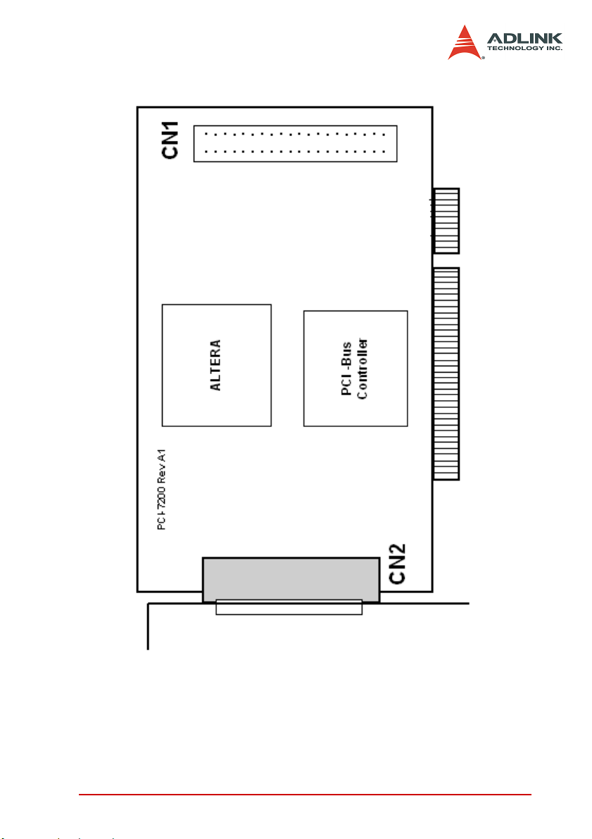
2.4 PCI-7200/cPCI-7200/LPCI-7200S Layout
Figure 2-1: PCI-7200 Layout Diagram
Installation 11
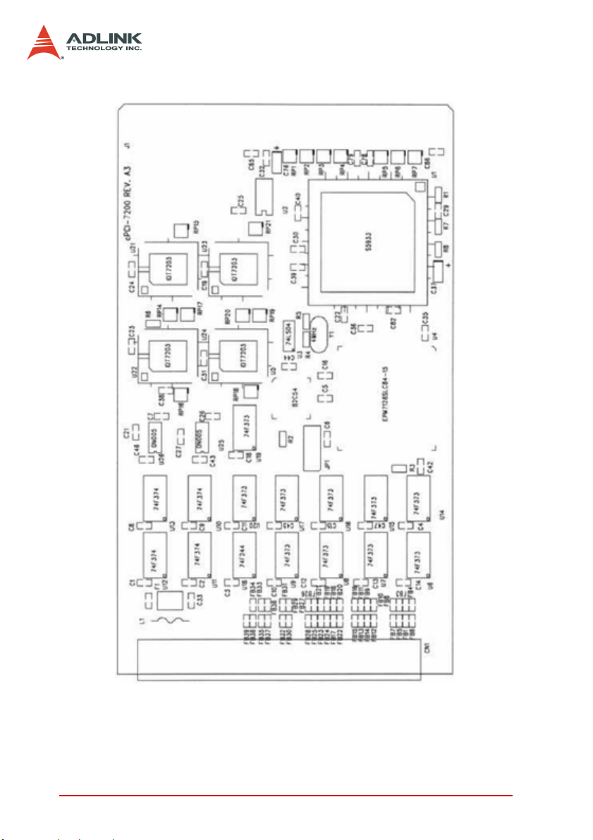
Figure 2-2: cPCI-7200 Layout Diagram
12 Installation
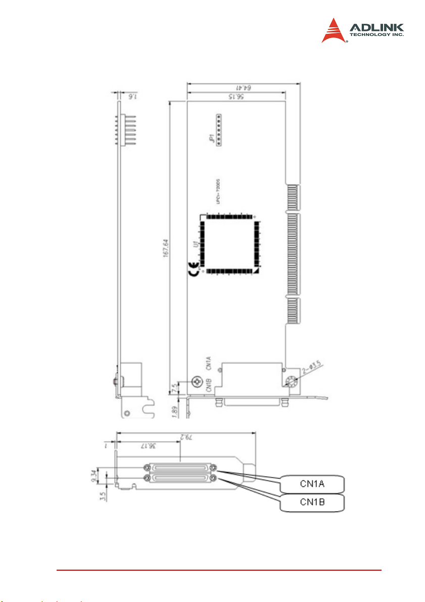
Figure 2-3: LPCI-7200S Layout Diagram
Installation 13
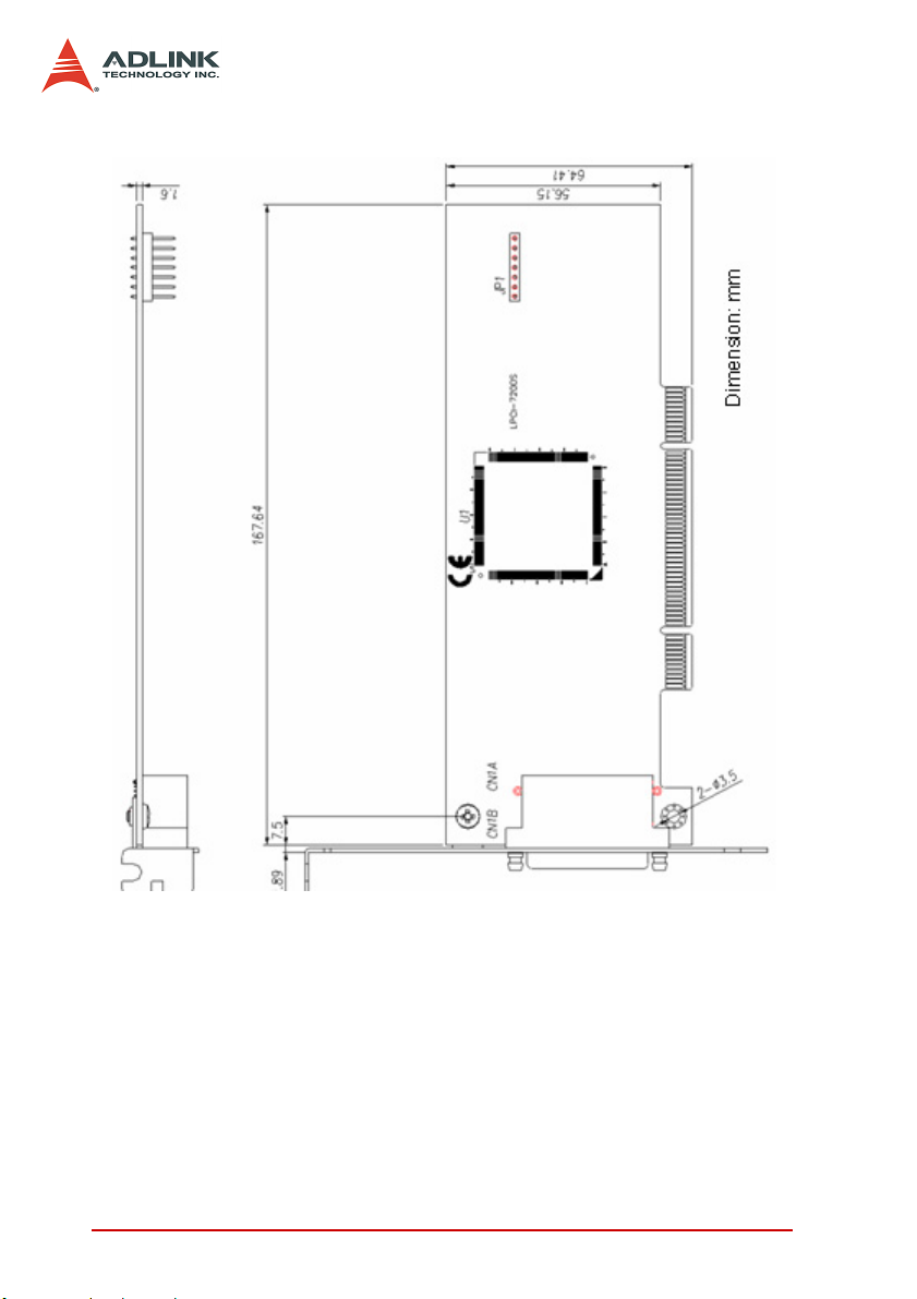
Figure 2-4: LPCI-7200S with standard PCI bracket
14 Installation

2.5 Hardware Installation Outline
Hardware configuration
These PCI cards (or CompactPCI, Low Profile PCI cards) are
equipped with a Plug and Play PCI controller that requests
base addresses and interrupts according to PCI standard. The
system BIOS will install the system resource based on the PCI
cards’ configuration registers and system parameters (which
are set by system BIOS). Interrupt assignment and memory
usage (I/O port locations) of the PCI cards can be assigned by
system BIOS only. These system resource assignments are
done on a board-by-board basis. It is not recommended to
assign the system resource by any other methods.
PCI slot selection
The PCI and Low-Profile PCI cards can be inserted to any PCI
slot without any configuration for system resource. CompactPCI peripheral slots are marked with a circle on the backplane.
Please note that the PCI, CompactPCI, and Low-Profile PCI
system board must provide bus-mastering capability to operate
this board well.
Installation Procedure
1. Turn off the computer
2. Turn off all accessories (printer, modem, monitor, etc.)
connected to the computer
3. Remove the cover from your computer
4. Select a 32-bit PCI slot. PCI slots are shorter than the
ISA or EISA slots, and are usually white or ivory in
colour.
5. Before handling the PCI cards, discharge any static
buildup on your body by touching the metal case of the
computer. Hold the edge of the card and do not touch
the components.
6. Position the board into the PCI selected slot.
7. Secure the card in place at the rear panel of the system.
Installation 15
2.6 Connector Pin Assignments
PCI-7200 Pin Assignments
The PCI-7200 comes equipped with one 37-pin D-Sub connector
(CN2) located on the rear mounting plate and one 40-pin female
flat cable header connector (CN1). The CN2 is located on the rear
mounting plate; the CN1 is on front of the board. Refer section 2.4
PCI-7200‘s layout.
CN2 is used for digital inputs (DI 0 to DI 15) and digital outputs
(DO 0 to DO 15) The reminding digital I/O channels DI 16 to DI 31
and DO 16 to DO 31 are on CN1. The pin assignment of CN1 and
CN2 is illustrated in the Figures 2-5 and 2.3.
Legend:
DO n Digital Output CH n
DI n Digital Input CH n
GND Ground
ACK ACK handshaking signal
REQ REQ handshaking signal
I_TRG Input signal to start DI data sampling
O_TRG Output signal can be controlled by software
16 Installation

O_ACK
O_ACK
O_REQ
O_REQ
DI16
DI16
DI17
DI17
DI18
DI18
DI19
DI19
DI20
DI20
DI21
DI21
DI22
DI22
DI23
DI23
DI24
DI24
DI25
DI25
DI26
DI26
DI27
DI27
DI28
DI28
DI29
DI29
DI30
DI30
DI31
DI31
+5V
+5V
1
1
1
34
34
3
56
56
56
78
78
78
910
910
910
11 12
11 12
11 12
13 14
13 14
13 14
15 16
15 16
15 16
17
17
17
19
19
19
21
21
21
23 24
23 24
23 24
25 26
25 26
25 26
27 28
27 28
27 28
29
29
29
31
31
31
35
35
35
37
37
37
39 40
39 40
39
N/C
N/C
2
2
DO16
DO16
DO17
DO17
DO18
DO18
DO19
DO19
DO20
DO20
DO21
DO21
DO22
DO22
DO23
DO23
18
18
18
DO24
DO24
20
20
20
DO25
DO25
22
22
22
DO26
DO26
DO27
DO27
DO28
DO28
DO29
DO29
30
30
30
DO30
DO30
32
32
32
DO31
DO31
3433
3433
3433
GND
GND
36
36
36
O_TR1
O_TR1
38
38
38
N/C
N/C
N/C
N/C
Figure 2-5: CN1 Pin Assignments
DI 0
DI 1
DI 2
DI 3
DI 4
DI 5
DI 6
DI 7
DI 8
DI 9
DI10
DI11
DI12
DI13
DI14
DI15
+5V
I_ACK
I_REQ
1
2
3
4
5
6
7
8
9
10
11
12
13
14
15
16
17
18
19
20
DO0
21
DO1
22
DO2
23
DO3
24
DO4
25
DO5
26
DO6
27
DO7
28
DO8
29
DO9
30
DO10
31
DO11
32
DO12
33
DO13
34
DO14
35
DO15
36
GND
37
I_TRG
Figure 2-6: CN2 Pin Assignments
Installation 17
 Loading...